|
TE Project #1
A kit of components for the Logic
Probe is available from EM Kits. |
|
|

One of the handiest pieces of test equipment is a LOGIC PROBE. It
allows you to test and see what is happening at different points in a
circuit.
There are basically two different types of circuits: DIGITAL and
ANALOGUE.
The voltages (waveforms) in an analogue circuit are rising and falling
but in most cases the amplitude will not be high enough to be detected
by our Logic Probe.
That's why it is mainly used for a digital circuit.
There are different categories of digital circuits, according
to the supply-voltage.
1. Low voltage designs: 3.3v operation,
2. TTL-Level designs: 5v operation,
3. CMOS designs: 5 - 15v operation, and
4. HIGH voltage designs, above 15v operation.
Our Logic Probe will work on circuits operating between 5v and
15v.
It is mainly designed for testing Talking Electronics digital projects
as they operate at fairly low frequencies and have 5v-9v supplies. All
our digital projects are simple and easy to put together and work the
first time they are switched on, but it is interesting to see what is
happening, when a circuit is working and it's hand when modifying a
circuit. It is interesting to see a line
going HIGH and LOW and tracing through the circuit to see how an output
is "sitting" and how it affects other parts of a circuit.
HOW THE
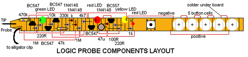
CIRCUIT WORKS
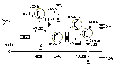
The circuit consists of 3 "building Blocks." A building block is any
group of parts that form a circuit and the circuit can be given a "name"
or a "feature." You can create your own Building Block and its an easy
way to describe the operation of a set of components in a circuit.
It simplifies a circuit and makes it "easy-to-understand." We will
describe this circuit without using any technical terminology.
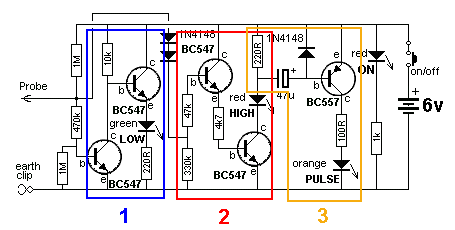
The first building block consists of a common-emitter transistor and an
emitter follower.
This is how to "see" it working:
Remove the first transistor. The second transistor "slides up and down"
on two wires, the first wire being the base wire containing the 10k and
the second wire being the collector wire and the emitter wire. As the
transistor slides up towards the 6v rail, the LED turns on brighter.
As the transistor moves towards the 0v rail the LED turns off.
Now put the first transistor back into the circuit.
As the first transistor turns on, it pulls the second transistor towards
the 0v rail and the LED turns off.
When the first transistor turns off, the 10k pulls the second transistor
towards the 6v rail. This is how the two transistors work.
In front of the first building block are three resistors that form a
voltage divider.
They are selected so that the voltage on the base of the first
transistor is just above 0.7v so the transistor is turned on and pulls
the second towards the 0v rail and the green LED is not illuminated.
Don't worry about trying to work out the actual voltage on the probe as
the voltage divider is a very complex arrangement in this design.
Next we have building Block 2.
This building block consists of two transistors in a "super Alpha"
arrangement or "Super Transistor." When the voltage on the base of the
first transistor is greater than 0.7v + 0.7v, it turns on and the
current between the collector-emitter terminals increases and turns on
the lower transistor. This illuminates the red LED.
The third building block is AC coupled to the second building block.
This means it will only operate when a pulsing voltage is detected by
the probe. This pulsing voltage is passed to the second building block
and turns on the red LED and the LED will be turning on and off very
quickly. You will not be able to see the pulses.
These pulses are passed to the third block via the 47u.
Initially the 47u is uncharged.
When the red LED is turned on, the negative end of the 47u is pulled
towards the 0v rail and this pulls the positive end of the 47u towards
the 0v rail. It does not pull-down very far as the maximum voltage the
BC557 will allow to be produced between the emitter and base terminals
is 0.7v, however the negative lead will be quite low and the voltage
difference between the two leads of the 47u will allow the electrolytic
to charge via the emitter-base junction of the BC557.
This will turn on the transistor and cause the orange LED to illuminate.
If the red LED remains illuminated, the 47u will fully charge and
current through the emitter-base leads of the 5th transistor will
gradually drop and the orange LED will dim.
However if the red LED receives pulses, the 47u will charge and when the
red LED turns off, the voltage across the 47u will pass through the
1N4148 signal diode and 220R and will be almost fully discharged very
quickly. When a second pulse is received by the probe the 47u charges
again and this keep the orange LED illuminated.
CONSTRUCTION
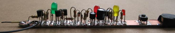
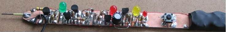
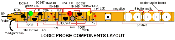
The Logic Probe can be built on a small strip of bare copper clad PC
board, 1cm wide x 18cm long.
All you have to do is cut across the board with a triangular file or saw
or blade to create 3mm wide lands. The parts are soldered to these lands
and after all they have been fitted, short lengths of enamelled wire
join up the negative rail, positive rail and some of the other parts to
complete the circuit.
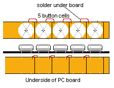
The 5 button cells are held in place with fine tinned copper wire
and the underside of the board is used to create the positive terminal
for each cell.
The photos show how the parts are placed on the board and its a very
good construction-exercise.
This type of construction is quite normal for high frequency circuits
and is still used in many amateur transmitters.
It has some advantages. It takes up less space,
the board can be long and very narrow to produce the shape of a "pen,"
you can use reclaimed components from your "parts-box," and you can use
surface-mount components from old computer modules. But the
best part - it is cheap.
Here is the layout of the prototype: