|
HIGH
and LOW IMPEDANCE CIRCUITS |
|
WHY? Why do we need to know about IMPEDANCE? Impedance is the word we use to explain how a complex circuit works. A "complex" circuit is one that includes components such as inductors, capacitors, chips, transistors, motors and other items, including resistors. You cannot use the word RESISTANCE as resistance applies to a simple circuit such as a torch. The term IMPEDANCE lets you explain how much current is flowing, as well as other features. It's a complex term but we will cover it in a simple way. If you want to see its complexity, go to these links: Reactance Capacitive Reactance Capacitive Reactance Calculator Inductive Reactance The term IMPEDANCE is surrounded with equations. Of course you can use them, but they don't EXPLAIN anything. You need to UNDERSTAND the term before putting it into an equation and to do this, you need to "see" a circuit in operation. Then you will be able to work out things like: current consumption; effects of a spike, resonant frequency, etc. Nearly every circuit consists of resistors, capacitors, transistors, chips etc and they all fall into the category of a "complex circuit" (complex - meaning the mixture of a number of different components). Thus you will need to use the term IMPEDANCE when describing almost every circuit. |
Before we start, we need to know what we mean by
"circuit" and "impedance."
A circuit is almost any component and its surrounding wiring. A circuit
may be as simple as a globe, length of wire and a switch. It may be an oscillator
circuit consisting of 15 components, or it may be the power supply for a 15 layer PC board.
A circuit is not just a globe or resistor. We call these
components.
A circuit must include
the wiring as this can create problems such as
picking up spikes or reduce the current-flow. And when the circuit contains more than one component
plus trackwork on a PC board, the situation becomes very complex.
The following figure shows three typical circuits:
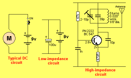
Fig 1: Some typical
circuits.
WHAT IS IMPEDANCE?
IMPEDANCE is very similar to RESISTANCE. They both have the
same unit: OHM.
A
low
impedance
circuit
is very similar to saying a low
resistance
circuit
however we use the term impedance because the actual resistance
of the circuit may change according to the
frequency at which it is operating. The term impedance takes this
into account.
If the circuit only operates at DC (this
is a steady state such as a globe in a torch and is equal to a frequency
of 0Hz - zero cycles per second) we can use the term
resistance. But most circuits have waveforms and sometimes noise
or ripple, so the term IMPEDANCE is used.
The term LOW IMPEDANCE and HIGH IMPEDANCE is a relative term. If we are
working on a one-watt amplifier circuit for example, a low impedance may
be 10 ohms or one ohm. If we are working on a 1,000 watt amplifier, a low
impedance may be 0.1ohms or 0.001 ohms!
A high impedance in an automotive circuit may be 100 ohms or 1k, whereas
a high impedance in an oscillator circuit may be 100k. A high impedance
OP-AMP or CMOS circuit may be 1M or 10M.
The following figure shows some stages we will be covering (also called "gates" or "blocks.").
Each line has been identified as "high-impedance" or "low-impedance."
An output line is identified as low impedance as it is either HIGH or LOW
(the two stages of a digital gate) and the line will be held in this state
by the action of a transistor (or transistors) inside the chip. If the
impedance of the line is measured (in either state), it will be LOW.
An input line is classified as a high-impedance line. But if it is directly
connected to the output of a gate, it will measure as a LOW-impedance line.
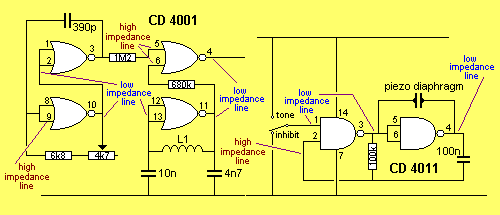
Fig 2: Some high and low impedance
"blocks."
We show how to test 3 of them.
One of the reasons we use the term "IMPEDANCE" is to remind
you that the circuit has a particular feature (measured in ohms) at a
particular frequency.
We also use the term "impedance" when non-resistive components are
involved in working out the final value - such as capacitors (and
electrolytics) as these have different effects at different frequencies.
For instance, a power supply must have a LOW IMPEDANCE so that the output
voltage is maintained over its full range of current. That's why the output
nearly always contains a large-value electrolytic.
The circuitry in a CMOS project must be HIGH IMPEDANCE if you want
it to consume the lowest current. The whole purpose of using CMOS
technology is to consume the lowest current.
With any circuit, there are three things you need to know:
1. Is the circuit HIGH IMPEDANCE or LOW IMPEDANCE?
2. How to test a HIGH or LOW IMPEDANCE circuit.
3. How to keep a circuit HIGH IMPEDANCE or LOW IMPEDANCE -
when designing or
modifying it.
1. IS A
CIRCUIT HIGH OR LOW IMPEDANCE?
We have already covered this point.
Impedance is a relative term. An engineer who designs CMOS projects will
consider any line less than 1M as low impedance. An audio technician will
consider any speaker-line above 1 ohm as high impedance!
2. TESTING
We will take "stages" or "blocks" from
the circuits above and explain how to test them.
FIRST CIRCUIT:
The first "block" or "gate" to be discussed is shown in fig 3 below. Both inputs of the gate are high impedance. These
high-impedance lines are arrowed.
Since this is a digital circuit (the voltages on the inputs will be
LOW (very near 0v) or HIGH (very near rail voltage). It is
very easy to measure the voltage on a digital line and determine if the circuit is
working - providing the measuring equipment does not upset the
voltage.
The output of the NOR
Gate is HIGH when both inputs are LOW.
Suppose output pin 4 is not changing.
The reason may be a faulty chip - change the chip.
If the fault still persists, here is the procedure for testing the circuit:
When pin 3 goes HIGH, the voltage is passed to pin 5 via a
1M2 resistor.
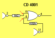
Fig 3: A high-impedance circuit
The 1M2 is not needed as pin 5 is a high impedance input and is capable of
receiving a voltage equal to that delivered by pin 3. The 1M2 serves NO
PURPOSE. It can be removed.
The person who designed the
circuit did not
go though it and work out if each component is absolutely necessary. This
is one of the final points we teach when designing a circuit.
If you are not sure about the effect of removing a resistor, it can be
replaced with a lower value, such as 10k. This is called a "safety resistor" as it will prevent
any damage, in case the output and input do not match up
perfectly. If the 10k does not affect the circuit it can be replaced with
1k and finally removed altogether.
The 680k can also be replaced with a 10k resistor and finally removed.
This will reduce the input impedance of the gate to a "low impedance" state
and allow you to test the inputs. The following diagram shows how to reduce
the value of a resistor while testing the circuit to see if the change has
made any difference in the operation. Before removing a resistor
completely, you need to take a current reading through the resistor. If no
current flows (i.e: no voltage is developed across the resistor) it can be
removed safely.
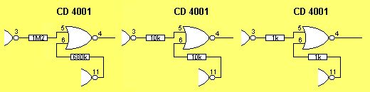
Fig 4: Reducing the value of the resistors
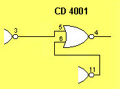
Fig 5: Removing the resistors
to
produce low-impedance inputs
With the two resistors removed, the waveform on the inputs can be probed with a CRO. The waveforms will be a "square wave." This means the rise and fall will be very fast, with a flat top and bottom to the shape. The excursions will be as close as possible to the positive rail and 0v rail. The waveforms will not be "square" but "rectangular." The term "square wave" simply means the sides are parallel, the top and bottom are flat and the corners are sharp. (There are waveshapes such as sinusoidal, triangular and exponential to describe other waveforms).
Fig 6: The waveforms on the
gate.
The input lines are now low-impedance and the CRO will not load the inputs
of the gate. The waveforms will be as shown in figure 6. If a waveform has
any of the characteristics shown in figure 7, the gate will not detect the
change from a low-to-high or high-to-low and the output will not change. In
Fig 7, the first waveform does not rise high enough for the input of a gate
to detect a HIGH. The waveform must rise to about 55% of rail voltage to be
detected by a digital gate as a HIGH. If the gate is a Schmitt Trigger, the
waveform must rise above 66% of rail voltage.
The second
waveform does not fall below 45% to be detected by a digital gate as a LOW
and if the gate is a Schmitt Trigger, the waveform must fall below 33% of rail voltage
to be detected as a LOW. To make sure a waveform is detected, it must be as
large as possible.
Fig 7: Faulty waveforms -
these
waveforms will not trigger an input
SECOND CIRCUIT:
The next circuit to be discussed is an oscillator made up of
a NOR gate and a
coil. The input (pins 12 and 13
are connected together) takes time to rise and fall due to the
charging/discharging of the 10n capacitor. The frequency is also set by the
waveform produced by the inductor L1. The waveform adds or detracts from
the voltage produced by pin 11 and this alters the charge-time for the 10n
and thus alters the frequency of the circuit. The circuit is self-starting as the
NOR gate is wired as an inverter and when the input is low, the output is
high. This high is transferred to the input to change the state of the
gate. The 10n capacitor slows down the time for the input to change state
and this creates the frequency for the circuit (as well as the effect of
the waveform from the inductor - as mentioned above). If the
inductance of L1 is changed (by placing a metal object near the coil) the
amplitude produced by the coil is altered.
Fig 8: A difficult circuit to test
If the output of the circuit above does not produce a waveform as shown in fig 9,
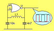
Fig 9: The output of the
gate
the fault could lie in the gate, the coil (inductor L1), the 10n capacitor,
the 4n7 capacitor, or a dry joint on the printed circuit board.
The first thing to do is build the circuit with new components on a
bread-board or a "birds-nest," to prove the circuit will work. You can
then swap the 3 components and the chip from the printed circuit board to
the birds-nest, one component at a time, to locate the faulty item. If the circuit still does not work, the fault will lie in
the track-work on the printed circuit board or the voltage to the chip.
You cannot test any of the circuit with a multimeter as the input and
output is low-impedance and the circuit is oscillating at a frequency from
10kHz to 150kHz, depending on the inductance of L1 and the effect of both
capacitors. This makes resistance
tests impossible to provide any answers and you have to use the
"comparison" approach of transferring the components.
A CRO placed on the output will show a waveform similar to that in fig 9.
The sharpness of the waveform will be modified by the effect of the 4n7
capacitor and the inductor, as well as the 10n capacitor.
THIRD CIRCUIT:
The third circuit is shown in Fig:10. It drives a piezo diaphragm. There are two types of piezo's. One
has the driving circuit included in the plastic case and will operate
from a DC supply. This is sometimes called a piezo sounder, piezo buzzer or
piezo siren. The other type has only a diaphragm and requires a
driving voltage (AC voltage). This is the type we are using.
The second gate in Fig: 10 is a NAND gate wired as an INVERTER. The two
gates form an oscillator with the 100k and 100n as timing components.
Both the input and output of the second gate are low impedance and the piezo
diaphragm is driven from the output of the first gate and also the
second gate. These two lines are out-of-phase and the diaphragm sees a
voltage in one direction and then the other.
The change in voltage "dishes" the diaphragm in one direction,
then the other
to create sound.
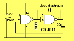
Fig 10: The
oscillator circuit
When input pin 1 is taken HIGH, the first NAND gate will function as an
INVERTER - the output will always be the opposite of the input. This means the HIGH output
on pin 3 will pass to input pin 2 via the 100k
resistor. This will make the output LOW via the action of the gate to create a HIGH
output. Normally, the gate will oscillate very
quickly when the output is connected to the input. But the circuit contains a 100n on input pin 2. This capacitor slows down the rise
and fall on the input pin and creates the frequency for the oscillator.
If the circuit does not work, you can take pin 2 HIGH via a jumper lead and
measure pin 3 to see if it is LOW. Take pin 2 LOW and see if pin 3 is
HIGH.
This is called "forcing the circuit to work."
FOURTH CIRCUIT:
The next discussion is a high-impedance circuit:
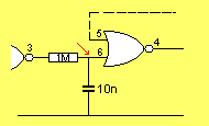
Fig 11: A high-impedance input
The waveform on pin 6 will depend on the frequency of the signal on pin 3 as well as the shape of the signal. If the frequency is too high or the Mark-Space ratio is not suitable, the 10n will not have sufficient time to charge (or discharge) and thus the voltage level will not be sufficient to be detected by the gate. The following diagrams show the results of two unsuitable waveforms and a correct waveform:
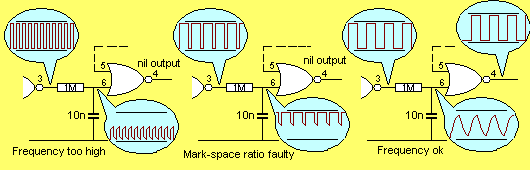
Fig 12:
Detecting different waveforms
In the third circuit of Fig:12, the frequency is ok and the waveform from pin 3
is detected by pin 6. The waveform is only just sufficient to be detected by the gate.
If you place a CRO on pin 6, the added resistance (impedance) of the CRO
may reduce the waveform and prevent pin 6 detecting the signal. This is
shown in fig 13:
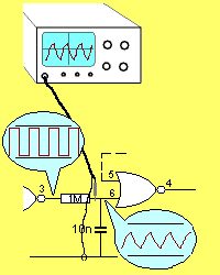
Fig 13: The load of the CRO will
"freeze" the circuit.
The CRO has a resistance (impedance) of approx 1M and this creates a voltage divider. The voltage on the 10n will
never rise above half-rail voltage and the gate will not detect a high.
Thus the output
of the gate will not change.
The CRO will "freeze" the operation of the circuit.
FIFTH CIRCUIT:
Fig 14 is a power supply made up of a battery and capacitor (or
electrolytic).
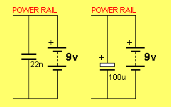
Fig 14: Low-impedance power
supply
The purpose of a capacitor (or electrolytic) across a battery is to improve
(increase) the current on the POWER RAIL while keeping the voltage on the
POWER RAIL as high as possible.
It effectively turns an "old" battery into a "new" battery.
The additional current comes from the energy stored in the capacitor and this can only be delivered in the form of "spikes" or "bursts"
as the capacitor does not hold a lot of energy.
All batteries have a limited life. As they get "used" the output voltage
reduces. This is due to microscopic bubbles of gas developing inside the
cell and increasing the resistance as well as the active chemicals being converted to inactive
compounds that have a higher resistance and this does two things:
The output voltage of the cell reduces and the current capability is
reduced.
A 9v battery is one of the best examples of this problem. It contains 6
cells. If an old battery is tested, the output voltage may be say 8v. This
reading does not tell you anything. It does not tell you if the battery is
old, very old or almost completely dead. You cannot test it by taking a
voltage reading.
A piece of equipment uses a battery entirely differently to a
"test."
Equipment requires current in bursts (such as the audio from a radio or
beeps from a gold detector).
An "old" battery cannot supply "bursts of current" (due to the increased
internal resistance of each cell) and the voltage on the "supply rail"
reduces. The lower voltage causes the circuit to draw a lower current and
on top of this, the battery can only supply a low current.
This creates distortion or a number of other annoying faults.
To reduce the problem, a capacitor or electrolytic is placed across the
supply rails.
The value of the capacitor can be worked out by trial and error. Simply
select a high value and view the waveform of the supply rail on a CRO.
Reduce the value until the waveform become noticeable (distorted audio etc)
or the operation of the circuit is upset.
The addition of the capacitor is said to "tighten up the rails" or "reduce
the impedance of the supply rails" - the circuit becomes LOW IMPEDANCE.
This type of low impedance circuit is not easy to measure. The
capacitor provides an "effect" rather than a measurable impedance
and you can readily hear the "effect" by listening to an audio amplifier.
The effect of the electrolytic is to create a 9v battery capable of
delivering a high current.
The battery charges the electrolytic when the current required by the
circuit is low and delivers it in a burst when needed.
SIXTH CIRCUIT:
Fig 15 shows a simple transistor stage.
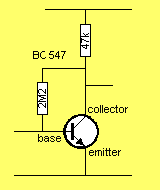
Fig 15: A simple transistor stage
There are three areas where impedance measurements can be taken:
1. Across the input terminals - see Fig 16.
2. Across the biasing resistor, and
3. Across the load:
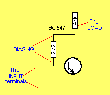
Fig 16: The 3 areas under
discussion
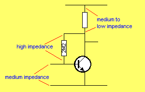
Fig 17: Impedance values of
a transistor stage.
If you measure any of the above values with a multimeter, you will not get a
correct reading because you are taking a resistance-reading. We are talking
about impedance
values.
One of the reasons you cannot measure the resistance of the INPUT terminals
is due to the diode-junction between the base and emitter leads. It will
measure high in one direction and very low in the other direction.
|
MEASURING A TRANSISTOR WITH A MULTIMETER The low reading across two terminals of a transistor is not a resistance value. The multimeter has a 3v battery inside it to deliver a current through the probes. With ALL resistance measurements, a multimeter is actually reading a value of current-flow and interprets this as a resistance reading. The base-emitter junction of a transistor, for example, has a "natural" or "characteristic" voltage-drop of about 0.7v across it and this voltage is being removed from the 3v supply in the multimeter so the final reading is actually the current-limiting components in the meter delivering a current to deflect the needle. |
Rather than talk about exact values of impedance, we will show how to
increase the value of impedance of the input of a transistor stage.
1.
Adding
an emitter resistor will increase the input impedance:
The input impedance of Fig 18 has increased by the value of the emitter
resistor.
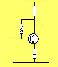
Fig 18: The emitter resistor has
increased the input impedance.
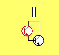
Fig 19: The red transistor has
increased the input impedance 100 times!
2.
When two transistors are placed on top of each other as shown in Fig 19,
they form a combination called a SUPER ALPHA PAIR. In our
discussion, the red transistor is the added component and it increases the
input impedance 100 times or more - the increase is equal to the gain of the red
transistor.
The input impedance can be 100k - 300k. This value cannot be
measured with a multimeter. The only way it can be appreciated is
when the two transistors are connected to a circuit. The input will put very little load on
anything it is connected to (such as an electrolytic) and it is sometimes
used as a timing circuit to detect the discharge of a capacitor.
Or it can be placed across a device (also called a generator, or
transducer) that produces a very small current. This type of transducer is
called a high-impedance device and it needs to be connected to a
high-impedance detector (the circuit above) so that the current or waveform
it produces is not attenuated (reduced).
Matching the output characteristics of a transducer to a circuit or
"building block" is one of the most important concepts in electronics. The
performance of a circuit can increase 10 times or more when
correct matching is employed.
BIASING
The transistor in Fig: 20 is biased via a 2M2 resistor. This
is called the "biasing area" of the stage and is a high impedance area.
You cannot place a multimeter across the 2M2 as this will upset the
biasing of the stage.
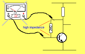
Fig 20: The biasing of the
transistor
You cannot use a multimeter to measure the biasing resistor
The only way to work on the biasing is to fit a resistor and
observe the results. Listen to the output, measure
the voltage on the collector or place a CRO on the collector and view
the signal.
The LOAD of a stage is the value of the LOAD RESISTOR as shown in Fig: 21.
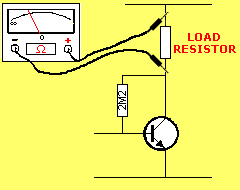
Fig 21: The load of a stage
Measurement must be made with the supply OFF
If the stage is connected to a following stage as showing in Fig: 22, the LOAD for the first stage is a complex value to determine.
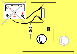
Fig 22: The LOAD of a stage
can include
the effect from the stage that follows
The LOAD cannot be measured with a multimeter
The only way to select a value for the LOAD RESISTOR is to try different
values by EXPERIMENTATION. Before deciding on a final value, try a larger value and note the
effect. Then try a smaller value and document the effect.
Make sure the final value is the most suitable for the
application.
Some of the features to take into consideration are: lowest current
consumption, highest output and lowest distortion.
The next section in this course will cover MATCHING STAGES. This is one of
the most important concepts in electronics.
You must be able to "see" or "visualize" the output impedance of a device
such as a transistor and the impedance of the item it is being connected
to. You need to get the matching as close as possible so the transfer of
information is the highest.