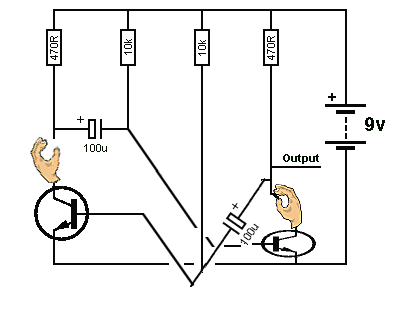
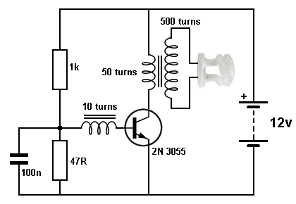
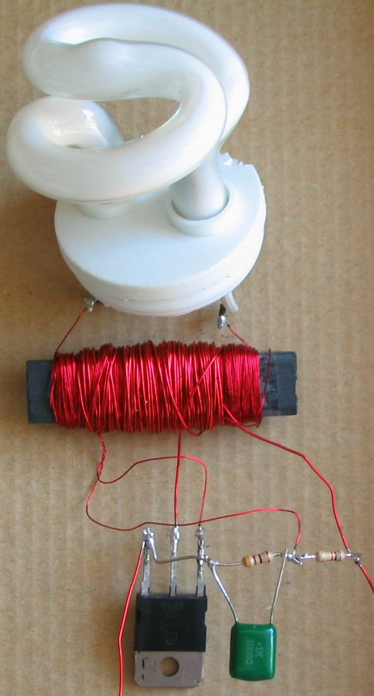
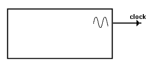
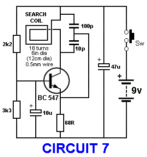
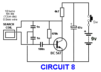
FEEDBACK in an OSCILLATOR
Only a small portion of the OUTPUT SIGNAL
in an oscillator is fed back to a
previous part of the circuit. It only needs a small amount to
keep the oscillator working.
This is generally done with a capacitor. A capacitor will
deliver a signal while preventing the voltage on
the output from being passed to the input of the oscillator - it
only passes the signal. The voltage on the output is much
higher than the voltage on the input and these two values need
to be separated and only the signal (the waveform) passed from the
output to the input.
A capacitor will ATTENUATE (reduce the amplitude) of the
output signal and only deliver a "miniature version." It does
this because the capacitor charges during the time when the
signal is rising and the voltage developed across the capacitor
is subtracted from the signal being delivered. That's why the
value of the capacitor is important. By selecting a smaller
value, a smaller waveform is passed to the small-signal section
of the circuit.
The "signal" is a rising and falling voltage and this voltage must
ASSIST the rising and falling voltage on the input.
This signal is called a POSITIVE FEEDBACK signal.
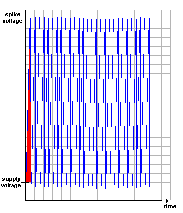
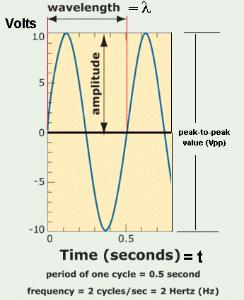
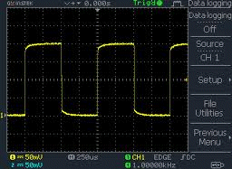
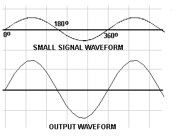
A waveform is a signal or a line drawn on graph paper or a
"trace" on a Cathode Ray Oscilloscope that generally
starts at the 0v rail and rises to a peak. It then decreases to
the 0v rail. It may also pass through the 0v rail and travel in
the negative direction to the same negative amplitude of the peak. It
then travels to the 0v rail to complete ONE CYCLE.
A complete cycle is drawn on GRAPH PAPER with 0° at the
beginning of the cycle and 360° at the
end, so you can work out the various parts of the waveform
for positive or negative feedback. This allows us to talk about what is happening at 90°
or 180° or at any other part of the graph.
It doesn't matter if the waveform is a sine-wave, square-wave
or triangular, it can be drawn on a grid with the start of the wave
at 0° and the end at
360°.
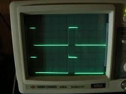
To work out if the output waveform will deliver a Positive or
Negative feedback signal, a second graph needs to be drawn. The second graph is drawn below the
first graph and a ruler is placed vertically to align the
two graphs. You can then see what is happening at one point on
the top graph and compare it to the signal on the lower graph.
These graphs will need to come from the traces on a dual-race
Cathode Ray Oscilloscope.
Make the top graph the "small-signal" graph and lower graph from
the output of the oscillator.
Move a perpendicular ruler across the graph and watch the rise of the
small-signal. If the "small-signal" is rising and the output signal
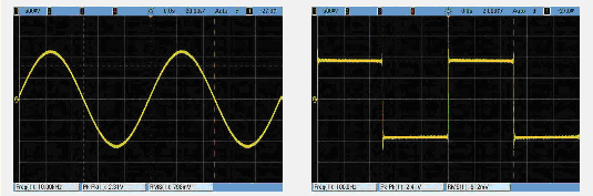
is rising, the result will be POSITIVE FEEDBACK.
The output signal has a high amplitude and
is above the "small-signal"
will "pull-up" (assist - increase) the
small signal and thus keep the
oscillator working
IN PHASE
On the graph you can see the signal is rising
from the 0v rail at 0°.
The graph continues and at
360° the signal will rise again from the 0v rail
to start the next cycle.
This means the signal at 0°
and 360° are doing the SAME THING - it is rising.
These two parts of the graph are IN PHASE. In other words both lines on the
graph are identical (in the way they are moving UP) - one line can be placed on top of the other
and they are the same.
OUT OF PHASE
The signal at 0° is rising and the signal at 180° is
falling.
This is called OUT OF PHASE - the two lines on the graph
are not going in the same "up"
direction.
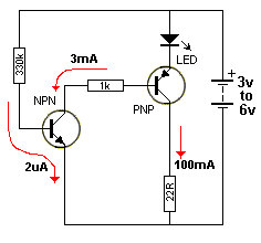
There are two types of feedback signals in electronics.
POSITIVE and NEGATIVE.
If the signal strengthens the signal
in the "small-signal" section, it is called POSITIVE FEEDBACK
and is IN PHASE. This means the two signals are rising at
the same time and on the graph they are
360° apart, but in reality they are
rising AT THE SAME TIME.
If the output signal REDUCES the waveform of the
small-signal, it is called NEGATIVE FEEDBACK and the
signals are NOT IN PHASE. On the graph they are
180° apart but in real-time one
signal is rising and the other is falling AT THE SAME TIME.
A POSITIVE FEEDBACK
signal
ASSISTS the small-signal.
A NEGATIVE FEEDBACK signal reduces the amplitude
of the small-signal.
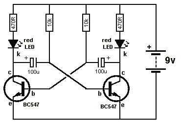
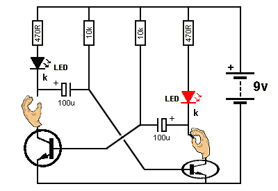
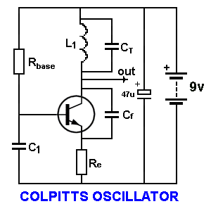
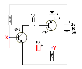
Another name for POSITIVE FEEDBACK
is BOOTSTRAPPING. A large percentage of the output is
intentionally passed back to the front-end to assist the
incoming signal. The result is a very large output. See
Stereo VU Meter project for a Bootstrap Circuit. The same
circuit is also
here. Another circuit showing the effect of Positive
Feedback is the
Clap Switch. The effect can also be called REGENERATION,
where a small change is passed to an output then back to the
input to create a larger change his circulated around the two
stages until the are both turned ON fully.
Positive Feedback and Bootstrapping can have a very large effect
on the incoming signal and increase the output to a point where
clipping or distortion occurs as shown in the Clap Switch
circuit. The two components creating the Positive Feedback are
the 100u and 100k in series.
Another name for NEGATIVE FEEDBACK
is ERROR SIGNAL or ERROR FEEDBACK. If the output
contains distortion or spikes, these parts of the waveform will
not be present in the small-signal waveform. By sending the
output back to the small-signal section and combining the two
waveforms, the Negative Feedback signal will have an effect on
reducing those parts of the waveform that are different. The
peaks or bumps will be reduced and these are the parts of the
waveform called "distortion."
PHASE REVERSAL
A rising signal on the base of a common emitter transistor will
produce a falling signal on the collector. This has been covered
in the section:
The
Transistor.
This is called PHASE REVERSAL or SIGNAL REVERSAL.
In other words the signal is OUT OF PHASE by
180°. This will produce a
NEGATIVE FEEDBACK signal.
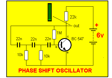
To produce a POSITIVE FEEDBACK
signal, the signal must be at 0°
and 360° on the graph so they are IN PHASE.
How do you get a signal that is 360° out-of-phase?
Here is the answer:
A second common emitter stage will produce 180°
phase-shift, making a total of 360° phase-shift to produce
a POSITIVE FEEDBACK
signal.
In other words, two stages of reversal is the
same as non-reversal. 360° phase-shift is the same as 0°
phase-shift.
PHASE-SHIFT is NOT DELAY. Phase-shifting simply
means the incoming signal has a slightly
higher amplitude and is rising at the same rate to provide Positive Feedback. Or the incoming signal may
traveling in the opposite direction to provide Negative
Feedback. Negative feedback simply means the incoming signal is
"pushing down" on the small signal and reducing its amplitude.
The incoming signal will have more effect on the peaks and
that's how distortion is reduced or removed.
When looking at the waveforms for FEEDBACK, we are not
interested in FREQUENCY or PERIOD. We are just looking at the
timing of one waveform and comparing it to another to achieve
Positive or Negative feedback.
"Timing" means the relative position of one wave on the graph,
then looking at the other wave to see if it ASSISTING or
CANCELING the "small-signal." We have already motioned above,
how to work out how the incoming waveform is affecting the
"small-signal."
That's why we don't have a TIME SCALE on the graph.
The waveforms we are studying are called PERIODIC WAVEFORMS. In
other words they repeat. The waveform can be any shape or size,
as long as the next cycle is identical to the previous.
An example of a non-periodic waveform is speech. Each cycle is
slightly different to the previous. However a tone or whistle is
periodic because each wave is very nearly identical to the
previous.
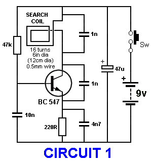
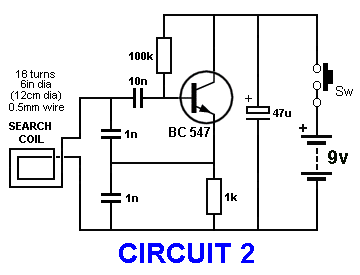
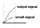
The easiest way to create a Positive or Negative feedback signal
is to experiment with an actual circuit.
The value of the capacitor is VERY CRITICAL. It may be 10p or as
high as 10u. Sometimes a resistor can be added in series with
the capacitor. This will alter the "timing" by delaying the
effect of the capacitor and since the combination of the two
values will produce an enormous number of possibilities.
We explained above, the capacitor will pass nearly all the
amplitude of the output waveform to the small-signal section or
only a small percentage of the amplitude, depending on its
value.
If it is small, it will get charged during the transfer and most
of the amplitude will be lost (ATTENUATED). The actual
percentage transferred will also depend on the frequency as the
capacitor will not be able to charge very much when the
frequency is very high. At low frequency, the same-value
capacitor will charge to a higher voltage because it has more
time to charge.
To see exactly what is happening, you need a need a piece of
test equipment.
That's why we use a CRO
(Cathode Ray Oscilloscope). It has a screen and you can watch
what happens when you change the value of a component.
Sometimes, a slight change in the value of a component will
alter the operation of the circuit considerably and that's why
you cannot predict what will happen or use any form of
simulation software. You MUST build a circuit and test it. |