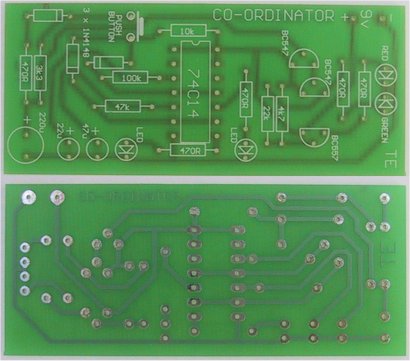
CO-ORDINATOR
A game of skill and patience
This project combines some of the components and building blocks we have covered in the courses in this e-magazine. It's a game of skill that tests your reaction-time and patience.
Patience, because a certain condition appears on the indicator LEDs, only every few seconds and it corresponds to them both being OFF.
When they are both off, you must press the control button and this supplies a little energy to a reservoir electrolytic. The voltage on this electro is detected by a high impedance amplifier and the result is shown on a "LED-Pair.' As the voltage rises, one of the LEDs in this pair gradually dims and its brightness is transferred to a LED of the opposite colour.
This process is very gradual and may take up to 20 to 30 pushes. But if your timing is out, all the progress of 20 pushes will be lost to the discharge circuit.
The time when it is safe to press and NOT press is very abrupt and you have to be very careful not to extend into the “forbidden" zone.
|
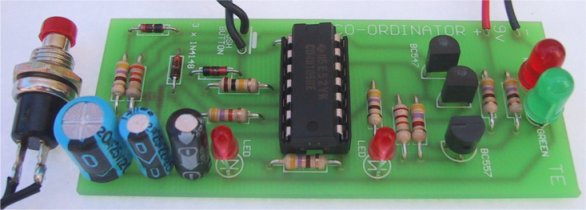
The completed Co-ordinator, showing the placement of the components |
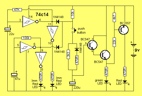
| The Co-ordinator Circuit |
The first building block is the low frequency oscillator, of which there are two. Each oscillator operates independently and its flash rate is indicated on a LED. The LED is buffered by an inverter to use the gates in the chip.
This arrangement also allows the output of the oscillator to rise to full voltage and allow the capacitor to charge. Any loading of the output of the oscillator does affect charging and if it does not rise to 66% of rail voltage, the oscillator will not operate.
The value of the timing components in each oscillator is not very important and we have chosen 47k and 22u for one set and 100k and 47u for the other. This will give a flash rate of about 4:1 and means the two output LEDs are both OFF for a very small fraction of the time.
The next block is the GATE, made up of two signal diodes and a 10k resistor. This forms an AND gate and operates as follows: The circuit requires a HIGH on the end of the 10k resistor to charge the reservoir electrolytic and this is available ONLY when the cathode of both diodes is HIGH.
This condition corresponds to both LEDs being OFF and thus the circuit is designed around the OFF state.
When the output of both oscillators is HIGH, the charging path for the electrolytic is via the 10k and 3k3 resistors and during the short period of time when this occurs, the button should be pressed. When either oscillator goes LOW, it brings the discharge path into operation.
The discharge path is made up of a 470R and signal diode. This path has a much lower impedance than the charge path (the 3k3 resistor) and thus most of the good work done during the charging will be lost by one false move.
During charging, the diode (in series with the 470R) forms a 'blocking' effect and does not play any part in the charging.
Next we come to the high impedance DETECTOR circuit. It is actually an emitter-follower arrangement, designed to turn ON one of the indicator LEDs. The question we ask is "Why use two piggybacked transistors?" In simple terms, the answer is to keep the LED illuminated between presses of the switch. This block is a good example of how a transistor operates. It shows that a current is required by the base, for it to supply collector-emitter current.
If we remove the top transistor and connect the base of the lower to the electrolytic, the LED would gradually dim between pushes of the switch. This is because the base requires current for the transistor to drive the LED and it draws on the electrolytic for this energy. The voltage across the electrolytic would gradually fall and the effect of the game would be lost.
By placing another transistor across the first, the current drawn from the electrolytic is reduced by much as 1/200th and the brightness is maintained.
This arrangement is called a SUPER ALPHA pair or SUPER TRANSISTOR as the gain of the transistors is multiplied together to produce an arrangement similar to a single transistor with enormous gain.
The output of this stage is taken to a common-emitter arrangement (for a PNP transistor) in which the load is in the collector. This stage turns off when the previous stage turns ON.
This is the entire circuit. It consists of one chip, 3 transistors, 4 indicating LEDs and a few resistors, diodes and capacitors. The circuit is supplied by 9v and is designed to accept a tri-coloured LED or a red and green LED in the output.
Building the project will help you understand the circuit a lot more and bring together the theory we have covered.
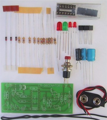
| Co-ordinator kit contents |
|
PARTS LIST |
|
5 - 470R 1 - 3k3 1 - 4k7 1 - 10k 1 - 22k 1 - 47k 1 - 100k 1 - 22u 16v electrolytic 1 - 47u 16v electrolytic 1 - 220u 16v electrolytic 3 - 1N4148 diodes 2 - BC 547 transistors 1 - BC 557 transistor 2 - 3mm red LEDs 1 - 5mm red LED 1 - 5mm green LED 1 - 74c14 lC 1 - push switch 1 - 9v battery snap 1 - 14 pin IC socket 1 - 20cm hook-up flex 1 - CO-ORDINATOR PC BOARD |
ASSEMBLY
Begin construction with the smallest components. They are easier to fit when no other components are on the board. Begin at one end and fit the 3 diodes and 9 resistors. The 3 diodes must be fitted so that the cathode end (as indicated by a black band around one end) goes over the 'bar or line' shown on the overlay.
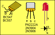
Next fit the 3 transistors. Two are NPN and will be BC 548 or 2N 2222. The other transistor is PNP and will be BC 558 or 2N 3906.
After this we fit the 4 LEDs. The two mini LEDs are 3mm and the cathode lead
must be fitted near the edge of the board. You have a choice of output LED. It can
be either a 5mm red LED and green LED or a single tri-coloured LED. Either of
these arrangements can be fitted to the board. But NOT both.
Fit the IC socket so that pin 1 identification (a cut corner on the socket
or a notch at one end) covers the dot on the PC board. This makes it easier to
insert the IC correctly, when all the other components have been added. Solder
the 3 electrolytics so that the positive leads go down the holes marked on the
board. The positive lead is the longer one.
Mount the push switch on leads about 10cm long and solder them to the board
at locations marked 'PCB.'
Finally add the battery snap, push the IC into the socket and the project is
ready for testing.
TESTING
When the power is applied, the two 3mm LEDs should illuminate with
random
flashing and the red output LED will come on.
The LEDs are controlled by 3 separate sections of the circuit and if any do
not work, you should go directly to the section responsible.
If the left-hand mini LED does not flash, the circuit components to check
are: 100k and 47u electrolytic. If the right-hand mini LED does not flash, the
47k and 22u electrolytic should be checked. The fault could also be the chip.
If the 5mm red LED does not come on, the fault will lie in the BC 557 and/or
biasing components, comprising the 4k7, 22k, 470R and the green LED.
Try your friends with the co-ordinator. Those who play video games will have
a good sense of judgment and get the LEDs to change without much difficulty.
There is a secret way of getting the circuit to charge the electrolytic without
the need for any skill. We call it the test' mode but you can call it the
'cheat' mode.
Place a diode across the switch so that the cathode faces the 3k3. This will
cause the electrolytic to charge every time the outputs are HIGH (via the 10k
and 3k3) and will not discharge when the outputs are LOW. And you don't have to
push the switch!
You can add a secret switch and show how clever you are!