
Index
Pages: 1 to 21
Pages:
22 to 41
Pages:
42 to 62
Pages:
63 to 85
INTRODUCTION
Data Book 1
comes in 4 sections for easy downloading.
Each file is approx 1MB
and
contains lots of handy information to help you understand
electronics, plus circuits and ideas.
Data Book 1
is also available for viewing on-line:
Data Book 1 Pages 1 - 21
Data Book 1 Pages 22 - 41
Data Book 1 Pages 42 - 61
Data Book 1 Pages 62 - 85
The pages can be printed and collated into a book for easy
reference.
More circuits and projects can be found on TALKING ELECTRONICS
website:
http://www.talkingelectronics.com
Colin Mitchell
talking@tpg.com.au
Tel: 0417 329 788
|
CONTENTS |
|||
|
|
|
|
|
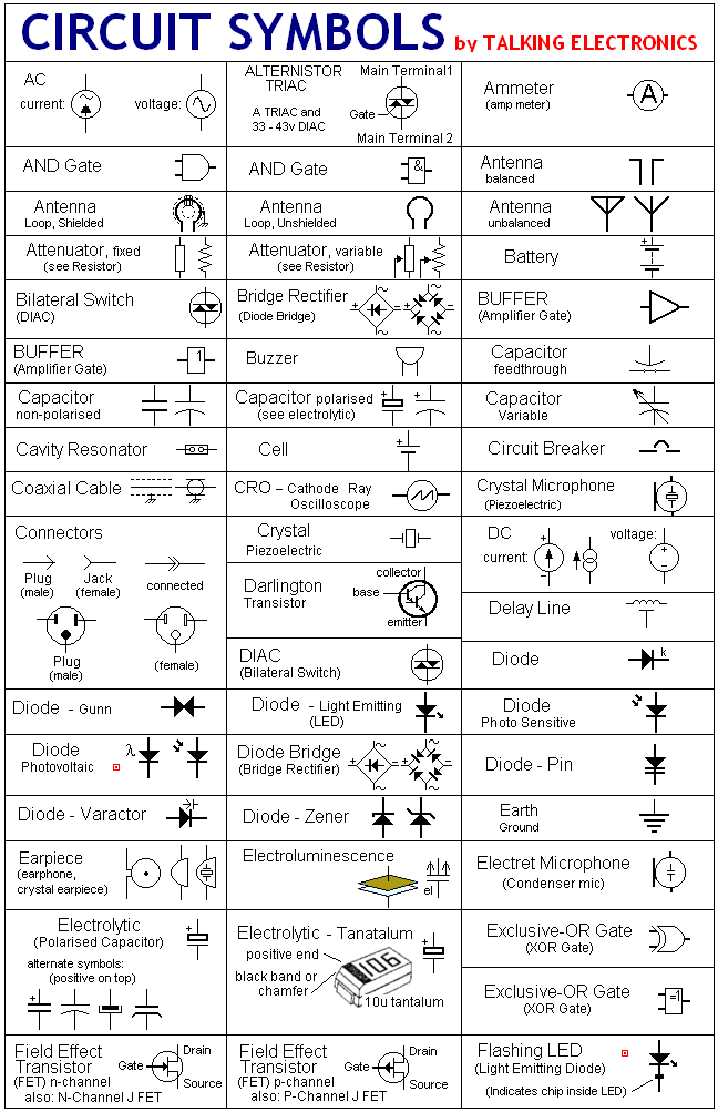
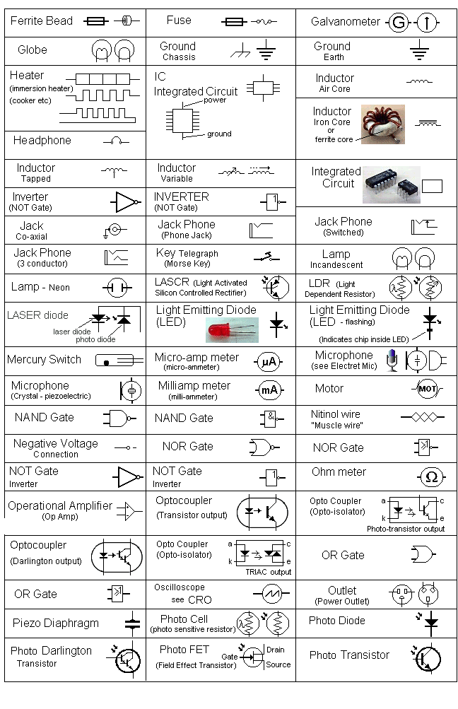
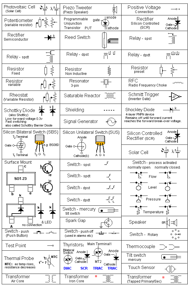
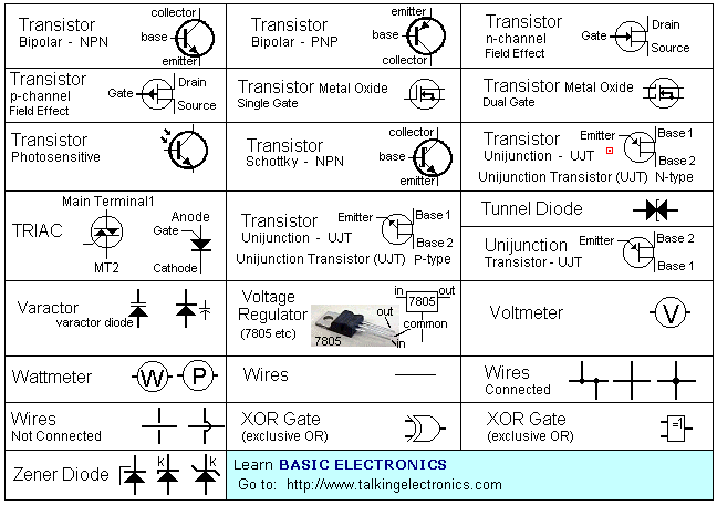
Circuit Symbols
The list above
covers almost every symbol you will find on an electronic circuit
diagram. It allows you to identify a symbol and also draw circuits.
It is a handy reference and has some symbols that have never had a
symbol before, such as a Flashing LED and electroluminescence panel.
Once you have identified a symbol on a diagram you will need to
refer to specification sheets to identify each lead on the actual
component.
The symbol does not identify the actual pins on the device. It only
shows the component in the circuit and how it is wired to the other
components, such as input line, output, drive lines etc. You cannot
relate the shape or size of the symbol with the component you have
in your hand or on the circuit-board.
Sometimes a component is drawn with each pin in the same place as on
the chip etc. But this is rarely the case.
Most often there is no relationship between the position of the
lines on the circuit and the pins on the component.
That’s what makes reading a circuit so complex.
This is very important to remember with transistors, voltage
regulators, chips and so many other components as the position of
the pins on the symbol are not in the same places as the pins on the
component and sometimes the pins have different functions according
to the manufacturer. Sometimes the pin numbering is different
according to the component, such as positive and negative
regulators.
You must to refer to the manufacturer’s specification sheet to
identify each pin, to be sure you have identified them correctly.
Colin Mitchell
Page 8
1N4001 to 1N4007
Silicon Power Rectifiers
The following
are subminiature general purpose power rectifiers for low power
applications
Electrical Characteristics Specifications
 |
Maximum Full-Cycle Average Voltage Drop @ Forward Current = 1 A 0.8V Maximum
Reverse Current
0.03mA
1N4001
35v
1N4005
420v |
| Instantaneous
Voltage Drop @ forward current = 1 A 1.1v Absolute Maximum Ratings Peak Repetitive Reverse Voltage 1N4001 50V 1N4002 100V 1N4003 200V 1N4004 400V 1N4005 600V 1N4006 800V 1N4007 1000V |
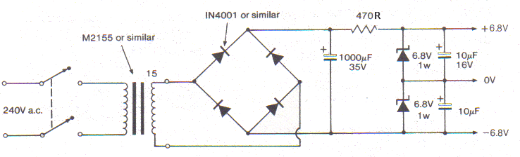
Their value will depend on
the current and the degree of smoothing required.
As a general guide, if the current being drawn from a supply is high,
the size of the smoothing capacitor will need to be large (around 2500uF or larger)
if the hum level is to be
kept down to a respectable level. It must also not be
forgotten that all of these circuits are 'unregulated' i.e. as the load increases
from zero
to maximum the output voltage will drop due to the transformer
voltage dropping under load and losses across the
diodes - and the storage
capacity of smoothing capacitors.
Example
Say for example we want a power
supply to give 9V at 1 A.
We could use a M21 55 transformer which is
rated at 1 A.
If we use a bridge rectifier and the 9V tapping the
output voltage will be:-
VDC= 1.41 XVAC
- 1.41 X9V
=
12.69V
Peak ( 9V at 1A load)
Loading and Nominal Voltage
One thing to be aware of with this type of power supply circuit is the voltages given by the formulas are nominal only. Because the actual output voltage of a transformer varies according to its load, the DC output of the power supply will also vary. As well as this, there is a voltage drop across the diodes which will vary according to load. If you need a very precise voltage, the best solution is to use one of the regulated power supply circuits shown in the zener Diode and Voltage Regulator sections of this ebook. You will see that most regulated circuits use one of the circuits above to produce unregulated DC, then regulate it to a consistent voltage that is independent of the load.
Page 9
OA91 General purpose germanium signal diode
The OA91 is a small signal germanium point contact diode. It is suitable for a wide range of RF detector and small signal rectifying applications.
Specifications
Ip Forward current 50mA
VR Reverse
Voltage 90V Vp,
Forward voltage drop
@ ip = 10mA 1.05V
@lF = 0.1mA 0.1V
Crystal Set
The crystal set consists of a tuned circuit which selects the wanted station or frequency, and a detector, which separates the information (music, speech etc.) from the radio transmission. The audio voltage produced is an exact replica of the sound from the radio station.
The detector diode rectifies the incoming signal,
leaving a half wave radio signal which varies in amplitude with the
audio signal. The fixed capacitor C2 shorts out or 'bypasses'
the RF signal, leaving only the audio.
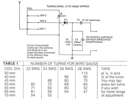
The
circuit below is for a Crystal set using a readily available Ferrite rod
and pre-wound aerial coil.
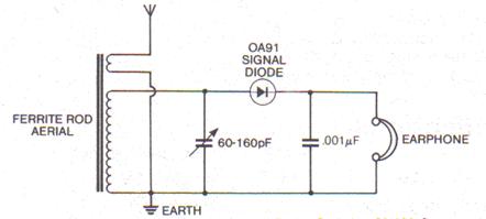
RF Monitor Meter
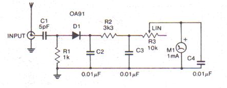 |
The circuit is an RF monitor meter suitable for measuring the strength of a signal from transmitters. You could use it to measure the effectiveness of different antennas for example. It works in much the same way as the crystal set, but without the tuned circuit. The meter M, will indicate the strength of the 'carrier'. Modulation of the carrier i.e. signal on the carrier, will cause the reading to vary. M, is not critical, and any meter of 1mA or better sensitivity will be suitable. |
Page 10
1N4148 Silicon
Signal Diode
The 1N4148 is a general purpose signal diode suitable for a wide range of switching and low power rectifying purposes. It is equivalent to the 1N914.
|
Features • Low Capacitance. 4pF at 0V
•
High breakdown voltage. 100V Specifications
Capacitance VR=0, f=
1MHz 4pF
Rectification Efficiency 2.0V rms. f=100MHz Absolute Maximum Ratings Breakdown Voltage 100V Working Inverse Voltage 75V
DC Forward Current
300mA |
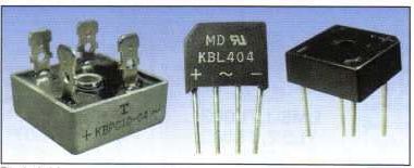 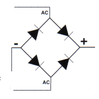 |
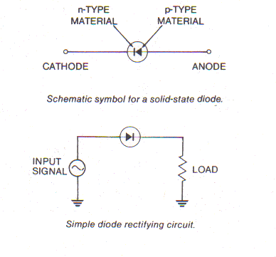
| Diode bridges are a package of four diodes connected in a full wave bridge rectifier configuration. They can be encapsulated in plastic or steel/epoxy cases, and even DIL and surface mount packages for the smaller units. The square metal packages usually have one AC terminal marked, with the other terminal diagonally opposite it. The positive DC terminal is marked, with the negative terminal diagonally opposite it. Plastic square packages often have all terminal markings embossed on the package. In-line plastic packages take up less PCB real estate while still maintaining a reasonable current capacity, and usually have their terminals marked with the AC connections being the inside two leads. | |
Zener Diodes
Zener diodes are used primarily as voltage references.
They are devices which maintain an almost constant voltage
across them despite various changes in circuit conditions.
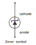 |
Unlike conventional
diodes, zener diodes are deliberately intended to be used with the anode
connected to a negative potential (or 0v) and the cathode connected to
the positive potential. When connected in this manner, zener diodes have
a very high resistance below a certain critical voltage (called the
zener voltage). If this voltage is exceeded, the resistance of the zener
drops to a very low level.
When used in this region, essentially constant voltage will be maintained across the Zener, despite quite large changes in the applied currents. This is illustrated graphically in the figure below.
It can be seen that
beyond the zener voltage, the reverse voltage remains practically
constant despite changes in reverse current. Because of this, Zener
diodes may be used to provide a constant voltage drop, or reference
voltage.
The actual voltage available from a zener diode is temperature
dependent.
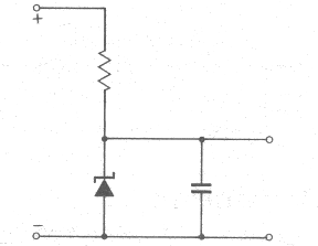
The Basic Circuit
The Basic Voltage
regulator circuit is shown below. It uses only one resistor and one
zener diode. This is called a SHUNT REGULATOR. See SERIES REGULATOR
below.
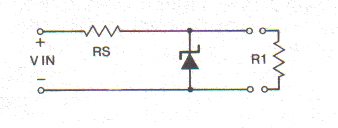
If the Zener diode is rated at 5.6V and the applied voltage is 8.0V,
then with no load applied, the output voltage across R1 will be 5.6V and
the remaining 2.4V will be dropped across Rs, If the input
voltage is changed to 9.0V, then the voltage across the Zener will
remain at 5.6V. In practice, the voltage across the Zener will rise
slightly due to the 'dynamic resistance’ of the zener.
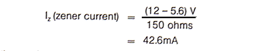
The resistor R1 represents an external load. When this load is connected, some of the current flowing through the zener will now pass through the load. The series resistor Rs is selected so that the minimum current passing through the zener is not less than that required for stable regulation. It is also necessary to ensure that the value of Rs is such that the current flow through the zener cannot exceed its specified power rating. This can be calculated by multiplying the zener voltage by the zener current. The design procedure is as follows:-
1) Specify the maximum and minimum load current, say 0mA and 10mA.
2) Specify the maximum and minimum supply voltages (say 12v) but ensure that the minimum supply voltage is always at least 1.5v higher than the zener voltage being used.
3) In the circuit shown the minimum zener current is 100µA. Thus the maximum zener current (which occurs when there is no load connected) is 10ma plus 100µA equals 10.1mA.
4) The series resistor
must conduct 10.1mA at the lowest input supply voltage, so the minimum
voltage drop across Rs will be 1.5v. Thus the value of Rs
will be:-
1.5v / 10.1X10-3
= 148.5 ohms
This could be changed to
the nearest preferred value of 150 ohms.
5) At the maximum supply voltage (12v) the voltage across Rs
is equal to
the zener current times the series resistor.
This is the maximum (worst case) zener
current. To work out the resulting power dissipation, we multiply this
current by the zener voltage. In this example this works out at:-
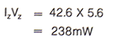
Any zener over this in
power rating would be suitable in this circuit.
Temperature Drift
in Zeners
Typical zener diodes drift in their voltage at about +0.1%/°C at the higher voltages. At lower voltages this goes negative reaching -0.04%/°C at around 3.5v.
This may be made use of in temperature sensing devices. The circuit below shows how a bridge consisting of two similar zener diodes and two resistors can indicate temperature differences when one zener is held at standard temperature and the other is subjected to the conditions to be monitored. If a 10v zener is used, it will have a temperature coefficient of +0.07%/°C giving a change of 7millivolts per degree C.
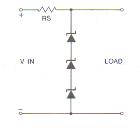
Non Standard Voltages
Non standard voltages can be obtained by connecting zener diodes in series. The diodes need not have the same voltages since this arrangement is self equalizing.
Page 12
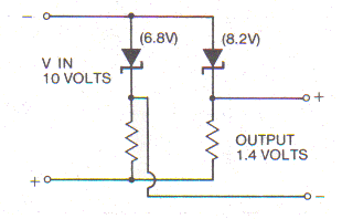 |
It may also be necessary at times to provide a regulated voltage lower than that normally available from a zener diode. These voltages may be obtained by using the difference between two pairs of zeners. This is shown in the circuit below. As a bonus, the temperature compensation of this circuit is excellent, since both zeners tend to drift in the same direction, maintaining the voltage difference. |
Zener Noise
Zener diodes generate noise voltages. These may vary between 10µV and 1mV depending on zener voltage and rating. This noise is easily suppressed by placing a 0.01 to 0.1µF capacitor across it. This reduces the noise voltage by a factor of at least 10.
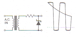
Zener Diode as a Calibration Signal
When supplied with alternating current, the zener diode will limit both the negative and positive halves of the AC cycle. The waveform will be asymmetrical, since the zener will limit almost immediately in one direction, but will not limit until its zener voltage in the other direction.
Increased Power Handling
Although zeners can be paralleled for higher power operation, it is usually a better idea to use a series transistor with a zener reference. This configuration improves the power handling and also the regulation of the circuit by a factor equal to the current gain of the transistor.
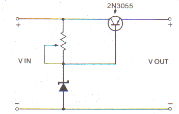 |
The output voltage of this circuit will be equal
to the zener voltage minus the base-emitter voltage of the transistor (approx.
0.7V).
|
Page 13
Constant Current Regulation
This simple circuit maintains a constant current (within approx 10%).
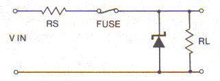
Over-voltage Protection
The circuit below uses the zener as a 'fuseblower'. The zener is selected so that under normal operation it is not conducting. If the circuit develops a fault and the power supply voltage rises above the zener voltage, the zener will come 'on' and draw a heavy current, blowing the fuse.
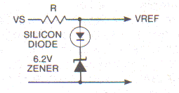
Improving temperature stability
If better temperature stability is required than can be obtained with a single zener, a good trick is to use an ordinary forward biased silicon diode. This makes use of the fact that the forward voltage temperature coefficient of a silicon diode is approximately -2mV/°C. The temperature coefficient of the silicon diode and the zener diode cancel out, giving an almost temperature independent voltage reference. The use of the forward biased diode also allows 'trimming' of zeners to voltages other than the preferred value available. A silicon diode when forward biased will have a voltage drop of 0.7v. When put in series with a zener it will increase the reference by this much. Thus a 6.2v zener plus a silicon diode will give a voltage of 6.9v.
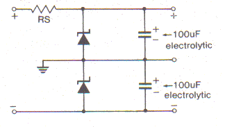
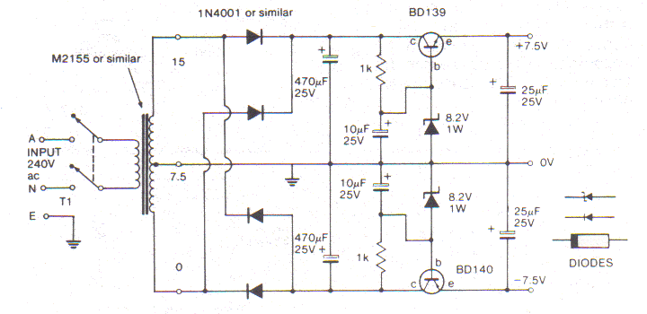
Dual Voltage
Power Supply
The circuit below uses zener diodes to give a split or dual power supply which is ideal for running ICs such as op-amps. The power input only needs to be an unregulated single rail DC source. When selecting Rs it should be remembered that the zener is the sum of the voltage of the two zeners.
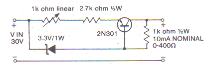
These two circuits show typical use of zeners in power supply circuits. The circuit below is designed to give increased current capacity. It will supply up to 1A with suitable heatsinking of the transistors.
Page 14
These two circuits show typical use of zeners in power supply circuits. The circuit below is designed to give increased current capacity. It will supply up to 1A with suitable heatsinking of the transistors.
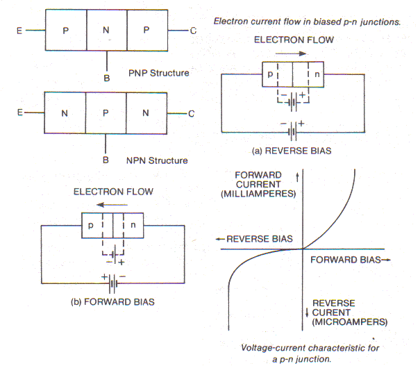
Semiconductor
Devices
The simplest type of
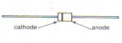
semiconductor device is the diode. It has two electrodes, a cathode and
an anode. II is formed from a junction of P and N type silicon. As shown
below, when the diode is forward biased, by applying a negative voltage
to the cathode (the N type silicon) and a positive voltage to the anode
(the P type silicon) the diode conducts and has a very low resistance.
If the voltage connections are reversed, the diode is said to be
reversed biased and has a very high resistance.
Page 15
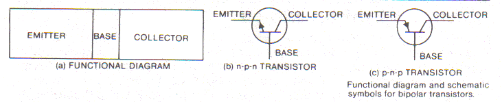
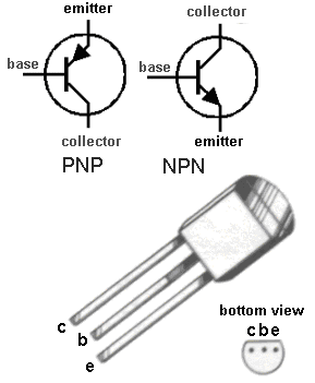
If another layer is added to the semiconductor junction, the resulting
device becomes a bipolar transistor. The three layers of the device are
the emitter, the collector and the base. In normal operation, the
emitter to base junction is forward biased and the collector to base
junction in the reverse direction.
There are two types of transistor, NPN and PNP. The names relate to the 'sandwich' structure of the two types of transistor. They are shown below. For practical purposes, the important difference between the two types of transistor is that in NPN transistors the current flows from emitter to collector. In PNP transistors the electrons flow from collector to emitter.
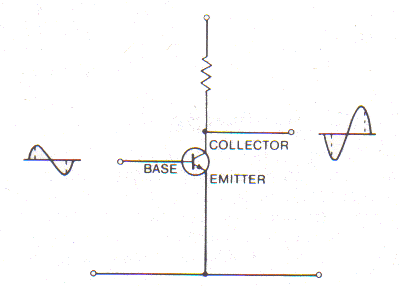
Bipolar Transistors
Bipolar Transistors are current amplifying devices. When a small signal current is applied at the input terminal (the base) of the bipolar transistor, an amplified reproduction of this signal appears at the output terminals (the collector).
There are 3 useful way of
connecting the input signal for amplification.
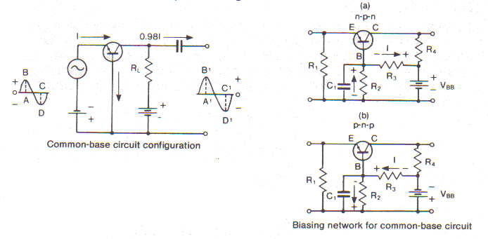
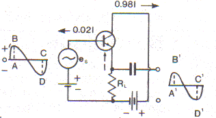
Common Base Mode
In this mode, the signal is introduced into the emitter-base circuit (Thus the base element is common to both the input and output circuits. In this mode, the input impedance is low (i.e. it puts a heavy load on the signal source). The output impedance is fairly high. This type of circuit gives voltage gain and slightly less than unity current gain.
Commonly used as an impedance converter.
Page 16
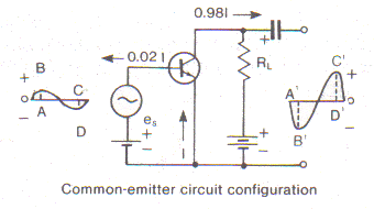
Common Emitter Mode
In this configuration, the signal is introduced into the base-emitter circuit. This arrangement has moderate input and output impedance. It gives both current and voltage gain. Current gain is measured by comparing the base current and the collector current and so is equivalent to HFE A very small change in base current produces a relatively large change in collector current. Depending on the type of transistor this will vary from 5-600.
This is the most commonly used circuit, very often found in audio amplifiers. For an explanation of hfE see definition below.
Common Collector
Mode
In this configuration, the signal is introduced into the base/collector circuit and is 'extracted' from the emitter/collector circuit. The input impedance of this arrangement is high and the output impedance is low. The voltage gain is less than unity while the current gain is high. This configuration is used as an impedance matching device. Commonly called an emitter follower, it is also often used as a current amplifier in power supplies.
Common Collector Mode
Page 17
Darlington Pair
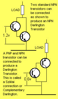 |
The Darlington Pair uses a pair of transistors
coupled together as an emitter follower so that the emitter current of the first
transistor flows through the base/emitter junction of the second transistor. The
resulting current gain of the transistor pair is found by multiplying the
current gain of the transistors together. The resulting current gain is very
high and the input impedance of such a stage is very high.
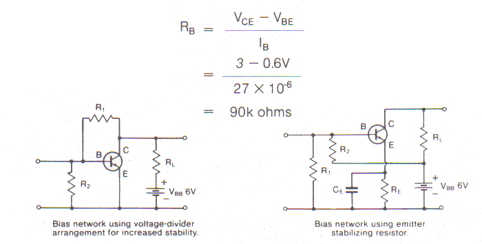
Biasing Arrangements For
linear amplification as opposed to switching applications, the 'operating point'
of the transistor must be set so as to minimize distortion. The simplest of
biasing arrangement is shown below. The base resistor RB is selected
to provide the desired base current, which is 27µA in the example shown. This
base current turns the transistor 'on' and establishes the collector current.
|
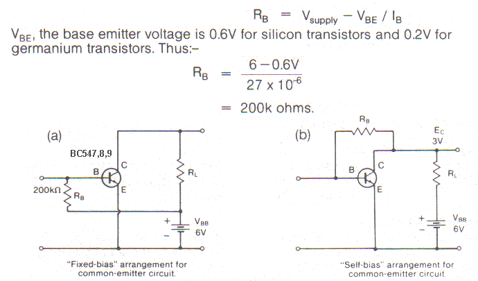
This arrangement is sensitive to temperature and varying gains of transistors. A better arrangement is shown above (b). This stabilizes the operating point of the transistor because an increase in collector current drops the collector voltage and thus decreases the base bias.
Page 18
Definitions
Alpha (a) Gain
In the common base mode,
the emitter is the input electrode and the collector is the output
electrode. The alpha is the ratio of the collector current lc
to the emitter current IE. It is always less than 1.
Beta current gain (hFE)
In the common emitter
mode, the base is the input terminal and the collector is the output
terminal. The beta is the ratio of the collector current lc
to the base current IB.
Gain Bandwidth Product (fhfe)
This is the frequency at which the alpha or beta (according to the type of circuit) drops to 0.707 times its 1 kHz value.
Transition Frequency (fT)
The frequency at which the small-signal forward current transfer ratio (common-emitter) falls to unity.
Breakdown voltage
This defines the voltage between two electrodes at which the current rises rapidly. The breakdown voltage may be specified with the third electrode open, shorted or biased to another electrode.
Secondary Breakdown
High voltages and
currents passing through a transistor cause current to be concentrated
or focused on a very small area of the transistor chip causing localized
overheating. This is important in power transistors which are often
designed to minimize this effect.
Saturation Voltage (Vcesat)
For a given base current, the collector-emitter saturation voltage is the potential across this junction while the transistor is in conduction. A further increase in the bias does not increase the collector current. Saturation voltage is very important in switching and power transistors. It is usually in the order of 0.1v to 1.0v
Safe-operating-area
Power transistors are often required to work at high currents and high voltages simultaneously. This ability is shown in a safe operating area curve.
Ptot
The total package power dissipation
Vcbo
The dc voltage between the collector terminal and the base terminal when the emitter terminal is open-circuited.
vceo
The dc voltage between
the collector terminal and the emitter terminal when the base terminal
is open-circuited.
Page 19
BC547-9 (BC107-9) NPN
BC557-9 (BC557-9) PNP
Low frequency, general purpose
small signal transistors widely used in audio, switching and television
circuits. The BC547-9 series and BC557-9 series are functionally
identical to the common BC107-9 series.
All have a maximum power dissipation of
500mW. They have essentially similar specifications and can generally be
substituted for one another (within the PNP and NPN groups of three
each). All devices are housed in standard TO-92 plastic packages.
|
Specifications |
|
|
|
NPN BC547 |
BC548 |
BC549 |
|
vcbo 50v |
30v |
30v |
|
Vcto 45v |
30v |
30v |
|
lc 100mA |
100mA |
100mA |
|
Ptotl 500mW |
500mW |
500mW |
|
hFE min-max at I0 2mA 110 - 800 |
110 - 800 |
200 - 800 |
|
fT typical 300MHz |
300MHz |
300MHz |
|
VCEsat (max) at lc 100mA/lB 5mA 600mV |
600mV |
600mV |
|
|
|
|
|
PNP BC557 |
BC558 |
BC559 |
|
vcbo 50v |
30v |
30v |
|
vceo 45v |
30v |
30v |
|
lc 100mA |
100mA |
100mA |
|
P,ot 500mW |
500mW |
500mW |
|
hFE min-max at lc 2mA 75 - 475 |
75 - 475 |
125 - 475 |
|
fT typical 150MHz |
150MHz |
150MHz |
|
VCEsat (max) at lc 100mA/lB 5mA 600mV |
600mV |
600mV |
Page 20
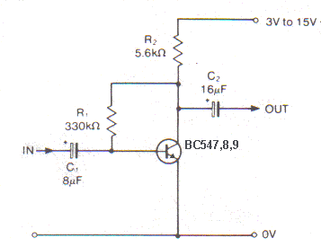
A Simple Amplifier
|
This circuit will operate on any supply from 3v to 15v. Using a 9v supply, the circuit gives a voltage gain of 46dB (200 times), frequency response within 3dB from 30Hz to 100kHz, input impedance of 1.5k ohms and an output impedance of 5.6k ohms. The base bias resistor R1 gives sufficient negative feedback to compensate for the large variation of hFE values in individual transistors and for variations in supply voltage. |
Relay driver
This simple circuit increases the sensitivity of a relay so that it will trigger at 700mV at 40uA. Any relay with an operating current of less than 60mA and operating voltage of less than 12v is suitable. The circuit's supply rail should be at least 3v higher than the operating voltage of the relay.
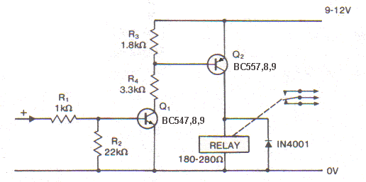
The circuit will work with any relay with a coil resistance higher than 180 ohms and a pull in voltage of less than 12v.
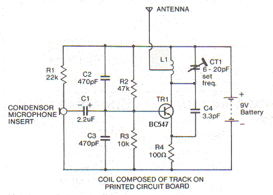
FM transmitter
This circuit, is about as simple as a transmitter can get. The coil is etched onto the printed circuit board, but can be easily substituted by 6 turns on a 4mm diameter former.
Page 21
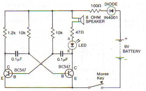
Multivibrator- Morse Code Generator
This circuit is an astable multivibrator or square-wave generator. The circuit is suitable as a morse code generator. The frequency of operation can be raised by making the value of the capacitors smaller. The speaker can be any general purpose 8 ohm type.
BD139/140 Driver
Transistors
BD139/140 are complementary
silicon driver transistors designed for audio and switching
applications. They come in TO-126 plastic cases. The BD139 is an NPN
device and the BD140 is PNP.
Features
• High gain (hFE40-250) • High fT (250MHz for BD139, 75MHz for BD140)
|
Absolute Maximum Ratings
Collector-Emitter Voltage (VCEO)
BD139
80V
BD140
80V
Collector-Base Voltage (VCBS)
BD139
100V
BD140
100V
Collector Current Continuous (Ic)
Total Device Dissipation (Ptot) BD139/140 8W |
Specifications
DC Current gain
(hFF)
@ lc = 150mA
40-250
(BD139/140)
fT(MHz)
BD139
250MHz
@ lc = 500mA
0.5V (BD139/140)
IB = 50mA |

Basic
Amplifier
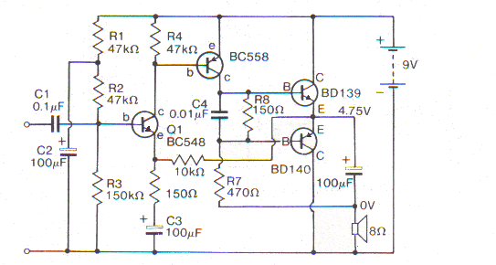
|
The circuit is for a low power amplifier using a
BD139/140 pair in the output stage. The amplifier has a gain of
66. |
This completes Pages 1 to 21 of Data Book 1.
http://www.talkingelectronics.com
Sept 2008 Nothing is copyright. You can copy anything.
Colin Mitchell
to pages: 22 to 41