Logic Probe Mk IIB
Essential for servicing all types of Digital
circuits
email
Colin Mitchell for kit prices
Go to
Talking Electronics website
See also: Super Probe
MkII
![]()
A Logic Probe is one of the most important pieces of test equipment for the
digital designer.
Digital circuits will be covered in this e-magazine and their testing
involves a completely different approach to anything else. They require special
test gear to pick up very fast pulses to let you know if the circuit is
operating correctly.
The most important piece of gear to do this is the Logic Probe. It lets you know if the lines of a particular device are HIGH or LOW or
if a very brief pulse is present.
|
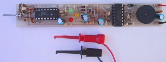
Top view of the Logic Probe Mk IIB |
|
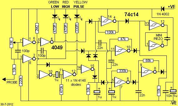
Logic Probe Mk IIB Circuit |
The Logic Probe is the digital technicians equivalent to the audio man's CRO (Cathode Ray Oscilloscope), and is specially designed for the job.
The reason why it is better than a CRO is due to the speed of a digital circuit.
You may be looking for a pulse that is appearing only once every second and its width may be a millionth of a second wide!
It would be very difficult to pick this up on a CRO but a logic probe catches the pulse and displays it on a Pulse LED so you can see it, as well as giving an audible beep from a piezo.
A logic probe is much easier to use than a CRO as it is capable of picking up all types of pulses including glitches and spikes that may be false triggering the project under test.
If you view some of the output lines of a digital circuit with a CRO, you may see "bips and bumps" and the waveforms produced on the screen will be very hard to interpret.
The Logic Probe does all the interpretation for you. It is very easy to use as it has 3 LEDs to indicate the state of the tine while the piezo gives an audible indication when a waveform or pulse is present.
It is designed to respond to only those pulses that digital chips pick up, so you don't have to make any complex decisions.
A digital circuit may have a lot of noise on the lines that run between the chips and unless they are of sufficient amplitude to clock the chips, they will be ignored by both the circuit and the probe.
One point to remember: the tone from the piezo is not the frequency of the pulses on the line. These tones are generated by the probe and don't come from the circuit you are testing.
The tones allow you to keep your eyes on the probe tip while testing each pin of a chip.
It is essential not to allow the probe to slip between two pins of a chip as it may create a short. The tones allow you to keep your eyes on the job and prevent a disaster.
The second most important piece of test gear for digital repairs is a CONTINUITY TESTER. This simple piece of test equipment measures continuity between two points on a circuit and produces a beep.
You could use a multimeter but it is much slower. Sometimes you have to measure between all the pins of a 24 pin chip and this could involve over a 1,000 tests! The continuity tester has been described in this series of test equipment projects
You will also need a multimeter for voltage checks but best of all, you don't need a CR0 for digital work and that will save a lot of money.
HOW THE CIRCUIT WORKS
The probe uses 2 IC's and a handful of components to indicate the state of the input on 3 LEDs while the piezo gives an audible indication of the state of the line.
The input is connected to two inverters in the 4049 IC. The top one is held above mid-rail via the 1M trim pot while the bottom one is held below mid rail by the 1M/220k voltage divider.
The object is to keep those two inverters in a stable state so that they will change state when an input waveform is detected.
The output of the top inverter passes through another stage of inversion so that the result is equivalent to that of a buffer.
The pulse circuit is taken from the lower inverter and passed through a pulse stretcher made up of two inverters in a monostable mode, to illuminate the pulse LED.
The 3 indicator LEDs (HIGH, LOW, PULSE) must not be illuminated when no signal is present. To achieve this, the output of the 3 driving circuits must be high, and go low when the appropriate LED is to be turned ON.
The 1M trim pot on the input line sets the voltage on pin 7 of the top inverter so that the LOW LED is illuminated when the probe detects a LOW.
The inverter between pins 3 and 2 turns on the HIGH LED when the probe detects a HIGH.
The 100p capacitor (between pins 3&7 of the inputs of these two blocks) acts as a speed-up capacitor.
The pulse stretcher is taken from the output of the HIGH inverter via a 100p capacitor and the input of this monostable is high due to the presence of the 2M2 resistor. This makes the output pin 12 low. The 1u electrolytic sits in an uncharged condition and the output is high so that the pulse LED is not illuminated.
The circuit is triggered into operation via the 100p on input pin 9, when output pin 2 goes low. This causes pin 12 to go high and takes pin 14 high with it.
Pin 15 goes low and the latching feature is provided by the diode between pins 12&9. When pin 12 goes low, pin 9 is pulled low and the circuit latches into this state.
The time-delay for the circuit is controlled by the charging of the capacitor, via the 470k resistor.
The voltage on pin 11 gradually falls and at about 40% of rail voltage the inverter changes state and pin 12 goes HIGH. The pulse LED will go out and the low on pin 9 (provided by the diode) will be removed.
The inverter between pins 9&10 will change state and the charge on the 1u will be removed fairly rapidly due to the presence of diodes on the input line (pin 11) of the second inverter.
The remainder of the logic probe is handled by the Schmitt trigger IC.
When a LOW is detected, the low LED turns on and the line also passes to a tone oscillator between pins 3&4 of the 74c14 to produce a low tone. The output of this oscillator is buffered by a pair of inverters to drive a piezo. These fantastic little devices are effectively a crystal that changes shape when a voltage is present between its two electrodes.
By connecting it as shown, it sees a voltage that is double rail voltage and this accounts for its loudness.
When a HIGH is detected, the high tone comes into operation and the piezo is pulsed with a square wave to give the characteristic piezo sound.
The diodes between input and output of the tone circuits are gating diodes to allow pulses from different blocks to feed into the one circuit.
The diode between pins 6&9 turns on the Schmitt oscillator between pins 9&8 when the anode of the diode is low. This allows the 22n to discharge via the 68k resistor and the circuit will start to produce a tone. When the anode is high the 22n remains charged and the oscillator is prevented from operating. This is a simple way of "gating" or turning the oscillator on and off.
The output from the pulse stretcher circuit is taken from an inverter between pins 14 &15 and passed to a pulsed-tone circuit made up of a Schmitt inverter between pins 5 & 6 and 9 & 8. At the same time both high and low tone sections are disabled.
A power diode is provided in the positive rail to prevent damaging the probe with reverse voltage if connected to the power around the wrong way.
The 1u and 10n capacitor across the rails help remove spikes from the power rails and prevent false triggering. The 10k input resistor prevents the circuit being tested, from overload or damage.
|
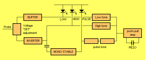
BLOCK DIAGRAM |
|
|
|
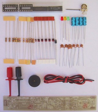
Logic Probe Mk IIB kit |
|
PARTS LIST |
|
1 - 330R all resistors .25watt 2 - 470R 3 - 10k 1 - 47k 1 - 68k 1 - 100k 1 - 220k 1 - 330k 1 - 470k 1 - 2M2 1 - 1M mini trim-pot 2 - 100p ceramic 1 - 10n ceramic 3 - 22n ceramic 4 - 1u 16v PC mount electrolytics 11 - 1N 4148 signal diodes 1 - 1N 4002 power diode 1 - 4049 hex inverter lC 1 - 74c14 or 40106 hex Schmitt IC 1 - 3mm red LED 1 - 3mm yellow LED 1 - 3mm green LED 1 - mini piezo 1 - 14 pin IC socket 1 - 16pin IC socket 1 - red EZ clip 1 - black EZ clip 40cm red hook-up wire 40cm black hook-up wire 1 - nail for probe 1 - LOGIC PROBE PC board (Buy a soft toothbrush case from the chemist to house the probe) |
|
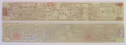
Logic Probe Mk IIB PCB |
CONSTRUCTION
Before starting construction, the first item you must organize is the case.
The best type is made of soft plastic as it will withstand knocks and scratches
without cracking.
It is made by a process called vacuum forming and is similar in appearance to
plastic drinking cups and you know how strong they are.
Once you have the case you can lay the kit of components on the bench and
identify all the values. Fit the board into the case so that you can see how
much headroom you have. This is why all the parts must be fitted close to the
board and some need to be pushed over slightly to allow the board to slide into
the case.
All the parts supplied in the kit are the right size and if you are buying
parts separately, you must check to see that they are small enough.
The first two items to be fined are the two IC sockets. A small identification
mark is located at the end of each socket and this fits over pin 1 so that when
the IC's are to be fitted, you know which way they go.
Next fit the resistors. The overlay on the board and the photos will show that
some of the resistors stand up while others lay down. Keep them close to the board when soldering and make sure the board will still slip into the case.
The signal diodes and power diode are next. If you keep one finger on or near
the diode when soldering you will not get it too hot and if you solder very
quickly there will be no chance of damaging anything. The line on the diode
represents the cathode end and this is shown on the board by a diode symbol.
The electrolytics are next and these must be placed around the correct way for
them to function correctly. The positive hole is marked on the board and this
corresponds to the long lead of the electro.
The small capacitors are next and can be fitted either way around.
The three LEDs are the most delicate components as they will lose their
brightness if heated up too much. Don't spread the leads apart as this will
damage them but fit them down the correct holes so that the short load goes
down the hole identified with a line on the overlay. Make sure the top of the
LED is low enough for the board to slip into the case. Solder quickly and
cleanly.
The probe tip is made from a paper clip. This is very hard springy steel so
don't try to cut it with pliers as the steel will damage the cutters. Use a hack
saw or file or bend it sharply a couple of times and it will fracture. Bend it
back on itself to form a "U" shape to make the joint stronger and solder it to
the board.
The power leads for the probe should be as tong as possible as you need plenty
of length when you are moving the probe around a project such as tracing a
fault on the top and bottom of a board.
The last two items to be soldered are the alligator clips. The leads have to be
fitted through two holes in the end of the case and then the clips can be
connected.
Fit the two IC's so that pin I covers the dot on the overlay. This is most important as they will be damaged it fitted
around the wrong way. Before the board is slipped into the case, connect the
leads to a 9-12v supply and touch the tip to the negative terminal of the
supply. Adjust the mini trim pot until the LOW LED is just illuminated. The
probe is now ready. Slip it into the case and tape the two halves of the case
together.
IF IT DOESN'T WORK
If none of the LEDs come on when the probe is connected to the positive or
negative rails, the most likely cause is a faulty 4049 or the LEDs have been
fitted around the wrong way.
Remove the 4049 and connect the power leads of the probe to a 9-12v source.
Take a jumper lead and short between pin 4 of the 4049 and ground. The green
LED should come on. If not, the LED has been filled incorrectly or damaged
during soldering.
Replace it and try again. Short between pin 2 and negative for the red LED to
come on and pin 12 and ground for the yellow LED.
Once you know they all work, the IC can be put back and the probe tested again.
If the pulse LED doesn't work when the probe is taken to the positive Line,
take a lumper from pin 11 to the positive rail and it should illuminate. If
not, something is preventing pin 12 from going low. It could be the inverter
between pins 11 & 12 or a fault in the track-work or even a short across the
2M2, keeping pin 9 & 12 high.
Take a jumper from pin 9 to negative. If this
doesn't turn on the pulse LED for a short period of time, the fault may lie in
the 1u between pins 10 & 11 not working or not connected to the board. Try
shorting between pins 10 & 11 with one jumper lead and take pin 11 low again
with another lead.
The only other component affecting the pulse line is a 100p capacitor. Try
shorting across it and take the probe tip high.
The 3 tones are produced
separately and if no tone is emitted, remove the two diodes on pin 3 of the
74c14 and the low tone should be produced.
If not, the Schmitt trigger between pins 3 & 4 is faulty or the 22n or 100k are
not fitted correctly.
If still no tone, remove the diode on pin 10 and on pin 8. To test the
inverters between pins 13 & 12 and 1 & 2, connect a piezo between pin 4 and
negative rail. This will prove the oscillator between pins 3 & 4 is
functioning.
Short between pins 4 & 13 to prove the diode has been fitted correctly and the piezo should be working by now.
If the high tone is not produced, the inverter between 11 & 10 will be faulty
or the 22n, 47k will be at fault.
You can also remove the two diodes on pin 11 to produce the high tone and if it
is still not being produced, you can connect a piezo between pin 10 and
negative rail to detect the tone.
The pulse frequency is a little more complex however we know the piezo drivers
are working so removing the diode between pins 6 & 9 will produce a constant
tone. If not, the oscillator between pins 9 & 8 will be faulty or the 22n, 68k
or gating diode on pin 8 will be the fault.
Once the middle tone is produced, replace the diode between pins 6 & 9 and
remove the diode on pin 5. This will give a pulsed tone and if not, the low
frequency oscillator between pins 5 & 6 will be faulty or the 1u or the 330k on
pin 5.
Your probe should be working by now. Make sure all the components are soldered
back on the board and it is ready to give years of useful service.
USING THE PROBE
The power for the probe is obtained from the project you are testing. This way
the voltage is automatically adjusted to match the project.
Connect the positive lead to any positive rail on the project you wish to test
and the black lead to ground.
Start by using the probe on a known project so that you can identify the
HIGH/LOW tones. Always refer to a circuit diagram when checking a circuit and
ask yourself "Will it be HIGH, LOW or give a PULSE?" before using the probe.
The tones will confirm your reasoning and show what is occurring.
You will find this project essential for digital work and equal to anything on
the market.
![]()