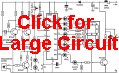
PIC LAB-1
P1 - lower half
THE PIC LAB-1
The PIC LAB-1 printed circuit board can be divided into three sections:
1: Amplifying (or interfacing) circuitry for the input devices,
2:
The microcontroller, and
3: Output devices.
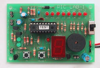
Top view of PIC LAB-1
The top socket (Pot) is the A-to-D conversion input, the middle socket (mic/coil) is the analogue input and the Probe socket detects temperature.
THE OVERLAY
The overlay for the board clearly shows where each component is placed. The
advantage of buying a kit is each component is designed to fit the board.
Click the "Buy Kit" button on the left-hand side of the page and the
kit will be sent the same day. All boards have a screened top layer showing
the position of the components and the underside is solder-masked so that only
the lands are exposed and tinned without any blocked holes. Four corner mounting
holes allow the board to be fixed to the top surface of a box or lid for
demonstration purposes or class project etc.
INPUT DEVICES
Using a PC board prevents a wiring mistake and assembling a kit means you have
the highest chance of success. The kit comes with a pre-programmed chip
with a Test Routine and a section on "If it Doesn't Work" is
included below, to help with any problems that may arise.
The 10mH choke (coil) must be wound on the ferrite former,
using the .005" (5 thou) wire provided. The number of turns is not important,
however it is best to wind as many turns as possible on the former until the
winding is flush with the outer edge. This will produce a coil with about 300
turns and it will have a resistance of about 15 ohms. The resistance is not
important, however each turn will increase the voltage generated when a magnet
is passed across the end of the former.
TEST ROUTINE THE INPUT TEMPERATURE PROBE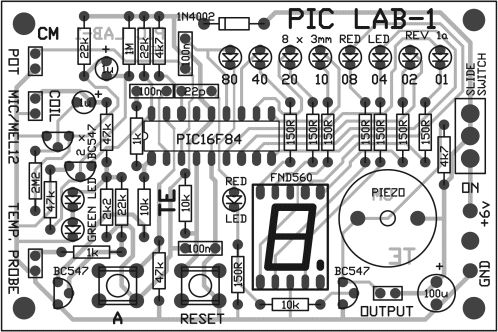
Many input devices cannot be connected directly to a microcontroller. They either produce a very small
AC voltage or a change in resistance. These devices must be connected via an
amplifier.
The amplifier increases the amplitude of the signal to a DIGITAL LEVEL. In the
case of a change in resistance, the device is connected to the supply rail via a
resistor and the change in voltage across the resistor (you can also say
"the change in voltage across the device") is amplified (via a
transistor) and passed to
the microcontroller. If the device produces a voltage or resistance
that changes over a long period of time, other interfacing circuitry must be
used. This will also be covered in the project.
It is the job of the program to detect a signal from the device and process it correctly. In
our case this involves turning on LEDs, showing the result on a 7-segment
display and/or producing a tone from a piezo
diaphragm.
THE MICROCONTROLLER
The PIC16F84 microcontroller has 13 lines that can be programmed as inputs
or outputs ( in ANY combination).
It has a code-protection feature, so
the program cannot be "looked at" by any outsider and thus any project
you design can be protected.
The microcontroller we are using may be considered very simple and limited when compared to some of the
larger microcontrollers, but its capability will certainly allow quite
impressive projects to be developed. And most-importantly, it allows you to
start at the beginning.
One of the aims of this course is to steer you into programming and designing.
For this, we need to start at square-one, and talk about complexities, later.
OUTPUT DEVICES
The output devices on PIC LAB-1 consist of a set of 8 LEDs and a 7-segment display, as well
as a piezo diaphragm. A buffer transistor allows a relay, globe, motor or speaker to be connected.
This gives a large number of combinations for outputting the data.
Before we go any further, you will need two other things:
A PIC16F84 chip and a Programmer to program the chip.
Talking Electronics has produced a Multi-Chip Programmer
suitable for programming the PIC16F84. It can be assembled in less than an hour and comes with a serial
cable (in kit form) to connect to the serial port of your computer. The PIC16F84
chip comes with the PIC LAB-1 kit. It can be re-programmed about
1,000 times.
With a Programmer, Chip and PIC LAB-1 you have the equipment needed to study the
concepts of writing PIC programs and developing quite complex
projects.
Many projects presented in books and magazines, using ordinary logic chips and
discrete components, can be converted to a
PIC design and the "building blocks" on PIC LAB-1
will help create a micro controlled project.
This will be the discussion for an article in the future (we have already
produced other modules using this chip). For the moment we need
to explain how to create some of the simplest routines.
But the first thing to do is assemble PIC LAB-1. This has been made easy with
a fully-detailed printed circuit board. All the components are clearly
identified and the kit contains the smallest, neatest, components available. The supplier of the kit
is TALKING ELECTRONICS. The cost is less than
if the components were bought separately and we suggest you invest in a kit.
To order, simply click the button.
You can buy the kit or a "Ready Built and tested" version.
![]()
![]()
The board has been designed for both functionality and presentation. It should
NOT be housed in a box as you need to access the buttons and IC. The chip is
transferred to and from the Multi Chip Programmer in a "carrier." This is an 18 pin IC socket fitted to the base of the chip. The two are moved
as a "unit." This makes the chip easy to insert and remove from the socket
on the PC board and prevents the pins stabbing your
fingers.
Simply move the chip sideways and it will come out of the socket. You don't
need an expensive ZIF socket!
The PIC chip in the kit contains a special TEST ROUTINE to test
each of the input and output devices.
Once the kit is assembled, insert the chip and switch ON. Go to the
Test Routine section for further details.
The project is now ready.
The site contains over 25 programs, including the HEX listing for
the Multi-Chip Programmer and this will provide you with the basics to produce
routines for your own projects and ideas.
CONSTRUCTION
Construction is made very easy by referring to the overlay on the PC board. It shows exactly where
each component is placed and its
orientation. Fine solder
is included in the kit to make the overall appearance of each joint very
clean. Fine solder makes an enormous difference to the quality of the joint and you need a
low-wattage iron for the delicate work. Low-wattage does not mean
low-temperature (at the tip) and if the solder smokes as soon as you apply it, the
iron is too hot.
A power-diode in series with one lead will reduce the temperature
to the correct value. Get a qualified person to add the diode for you - he
will understand its function.
Clean the tip of the iron with fresh solder before starting a connection (if
the iron has been left standing for any length of time) and tap off any
excess. Add more solder when the iron is actually heating the
component-lead. Make sure the joint is bright and shiny after completion, before going to the
next connection. Do not touch or wiggle the joint until it has thoroughly
cooled down.
Only add one or two components to the board at a time and snip the leads after
each operation. These are the basics you MUST adhere to.
There are many ways to fill the board. You can start with the high components,
such as the IC sockets and then the small components, or move across the board from
left-to-right, fitting each component as you come to it. The best way is to
add the IC socket first, to fill the majority of holes. The
most important point is to hold the component in your fingers while soldering and if it gets
too hot to hold, you are taking too long. The author always holds each component
to make sure nothing is damaged by overheating.
Push the components up to board before soldering, except the transistors
and LEDs. These should be 1/4" (3mm) from the board to prevent heat
running up the leads and damaging the semiconductor material inside.
The 7-segment display is identified by the decimal point at the base of the
display.
The final item to fit is the battery snap.
Fit the pre-programmed PIC chip and the project is ready for testing.
The input devices such as the microphone, coil, photo-transistor and
potentiometer, are connected to the board via small 2-pin plugs. These fit
into sockets made from
machine-pins. 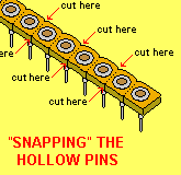 These plugs and sockets are cut from a strip by scoring between the pins with
a sharp knife and breaking with your fingers. The
microphone and darlington photo-transistor must be plugged-in around the correct
way and if they are soldered to the plug and bent as shown in the photos, they
cannot be plugged-in around the wrong way. They will not be damaged if reversed,
however it is best to make sure they are connected correctly. They can be
connected via a short lead if required.
These plugs and sockets are cut from a strip by scoring between the pins with
a sharp knife and breaking with your fingers. The
microphone and darlington photo-transistor must be plugged-in around the correct
way and if they are soldered to the plug and bent as shown in the photos, they
cannot be plugged-in around the wrong way. They will not be damaged if reversed,
however it is best to make sure they are connected correctly. They can be
connected via a short lead if required.
The potentiometer and diode are also connected to the board via a 2-pin
plug.
 By bending the microphone, diode and
photo-transistor to 90°, the plug is effectively 'polarised,' it can only be
fitted around one way.
By bending the microphone, diode and
photo-transistor to 90°, the plug is effectively 'polarised,' it can only be
fitted around one way.
CONNECTING THE INPUT
DEVICES
The input devices are soldered to machine pins that fit into a machine socket
on the PC board. The orientation of some input devices is important as they
will not work when connected around the wrong way. The diagram below shows how
to connect each item: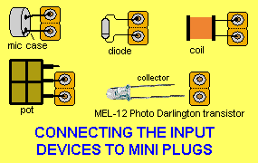
Fit the sleeve over the winding and shrink with a hot flame such as a match or
cigarette lighter.
Clean the ends of the fine wire with a blade and solder to the ends of the
thick wires where they emerge from the former. Bend one lead over to produce a
one-ended inductor. Cut both leads to the same length and solder them to the
machine pins provided, to produce a plug.
PIC LAB-1 kit comes
with a pre-programmed chip containing the TEST ROUTINE. Turn the project ON and the row of 8 LEDs will scan across and back. The
individual segments of the 7-segment display will also turn ON. Push
button "A."
The letters "Pb" will show on the 7-segment display - for "Push
button."
Push button "A" again and the top 4 LEDs will blink, followed by the lower 4
LEDs. Push button "A" again. The letters "AUdiO" will
show on the display. Push button "A" again.
Fit a microphone to the 2-pin plug marked "MIC" and talk or whistle.
The lowest LED will turn ON to indicate
audio. Push button "A" again.
The letters POt will flash on the 7-segment display. Push button
"A" again.
Insert a potentiometer into the 2-pin plug labelled "Pot" and rotate it in both directions. The
7-segment display will indicate rotation.
All the input and output devices are now tested.
Push button "A" to repeat the sequence.
IF IT DOESN'T WORK
If the project doesn't
work, there are 4 areas to investigate.
They are:
The INPUT, the MICROPROCESSOR, the OUTPUT, the PROGRAM.
These notes apply to a project that has assembled from a kit with the pre-programmed PIC chip
fitted to the board. Anything built on matrix board, using junk-box parts, may
have any number of other introduced faults. 99% of faults eventually boil down
to the builder using non-kit components and failing to let us know. After
dozens of emails we finally realise he has used "odd-ball"
components.
A capacitor may appear to be "22" but is really
"2.2" A resistor may appear to be 100k, but is really a 1% type
and the colours have been read incorrectly.
Here is a resistor colour-code calculator for
1% types
and 5% types.
If the operation of pushing the switch does not work in the TEST ROUTINE, It may be faulty, fitted to
the board incorrectly or not soldered. The 47k resistor may be missing or not
soldered. Measure pin 17 of the chip and make sure it goes HIGH when the
switch is pressed.
The TEST ROUTINE may not be responding to the switch. You can try Experiment
1, if you think the Test Routine is faulty.
THE MICRO
If the 8 LEDs do not illuminate, you will need to test pin 14 for approx
5.4v Also check pin 16 for approx 5.4v (clock in).
The most likely fault is the chip failing to "clock." Check the 22p.
The chip has been pre-programmed and checked in a PIC LAB-1 project, before it
is sent with the kit, so it
will NOT be faulty.
The main problem will be the 22p and the impedance of the circuit. At 4MHz the
chip is operating at its maximum frequency and if the circuit is not
"tight" the chip will fail to oscillate. The answer is to reduce the
frequency at which the chip will be oscillation, by adding a 22p to 100p
across the 22p. You should also make sure the batteries are fresh.
To reduce the impedance of the circuit you can add another 100n across the
rails NEAR the chip.
You can also check for shorts and dry joints around the chip as well as
incorrect component values, especially the 4k7 and 22p on the oscillator input
to the chip.
Do not operate the project from a power supply or use long leads to the
batteries. These tend to increase the impedance of the supply and can result
in the chip not oscillating.
Any project built on a "home-brew" board or matrix board can suffer
from a very "loose" supply rail called a high-impedance rail. This
will prevent the chip oscillating.
It's a bit like getting 4 people to hold a trampoline in the air while you
bounce on it. You can see exactly what would happen. You would not be able to
get any spring into the air.
The same happens with the internal oscillator of the chip. If the supply rails
are loose, the chip fails to oscillate.
THE OUTPUT
If some LEDs do not illuminate, they may be around the wrong way. If the
display is up-side-down, only the end LED will illuminate. If the LEDs are
damaged by excess heat during soldering, the output will be very weak.
THE PROGRAM
If a program from one of the experiments does not work, you will have to go
over all the steps involved in producing the program.
The hardware side of the project is operational as it has been tested via the
TEST ROUTINE.
If this is the first program you have "burnt" into the chip, you
will need to check the Multi Chip Programmer project and the serial
cable.
You can read and verify the program in the chip via the Multi Chip Programmer to see if it has been loaded
correctly.
Also check the config settings. These are also called "fuses"
and will also prevent the chip operating if not set correctly. If the chip is
set to operate with a Xtal, it will not
"clock" with RC components. In the top right-hand-side window,
make sure RC is showing in the window.
For the experiments in this project, the fuse settings (WDT, PWRT and CP)
must be turned off (unclicked) in IC-Prog.
HOW THE CIRCUIT WORKS
The circuit consists of
three sections. The input device and its associated amplifying circuitry, the
microcontroller and the output device.
One or more input devices can be connected to the circuit at the same time and
the program (in the microcontroller) detects the presence of the device and
produce an output to activate one or more display devices.
The main purpose of the input-amplifier is to increase the amplitude of a
signal to a level called DIGITAL LEVEL. This is an amplitude of at least 75% of
rail voltage and a minimum of about 10%. This is needed to make sure the micro
detects a HIGH and LOW.
A waveform below Digital Level is called an ANALOGUE waveform and the
amplifier that converts (amplifies) the signal is called an Analogue-to-Digital stage, or A-to-D amplifier. It is
given this reference-name to show the stage must have sufficient
amplification to produce a digital signal.
We have provided sufficient gain for all the devices in the experiments with a two-stage amplifier and the actual term is
OVER-AMPLIFICATION. This is to ensure the signal is at a digital level. The
first stage is a self-biased common emitter stage with a gain of about 70. It
feeds a second stage and this is where the clever design is evident. This
stage is biased OFF, with approx 500mV on the base. It only needs approx 250mV
signal through the 100n capacitor to turn it on. The collector
voltage will change from rail voltage to about 300mV. The result is a
fairly clean square wave for the
input of the microcontroller.
More details on designing A-to-D amplifiers is provided on other pages in
our site.
The circuitry for the temperature probe is a little more complex. The probe is
a diode and the voltage across it changes by -2mV per degree centigrade. This
means the voltage across it reduces as the temperature increases. This is not
a problem as the circuit and program can be adjusted for any situation. This
is a fairly small voltage change and we have opted to amplify the change by
using a transistor to detect the voltage across the diode.
To turn the transistor ON, a voltage divider made up of a 22k and 1k has been
added in series with the diode. Any variation in supply voltage will alter the
amplification of the transistor considerably and so a constant supply voltage
has been obtained by using the constant-voltage characteristics of two green
LEDs in series. This provides a supply rail of 2.1v + 2.1v = 4.2v for
the base of the transistor.
As the temperature of the diode changes, the voltage on the base of the
transistor alters and this modifies the effective resistance between the
collector-emitter terminals of the transistor.
The micro charges a 100n capacitor via a 1k, 10k and collector-emitter
resistance. As the capacitor charges, the voltage on Pin1 reduces.
The micro detects the time for the voltage to fall to the lower threshold
voltage of an input line and this time is referenced to a table to determine
the temperature detected by the probe.
RESISTANCE
Resistance is measured by a series RC circuit called a TIME DELAY
circuit.
The time taken for a capacitor to charge is detected by the micro and can be referenced
to a table to determine the value of resistance in the circuit.
OUTPUT DEVICES
The output devices are connected to the output port and the program can be
designed to give a reading on the row of 8 LEDs, the 7-segment display or
drive the output transistor to operate a piezo diaphragm, or other device
connected to the output terminals.
THE RESET CIRCUIT
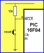 To reset the program in the
PIC chip, the reset button is pressed momentarily. The program will then start
at location "000"
To reset the program in the
PIC chip, the reset button is pressed momentarily. The program will then start
at location "000"
For the reset to work, the program must have instructions in SetUp to clear
(zero) files and turn off any outputs. Files are not emptied by the action of
Reset and it will appear that "reset" is not working if the files are
not emptied in SetUp.
File 06 must be cleared or loaded with a starting value so that the program
appears to be reset when the button is pressed.
THE CIRCUIT:
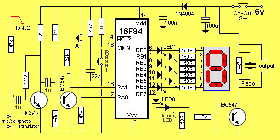
Inputs detected: push-switch, microphone, piezo, coil and photo-transistor
Note the modification above to make the microphone input less sensitive to noise.
Take the 47k microphone dropper-resistor to the 4v2 provided by the two green LEDs.
Inputs detected: temperature via diode, resistance via potentiometer
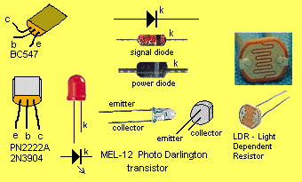
The pin-outs for some of the devices used in this project
PARTS LIST
Kits
for this project are available from Talking Electronics.
| |
|
THE EXPERIMENTS
There are more than 25
experiments for the PIC LAB-1 and the project must be
working correctly before they can be loaded.
Don't forget to test the project with the TEST ROUTINE
(in the PIC chip that comes with the kit) before starting the experiments.
Each
experiment (in a group) starts with the simplest for a particular device and
gradually increases in complexity. They start on the next page and you can see
the list of experiments above. But first you have to know how to burn a
program into a PIC chip.
BURNING A PROGRAM
Each experiment on the pages that follow is shown in a layout very similar to a text-editor. But
it cannot be copied and loaded into a program for burning into a PIC chip as
it contains hidden formatting.
To burn the experiments into a PIC chip, the files have
been zipped for downloading.
The extension you need for the burning process is .hex and these files can be found by
clicking:
PIC LAB-1 Expmts-hex.
You can also see:
PIC LAB-1 Expmts-all
Go to the menu of your computer and create a new folder: PIC
LAB-1
Download the .zip file(s) into PIC LAB-1 folder.
You will also need a programmer to "burn" the PIC chip.
We say "burn" to identify the operation of putting a program into
the chip, rather than "program the chip" as we use
"program" in the context of writing a program.
The PIC Programmer designed by Talking Electronics is Multi
Chip Programmer.
Build the Programmer, test it and have it ready.
You will also need the software to transfer the information from a .hex file
to the programmer.
The software is: ICPROG.
Download
IC-Prog.exe and a help file:
ICPROG-Help (IC-Prog.chm)
Extract all the files into PIC
LAB-1
folder. Place ICPROG.exe into your desktop folder and it will
appear on your screen.
Go you your front-screen (desktop) and open ICPROG.
On the window showing the types of chips the programmer is able to program,
select PIC 16F84.
In the oscillator window, select RC.
In the fuses windows, remove all the ticks.
Click the "open file" icon on the left hand side of the screen.
Find Expt1.hex and load it into the programmer. A tick will appear in the WDT
window to indicate a file has been loaded. Remove the tick.
Make sure the Multi Chip Programmer has been fitted to "Com1" via
a serial cable and the red LED on the Multi Chip Programmer is active.
Click on the IC Icon with the "lightening" and a dialog box with
"Do you really want the program the device?" will appear. Click
"yes" and the orange and green LEDs will illuminate and the screen will indicate the
chip has been programmed correctly.
Remove the chip and fit it to the PIC LAB-1 project. Fit any necessary
input devices and switch ON. The LEDs on the output will respond.
If every thing has gone successfully, you will have "burnt" your
first routine.
Read the instructions for each experiment carefully and follow them to see exactly
how the program is constructed and executed.
As soon as you get to the stage of writing your own programs, send them in
and we will add them to the Readers Experiments Section.