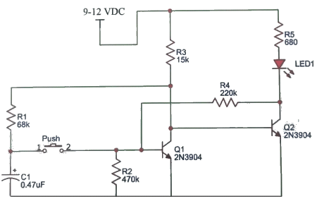
It has a number of faults and will not work at all.
The circuit is far too complex but looking at the base of T1, it will be at 0v
when T2 is turned ON via the delay on its base.
The emitter is connected to the base of T5 and the emitter of T5 we will assume
to be at 12v for the moment.
This means the base of T5 will be 12v and the emitter of T1 will be 12v.
This places the base-emitter of T1 in a reverse voltage situation between the
base and emitter and this voltage can on be about 5v before the transistor
starts to leak. This means the reverse voltage on the base-emitter of T1 will
zener at 5v and the emitter of T1 will not go lower than 5v. Pin2 of the 555
needs to go below 4v for the 555 to start timing and must go above 8v for the
chip to stop timing.
The circuit is such a mess that I don't know what will happen.
The second problem is the 1,000u on pin7 of the 555. Getting pin7 to discharge
this capacitor will put a very high current through the discharge transistor and
damage it.
The third problem is the output of the opto-coupler being able to turn off the
BC558. The load on the output of the coupler is 12mA and I don't know the
voltage across the output with this current. It may not be able to go as low at
0.5v The reason is this: As you load the output of the transistor
device, the transistor cannot fully saturate and the voltage between the
collector and emitter will rise from 0.3v to 0.4v or 0.5v or even 0.6v
It depends of the quality of the transistor and the current is designed to
handle. When you are relying on unusual features like this for a circuit to
work, you have to test a number of devices to see if the whole batch will work
as required,.
The fourth problem is the 7 minute timing. Delays above 3 minutes are very
unreliable with high value electrolytics and high resistances. You are
charging the 1,000u at less than 3uA and the leakage current for this type of
electro can be 3uA so it will never charge. This circuit was designed to go into
an air conditioner for a life of 20 years and and you can see the problems that
will start to show after 12 months and the company will go bankrupt.
The second relay and opto coupler are not needed.
And improved design will eliminate most of the components.
It can be designed much simpler.

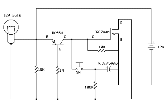
BATTERY VOLTAGE
Here is another circuit from D.Mohankumar.
https://dmohankumar.wordpress.com/
None of his circuits work and he has 2 million Indians going to his
website each month and seeing faulty circuits that don't work and never
will work. It is no wonder the poor Indians are hopeless at
understanding electronics when they see this RUBBISH.
He says: Here is a simple 3.7 volt Lithium-Ion battery level indicator. Green LED
lights when the battery is full with 3.7 to 4.2 volts. When the battery
voltage decreases below 3 volts, Green LED turns off and Red LED lights.
Just connect it to the 3.7 volt battery charger.
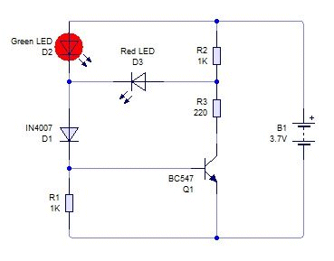
There is no current-limiting
resistor for the green LED. Imagine what would happen to the green LED when the
battery reaches 4.2v. A green LED drop 2.4v The diode drops
0.7v and the base-emitter junction drops 0.7v That is 3.8v A fully charged
cell is 4.2v and after testing the circuit for 1 minute the green LED burnt out.
It got so hot on the high voltage that the crystal overheated and died. I
connected another green LED and the battery voltage dropped enough so the LED did not
burn out. The circuit is badly designed and I suggest you do not build it.
However the red LED did come on at 3v - - so just the green LED section has to
be fixed.
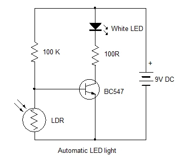
AUTOMATIC LED LIGHT
Another failure from D.Mohankumar.
https://dmohankumar.wordpress.com/
Basically the circuit will not work because the 100R resistor will allow 60mA to
flow and produce good brightness.
The way the transistor works is this: It effectively reduces the 100k by a
factor of 100 due to the gain of the transistor and this means it adds a 1k
resistance to the 100R and less than 6mA will flow. The brightness will be a lot
less than expected and you will wonder why. You have to design a circuit so that
it works 100% better than expected to take into account all the differences in
the features of the components.
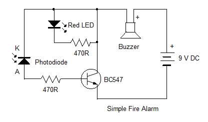
SIMPLE FIRE ALARM
Another failure from D.Mohankumar.
https://dmohankumar.wordpress.com/
The circuit will not work because the LED and resistor will not get any voltage.
A photo diode has a very high resistance and putting 470R in series has no
technical understanding. Turning on a mechanical buzzer slowly like this does
not work. Just try it yourself and see how the circuit fails. Another
untried circuit from Professor Mohankumar who has NO understanding of
electronics.
240V LED
Here is a simple circuit that not been understood by any of the readers or
authors:
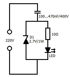
The zener is designed to limit the current when the switch is turned ON
and the mains voltage is at a peak. In this condition the current will be very
high and we know a LED can be destroyed INSTANTLY.
Let me say the circuit is badly designed because it is too close to
destroying the LED when the conditions are such that the capacitor is uncharged
and the switch is turned ON when the supply is at a peak. The current through
the LED at this peak will be 90mA when the characteristic voltage of the red LED
is 1.8v and the zener is 2.7v This leaves 0.9v for the voltage across the 10R
resistor. This will allow 90mA to flow.
A much better arrangement is to use a 100R resistor and the 4mA will flow
normally and when a peak occurs the current will be 10mA.
This is a much better design.
The secret is understanding the resistor can be increased considerably without
affecting the current.
ZENER REGULATOR
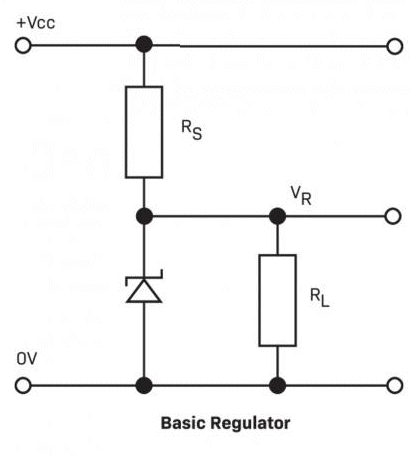
Here is a zener regulator circuit.
The first thing you have to accept is this: The voltage
across the zener will be constant when the current taken by the load changes.
Of course the voltage will change, but if you don't accept the variation, don't
use a zener regulator.
The voltage will change because the zener gets hotter when it is passing more
current and you need to provide good heatsinking.
But if you don't accept CONSTANT ZENER VOLTAGE don't argue with the following
description.
To start with, all zener diodes have a tolerance of +-5% so a 9v1 may be 500mV
less or 500mV more. This means the voltage has a range of 1v !!
That is called the initial setting of the output of the zener regulator. But
when the circuit is in operation, the output voltage will change by only a few
millivolts or maybe 100mV
On top of this, every 9v1 zener will produce a different characteristic voltage
across it when taking 20mA so this is a start to understanding the wide range of
output voltages from a batch of 9v1 zeners.
Suppose you set up a circuit with 20mA flowing through the zener. As you put a
load across the zener, the current flowing through the load will be taken from
the zener-current. The current through the supply resistor WILL NOT
CHANGE. It will simply be split into two paths.
You can keep "robbing" the current from the zener until only about 2mA flows
through it and the output voltage will remain constant.
If you did the same thing with a VOLTAGE DIVIDER made up of two resistors, the
output voltage will drop 2, 3 or 4 volts. The zener circuit may drop 100mV or
200mV. It has much better features. A zener regulator will be
about 50 times better than a voltage-divider. For instance a voltage divider may
change 100mV and a zener circuit will only change 2mV.
In reality the zener will go colder when the load increases and the natural
characteristic voltage across it will alter and drop slightly. That will be main
contributing factor to the change in output voltage. Good heatsinking will
reduce this.
Before we leave this topic, here is a diagram from DIYODE magazine:
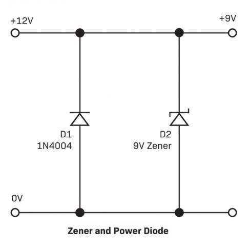
How can one end of a supply rail be 12v and the other end 9v
???? It is blatant, GLARING MISTAKES, like this that are not
corrected and the editor is saying I am: "nit-picking."
If I was a beginner, I would think it is possible to achieve the result above
AND HOW MISLED I WOULD BE.
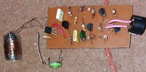
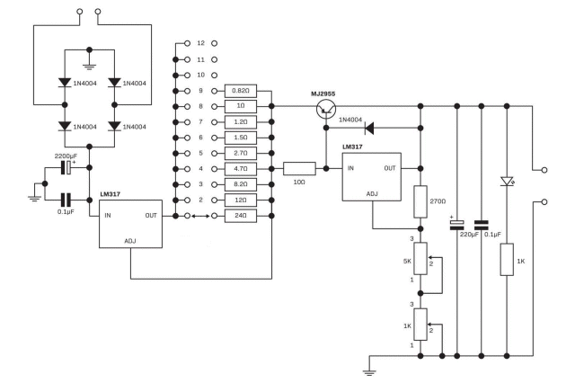
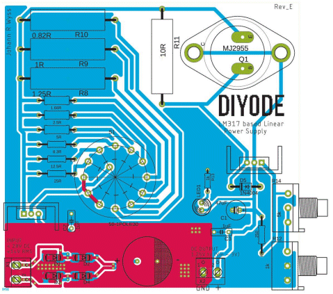
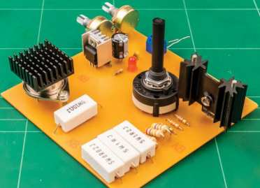
SERIES REGULATOR
Here is a circuit from April 2021 of DIYODE Magazine.
The author is trying to explain how to design a SERIES REGULATOR circuit.
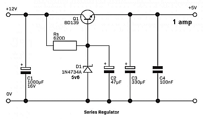
But he is missing the hidden
facts and disasters of using a transistor such as a BD139. He does not
understand the BASICS of electronics and that's why he has made so many
mistakes in this articles.
The basics of a POWER TRANSISTOR is this: The gain of these devices
changes according to the current flowing. It may have a gain of 250 when
15mA flows, and a gain of 100 when 150mA flows but the gain will only be 40 when
500mA flows and less than 25 when 1 amp flows.
Let us say the transistor has a gain of 40.
This means the current into the base must be 13mA.
This means 13mA must flow through the base-collector resistor. And then you need
another 10mA to keep the zener in regulation.
When the output is delivering no current, the current through the zener will be
23mA. As the output current increases, the transistor "robs" the zener of
current and theoretically when the output current is 500mA, the transistor will
use 13mA and 10mA will flow through the zener. The zener will stay in regulation
until the current through it drops to about 1mA but when it drops to zero, the
output of the supply will drop.
The voltage across the base-collector resistor is 6.4v so the value of resistance
must be: 6.4/0.023 = 280R
But at 1 amp the gain of the transistor is about 25 and the base current must be
1,000/25 = 40mA plus 10mA =
50mA
The base resistor must be: 6.4/0.05 = 130R
The wattage dropped in the zener will be 0.05 x 5.6 = 280mW and it will
get slightly hot.
The circuit above will "fall over" when more than 200mA flows and the
output voltage will dip and drop appreciably. AND YOU WILL WONDER WHY!!!!
You must test everything before you put it in a magazine.
I don't know what the 330u is doing as you need another 1,000 on the output for
1Amp and the 100n does nothing. He took none of the essential calculations
into account when he decided the resistor should be 820R.
It is obvious the author has no idea how the zener works in this circuit as his
calculations were totally incorrect.
The zener works like this:
The value of the resistor is worked out by allowing 10mA for the zener and the
maximum current required by the transistor. Say it is 40mA. The total
current through the "supply resistor" needs to be 50mA. This current will
flow ALL THE TIME.
When the output of the SERIES REGULATOR is zero, all the current we are talking
about will flow through the zener. As the output current increases, the
transistor will take (rob) the required current from the zener. When the output
current of the SERIES REGULATOR is a maximum it will take 40mA from the zener
and the zener will be left with 10mA.
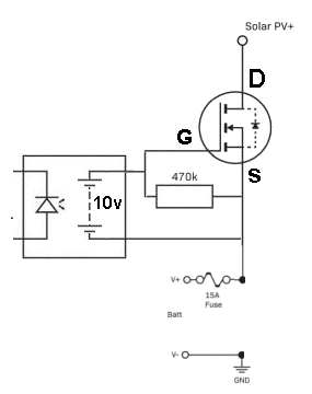
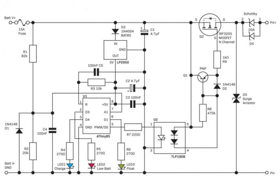
SOLAR CHARGER CONTROLLER
Here is a circuit from June 2021 of DIYODE Magazine.
When some LEDs receive very bright illumination they produce an output voltage
accompanied by a very small current.
In the following circuit, the OPTO-COUPLER has a bank of diodes on the output
that produces about 10v and a current of 10 microamps. This is not obvious
from the diagram and you have to reference the component date to see its
features. The top of the stack of diodes is positive but it not obvious that the
opto coupler is connected around the wrong way.
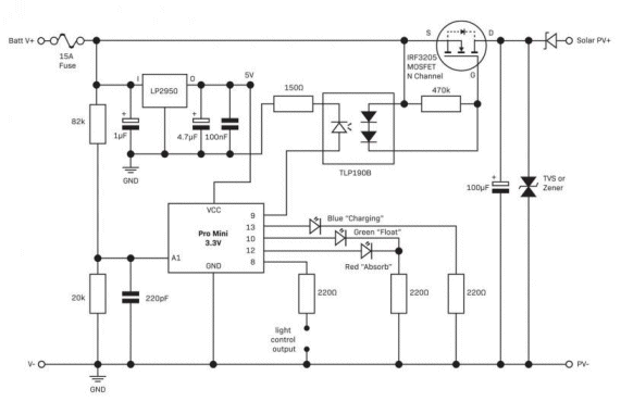
This is the part of the circuit we are discussing:
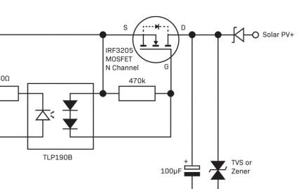
The circuit has been rearranged so you see the MOSFET with a
positive voltage on D
and a lower voltage on S. In addition you can see the
negative output of the opto-coupler is connected to G
and this will not turn on the MOSFET.

Here is the correct connection to the OPTO-COUPLER.
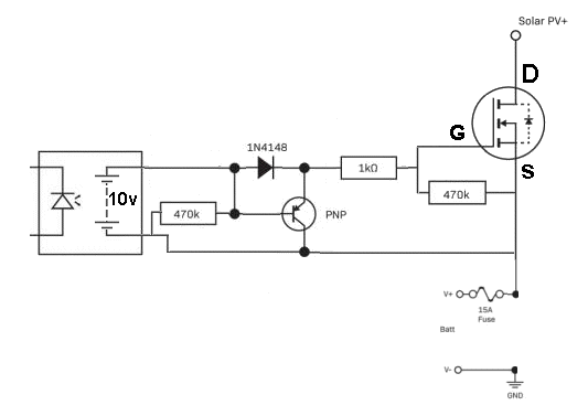
This modification is supposed to speed up the signal from the
opto-coupler.
I cannot see how it works, and I say it does not work, so I have sent the
request to Scott Williams, the technical editor of DIYODE for a clarification.
scott.williams@xentron
He has not replied to me.
Here is how the circuit works. Let us suppose the 10v from the opto-coupler
rises slowly as the circuit is supposed to turn on at some special point.
When the 10v is say 3v, the base will be 3v and the emitter will be 2.5v
For the transistor to turn ON, the emitter has to be higher than the base.
When the voltage rises to 10v, the base will be 10v and the emitter will be 9.5v
So the transistor NEVER TURNS ON.
However the 10v from the opto coupler goes through the diode and into the Gate
of the MOSFET and turns it ON.
The transistor does NOTHING.
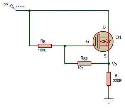
HIGH SIDE MOSFET
Here is a stupid circuit from EngineerGarage.com
They are trying the explain High-Side connection of MOSFETS. But if the 5v
supply is capable of delivering current to the load, what is the point of
including the MOSFET !!!!!
LED INVERTER
Here is a circuit with a number of problems. Apart from the fact
that is overly complex, the question is: why would you want to produce 330v DC
for a LED lamps when most lamps operate on 5v from a USB connection??
And 240v LED globes work on 240v AC !!
The other question is: why select an expensive transistor? The only two
sources on the web are $7.50 each or 10 for $30.00!!
The circuit is designed for 7watt output, so why use a transistor capable of
handling 5 amps?? But if you design the circuit to pass 5 amps, the
voltage across the transistor will be 1v and the losses will be 5 watts and yet
the transistor is the size of a BC547 and the data sheet says the transistor
will handle 1.5 watts. I would like to see a BC547 dissipating 1.5
watts !!! Maybe it will dissipate 300mW.
The whole idea of selecting a common transistor is to allow the hobbyist to
build the circuit from readily-available components.
The circuit is only suitable for 4v operation
To build this circuit you will need to know a lot about ferrite core
transformers. The primary winding is 16 turns for 4v. Making it 4
turns per volt, The secondary is 1360 turns, making the output 340v AC. I
don't know why you want 330v DC. What LED lamp operates on
330v DC????
The feedback winding Nf appears as an air core on the circuit, whereas it is
wound on top of the primary.
Removing the air gap is not a good idea. Without an air gap the
transformer can be saturated and the energising current will simply go into
heating the winding.
Where are you going to buy the wire with all the different diameters?
Finally the 10k pot is in a low-impedance part of the circuit and the value is
only suitable for a low power inverter. The value is too high for a
low-impedance section.
Here is a basic run-down on its performance.
The circuit takes 2 amps. The voltage across a transistor is 1v. This
gives the transformer 3v. The gain of the transistor is 100. The base
current will need to be 20mA. The output of the feedback winding will be 3v
minus the diode drops of 1v. You have 2v remaining. The pot resistance
plus the 68R must be 100 ohms. The pot must be 32 ohms !!! How
are you going to select 32 ohms from a 10k pot !!!! The whole
circuit is so impractical !!!
It can be simplified by cross-coupling the bases of the two transistors
to the primary winding and using base resistors.
The whole idea of putting a circuit on the web is to help hobbyists produce a
worthwhile project as cheaply as possible with readily-available components.
There are a lot of cheaper, simpler designs, that I would recommend.
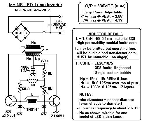
I can "see" how the whole circuit works and since there are no timing
capacitors, the frequency depends on how fast the magnetic flux increases to a
maximum in the core of the transformer.
The only component that cannot be "visualised" is the inductor between the bases
of the transistors. The note says it increases the frequency to 20kHz, but we
don't know the frequency before the inductor is fitted or the impact on the
efficiency. Normally one end of an inductor is fixed and the other end is raised
or lowered so that the inductor stores energy. In this case, one end can only be
raised 0.7v and the other end can be raised to the same value. You would need to
test the circuit with an Oscilloscope to see the result.
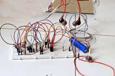
ELECTRONICS FOR YOU June 2023
We are constantly being bombarded to get projects done in India.
Here is a recent project from an Assistant Professor !!!! It is just
a piece of Junk !!! No-one can follow the circuit.
I have no idea what it does. And neither does anyone else.
For a few extra components you can achieve
constant volume as shown in the circuit below.
Here is his bio:
RAKESH JAIN received a Master�s degree in VLSI, B.E. in electronics and communication,
and DIPLOMA in electronics. He is currently working as an Assistant professor in
ECE department at Geetanjali Institute of technical studies, Udaipur. His
research area is SENSOR and Microcontrollers. He has 26 copyright and 3 Indian
patents. He has also been honored with Mewar Scientist Award2023.
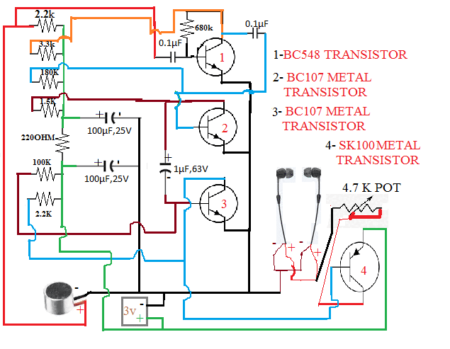
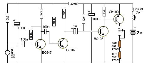
Here is the circuit, properly drawn, so you can see and understand how it works
and see the faults in the design.
The design of the circuit shows no understanding of electronics. It is not
sufficient to bundle a lot of components together, and if the circuit works,
publish it.
Someone, like me, who has had 50 years of designing circuits is going to see the
mistakes and problems and pull the circuit apart.
No thought has been put into the current taken by the circuit and this is one of
the most important factors in a good hearing aid design. Hearing aid
batteries are very expensive.
The 3rd and 4th transistors are directly coupled and 3rd transistor is going to
allow 3mA to flow through the emitter-base of the 4th transistor. A
current-limit resistor is needed to reduce the wasted current. The other stages
have high quiescent currents and the whole circuit should be redesigned. Stages
should be "self-biased" to get them into the centre of their operating range.
Not turned-on by any value base resistor you have in your "junk box."
Putting a 4k7 pot on the earpieces is going to reduce the output enormously.
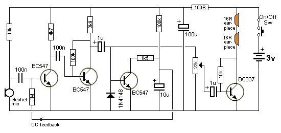
HEARING AID with CONSTANT VOLUME
PUSH PULL AMPLIFIER
Here's an amplifier with an unexpected feature. It is the connection of the
base resistor to Q2. Instead of it being connected to the positive rail,
it is connected to the speaker.
This produces a surprising effect.
We start with Q3 turned ON via Q1 and the speaker receives current as the 470u
electrolytic is charging. Eventually it will have a voltage almost equal to rail
voltage across it. During this time, Q2 will not be turned ON because the D1 is
keeping the base LOW.
Q1 starts to turn OFF and this puts less "pulling effect on the base of Q3 and
the transistor starts to turn off because basically the emitter lead will not
rise because the 470u is changed.
However the base of Q3 can rise and D1 allows the base of Q2 to rise via the
470R resistor. This turns ON Q2 and the emitter follows the base and pushes the
470u higher. This keeps occurring and the speaker "flips over" and now
the current flows in the other direction and this pushes the cone in the
opposite direction.
Normally, when the transistor modes to wards the supply rail, the voltage across
the base resistor reduces and the transistor has less effect. But by
connecting the resistor to the speaker, it still keeps the transistor turned on
until the electrolytic is discharged. This produces slightly better performance
than if the base resistor is connected to the supply rail.
The electrolytic can be thought-of as a battery to make the circuit easier to
understand.
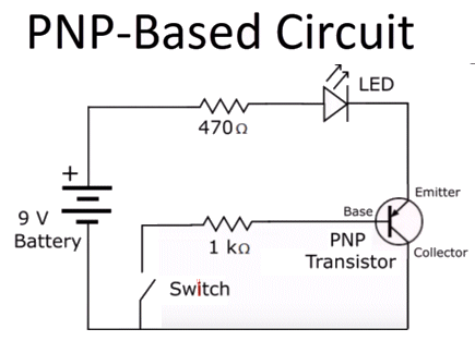
PNP CIRCUIT
Here is a PNP circuit from YouTube. The instructor said to replace an NPN
transistor with a PNP transistor.
But the circuit is wrong. It will work, but the transistor needs an emitter-base
voltage of .7v for the device to turn ON and this means the emitter-collector
voltage will a minimum of 0.7v. Normally the emitter-collector
voltage will be less than 0.2v and so the transistor will get hotter than normal
if the voltage rises to 0.7v or more. The base cannot be a 0v as this will not
allow any current to flow through the 1k resistor and turn the transistor ON. So
the emitter-collector voltage increases a small amount and now the 1k has a
small voltage across it and base current will flow. The emitter-base voltage was
measured as .697v and the base voltage .026v and the emitter-collector voltage =
0.723v
If you put a more powerful LED in the circuit and decrease the 470R to say 100R,
the emitter-collector current will increase and the transistor will demand more
base current. It does this by increasing the emitter-collector voltage to about
1.1v so that the emitter-base voltage of 0.7v leaves 0.4v for the voltage
across the 1k.
But now we have a voltage of 1.1v across the transistor and it gets very hot.
Here is the correct way to connect the PNP transistor:
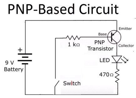
The emitter-collector voltage will close to 0.3v and the transistor is allowed
to operate correctly, over a wide range of current.
Here is a circuit from Ekeeda (an on-lime learning institute in India). They are describing,
discussing and explaining how it works. But it does not work.
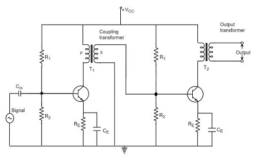
The output of the first inter-stage transformer will be only a few ohms and to
deliver enough current through the winding to turn on the second transistor will
require very low base-bias resistors. These will be so low that most of the
signal will be lost in them.
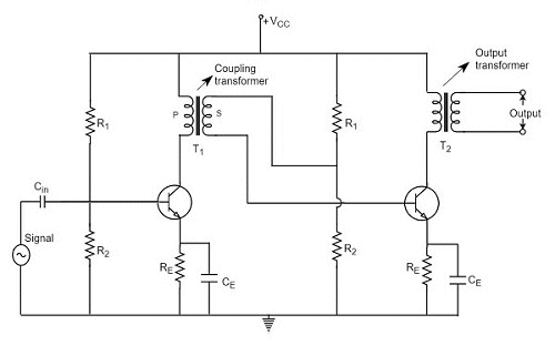
This is how the transformer should have been connected. No-one understood the
mistake and they all found the video very helpful. This is why no-one is being
taught electronics on YouTube. The instructors don't know and those
watching the videos are just being fooled with complexities or faulty circuits.
LATCH CIRCUIT
There is no fault with this circuit but the instructor said the circuit comes ON
with the LED illuminated and it would require another transistor to change this
state.
A low value electrolytic across the collector-emitter of the first transistor
would delay the turn-ON and create this condition and it is an exercise for you
to try different values and see if this will work.
ON-OFF
Here is an ON-OFF circuit from YouTube where the author has not
learned much
about electronics.
Firstly, I could not work out what the circuit does until I redrew it in the
conventional way.
You must draw a circuit so you can instantly see what each component is doing.
This requires the positive rail at the top so you can see the voltage-drop each
component.
The circuit must be at the beginning of an article as it lets you know what it
is doing and you can decide if the project is of interest to you.
CONTINUITY TESTER
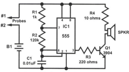
Here is a JUNK circuit from ETron Circuit Labs, who are trying to sell a
JUNK electronics course for $52.95 usd to unsuspecting hobbyists who do not know
what JUNK instructions looks like.
The Continuity Tester circuit above contains ALL the faults and mistakes that a
beginner could make.
For a start, the 555 does not work below 6v and the output is capable of
delivering 300mA so the transistor and components are not needed.
The website shows a 9v battery connected to the circuit. The circuit
symbol is not correct for 9v battery.
A small speaker (8 ohm) will overload the output and it must be connected via a
10u electrolytic to prevent excess current.
But the biggest mistake is the position of the probes. All the current of
the circuit will pass through the component you are testing and if the component
is delicate, it will be destroyed.
This circuit is an absolute disaster.
Triangular Output
Here is a circuit that only worked when you increase the resistance of one of the
resistors.
And the output is nothing like a triangular waveform.
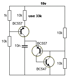
This is not how you design a reliable circuit. Circuits must be quite
independent of voltage, transistor type and resistor values. The more tolerant
it is, the more reliable the circuit will be.
The circuit did not work but by changing the 10k to 33k, a very unusual output
was obtained. There was no output point identified on the YouTube video but a
probe across the 10n and on the join of the two 10k resistors showed some
unusual results.
ORGAN
Here is another JUNK circuit from ETron
Circuit Labs.
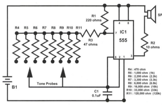
I am picking out these circuits because they want to charge $70.00 for a
JUNK basic Electronics course from people who don't have the slightest idea how
to design circuits. You can find all their circuit on the web and there
are hundreds of FREE electronics courses.
The main fault is the 10R in series with the speaker. The circuit is
powered from a 9v battery and if you use an alkaline battery, it will deliver
over 1 amp when heavily loaded.
The 8R and 10R will take over 500mA if the output of the 555 was able to supply
this current. But it can only supply 300mA and when you ask for a higher
current, the output transistor does not fully turn-on. This mean it has a
voltage across the output and 0v rail and when 300mA flows, the heat generated
in the output transistor is excessive and the whole IC will get quite hot.
It does not matter they used a cheap, junk, Indian battery that was old and
useless and their 555 did not get hot.
They present themselves as a teaching program and as such they should have an
understanding of circuit design. This, they have NOT.
TRIPLER
Here is a Tripler circuit from the web. You cannot trust the
web. The circuit does not work.
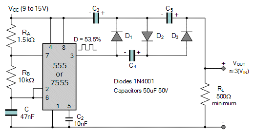
To understand how a capacitor gets charged, you have to look at the following
circuit:
The 22u on output pin 3 gets charged when the output is LOW via the top diode.
When pin 3 goes HIGH the top diode does not allow current to flow from the
capacitor to the power rail.
This means the only path is the lower diode.
However, the lower 22u is already charged to to nearly supply rail by the two
diodes, allowing current to flow to the electrolytic and charge it to nearly
supply voltage. This means it is already charged to 15v.
The fully-charged 22u on pin 3 gets "lifted up" by the action of pin 3 and the
left lead has say 15v on it and the capacitor has a charged voltage of 15v
between its two leads. This means the right-hand lead is nearly 30v above the 0v
rail and thus the second 22u gets charged from its present condition of 15v to a
final voltage of 30v.
For this action to occur, we need a capacitor that gets charged and then gets
"lifted" so that it can pass its energy into another capacitor. This
action is called a "CHARGE PUMP."
The diodes are called "gating diodes" as one diode allows the capacitor to
get charged and the other diode allows the charge to be passed to another
capacitor. Each is like a "one-way" gate.
You must have these 3 features to be present for the CHARGE PUMP to occur.
In the following circuit, diodes "a" and "b" and electrolytic "a" create a
Charge Pump to charge capacitor "b" to about 22v.
Capacitor "b" is called a STORAGE CAPACITOR. It is just like the 12v rail, but
it is 22v.
We now have the second Charge Pump section consisting of capacitor "c" and
diodes "c" and "d."
Capacitor "c" moves up and down by an amount of 15v via pin 3. When pin 3 is
LOW, it gets charged by capacitor "b" and then it is "lifted up" by an amount of
15v via pin 3 and this extra voltage is passed to capacitor "d" to create a
final voltage of about 31v.
This voltage is not produced after one cycle or even 2 cycles. It takes many
cycles. This is because capacitor "c" takes energy from capacitor "b" and it
takes many cycles for the capacitors to gradually charge. That's why the Charge
Pump circuit takes a few seconds to deliver the 31v.
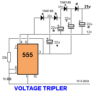
Now you know how the Charge Pump circuit works, you can see the first Tripler
circuit only doubles the voltage.
The first stage consist of capacitor C3, C4 and diodes D1, D2.
C3 is charged via diode D1 and when pin 3 is low, C4 is charged via D2 from C3.
But C3 is never charged to more than 15v and the first Charge-Pump stage does
not see voltage doubling. The second section creates voltage doubling and that
is all you get on the output.
C LASS-A
AMPLIFIER with transformer
This is another mistake from a discussion on YouTube.
The instructor said the polarity of the voltage on the primary winding of the
transformer reverses during the second part of the cycle and he says the voltage
on the collector will rise above 12v.
This is not true.
I know this is very complex to understand and that's s why so many mistakes are
made.
When the transistor turns ON, the current through the primary winding produces
flux in the core of the transformer and the top lead will be 12v and the lower
lead will be about 4v.
This is the incorrect way to describe the circuit:
When the transistor turns OFF, it effectively disappears from the circuit and
the flux in the core collapses and produces a voltage on the primary winding
that is OPPOSITE to the original voltage. This voltage can be 10 times higher
and even 100 times higher.
This action is due to the natural and fast collapsing of the magnetic flux
(field) and we call this effect FLYBACK.
During this time the voltage on the secondary will firstly be in one direction
and during the second half of the cycle it will appear in reverse at a much
higher value.
BUT this is not the case in the circuit.
The circuit is not a FLYBACK arrangement.
It is an audio amplifier and the transistor does NOT turn OFF or
disappear.
It is always connected and it always controls the increasing and decreasing
current through the primary winding.
This action is completely different to FLYBACK.
When the transistor is turning ON, the flux in the core increases and produces a
voltage in the secondary winding with the output voltage as a positive on the
top wire.
When the transistor turns OFF, the flux is reducing and produces a negative
voltage on the top wire of the output.
In other words, the output sees a reversal of voltage during this complete cycle
(the secondary voltage) and it is not very high - or may not be very high
- as it determined by the turns ratio of the number of turns on the primary and
the number of turns on the secondary.
So, the secondary voltage may reverse but the primary voltage simply decreases
and increases.
That's the amazing part, you can get a reversal of secondary voltage via two
different ways and that's why so many people get confused.

Page 1
Page 2
Page 3
Page 4
Page 5
Page 6
Page 7
Page 8
Page 9
Page 10
Page 11
Page 12
Page 13
Page 14
Page 15
Page 16
Page 17
Page 18
Page 19
Page 20
Page 21
Page 22
Page 23
Page 24
Page 25
Page 26
Page 27
Page 28
Page 29
Page 30
Page 31
Page 32 |