|
Wireless Doorbell |
An educational
project using a $10.00 doorbell
No kits are available for this project
9-9-2006
13-1-2019 - 5k6 added to circuit
You cannot beat the Chinese.
The project described in this article is a ready-made item from a $2.00
shop! And it is made in China!
It is a wireless doorbell with a cost of about $10.00.
It is so cheap, you could not build it from components for $10.00!
So, we have to change our attitude to building projects and use items such as
this to learn how things work and modify them to suit our own
requirements.
This doorbell uses quality components. It's not rubbish. The circuit is
quite unbelievable. You can not obtain some of the components individually and
the effectiveness is magic. We have so much to learn!
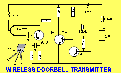
Here is the corrected circuit:
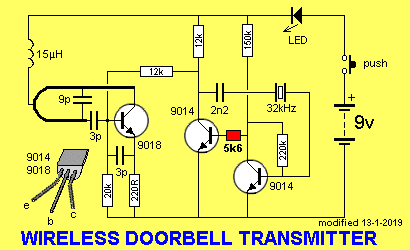
5k6 needed to allow the voltage on the second transistor to rise above
0.65v
| Transistor Type: | Collector current: | Max frequency |
| 8050 NPN | 1.5A | 100MHz |
| 8550 PNP | 1.5A | 200MHz |
| 9014 NPN | 150mA | 150MHz |
| 9018 NPN | 50mA | 700MHz |
The first thing you will notice is the clever
circuitry. Some of the design goes against everything we have learnt in
electronics.
That's why we have to study other people's designs and realise "the more
you know, the more you realise you don't know."
The oscillator circuit is very interesting, but first we will look at
the RF oscillator.
The doorbell operates on the 303MHz band and the 30 metre range (100ft)
is obtained without the use of an antenna! The circuit is actually
radiating from the printed track of the tank circuit. The Tank Circuit
is a single-turn coil and a
small capacitor (5p & 4p in parallel).
In this project we show how to add a small antenna to the circuit
to get double the range - plus two other improvements to increase the
range.
Some of the improvements will load the circuit and alter the
frequency at which it operates. Others can be done without any effect on
the circuit.
Fortunately, the transmitting stage is what we call "tight" and is not
affected by surrounding "stray capacitance."
Normally, this stray capacitance is a persons hand or body, touching or
coming near the transmitting (output) stage and altering the frequency.
The circuit has been kept near the power rails by the use of a choke in
the positive rail. The positive rail is then reflected to the negative
rail via the battery.
This feature helps us when we want to add an antenna.
A 7cm length of tinned copper wire is connected to the collector of the
transistor and bent around the board so that everything can be put back
into the case.
When the project was tested inside the authors house, the range was
increased to double.
When the transmitter was taken outside, the range was over 60 metres
(200ft) and the full range could not be tested as the sound from the
doorbell was too faint to be heard!
We can learn so much from a product that is already on the market.
Firstly, you know it works, it is reliable and you know what can be
built for $10.00.
Secondly, you know what type of components can be purchased cheaply and what
to expect from them.
In this case the transmitting transistor has the highest gain - so they
have taken a special effort to get a good quality transistor.
Now, let's look at the transmitter circuit:
The transmitter circuit is made up of two building blocks - the 303MHz RF oscillator and the 32kHz crystal controlled oscillator.
The 303MHz oscillator consists of a self-oscillating circuit made up of the coil on the PC board and a 9p (9 puff) capacitor (actually 4p and 5p in parallel).
The circuit starts-up by the transistor producing noise. This rising-and-falling signal on the collector is passed to the parallel tuned circuit (the tank circuit) and the base sees a very smooth sinewave at a frequency of 303MHz.
This sinewave is then amplified by the transistor and this is how the 303MHz frequency is generated.
Now we come to the purpose of the 15microhenry choke on the tank circuit.
When the circuit oscillates, it takes a larger and small amount of current.
This current passes through the choke and the turns produce a back-emf or back voltage that fights against the flow (change) in current. The end effect is a voltage created at the point where the choke is connected to the track-work on the board. This effectively allows the track work to produce a waveform and since the frequency of this wave is very high, a percentage of the energy is radiated into the air as electromagnetic energy.
The choke allows the track-work to effectively rise and fall while providing a very low resistance path for the flow of current during certain parts of the cycle.
The second building block is the crystal oscillator.
This is made up of a two-stage DC coupled amplifier with feedback via the 2n2 and crystal.
If the crystal is removed, the oscillator is seen as producing very narrow spikes with a frequency determined by the 2n2, as shown in the diagram below:

When the crystal is added, the frequency increases (because the effect
of the 2n2 and crystal in series creates a lower capacitance than 2n2) and as it rises, the
amplitude of the feedback signal increases until it reaches a maximum at the resonant
frequency of the crystal. The crystal exhibits the lowest impedance (the
highest capacitance) at the resonant frequency. This is how the circuit stabilizes at the
frequency of the crystal.
When the device is turned on, the 150k on the base of the second
transistor turns the transistor on.
The third transistor has 0.65v on the collector and the base also
receives very close to 0.65v, via the 220k resistor.
The third transistor is not fully turned on and it produces a small
amount of noise. This noise is passed to the second transistor and
appears on the collector. The collector passes this noise to the base of
the third transistor and the noise very rapidly increases to a maximum.
It comes to a point where the waveform above is generated and the reason
why the spikes are so narrow is easy to explain.
When the middle transistor changes from an OFF state to an ON state, the
capacitor will be partially charged and the voltage on the end connected
to the base of the third transistor will drop about 6v and put a
negative voltage on the base of the third transistor. This will keep it
off and the middle transistor will be kept ON via the 150k
base-resistor.
The capacitor will gradually charge in the opposite direction via the
220k and 150k and when the base of the third transistor sees about 0.6v,
it begins to turn ON.
This causes the middle transistor to turn OFF and the collector voltage
rises. This causes the capacitor to charge and create a current-flow in
the base of the third transistor. Both transistors are now turned ON and
the capacitor charges very quickly via the 12k and base-emitter junction
of the third transistor. This creates the very narrow high-period in the
waveform.
When the push button is pressed, the circuit produces a 303MHz carrier
with a 32kHz tone.
The receiver detects the 32kHz and turns on a SOUND chip.
THE RECEIVER CIRCUIT
The receiver circuit consists of a number of stages and we will go
through each one separately.
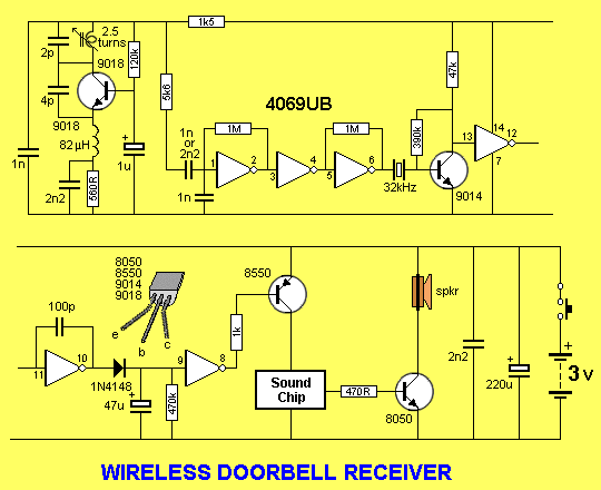
The first stage is actually a 303MHz oscillator that is operating all
the time.
It produces a clean 303MHz signal and this frequency is too high to be
detected or processed by the 4069 chip, as the chip will only operate to
about 1MHz.
The theory behind using this type of stage is quite simple.
It is easier to "upset" or modify a stage that is already oscillating,
rather than get a non-oscillating stage to begin oscillating.
There are all sorts of electromagnetic radiation at 300MHz and the 2-turn
coil picks up all this noise.
The 303MHz oscillator is firstly set into operation by the noise
produced by the transistor and this is passed to the tank circuit made
up of the 2-turn coil and 2p capacitor as a parallel tuned circuit. The
transistor keeps amplifying this until it gets to a stabilized point
where the collector is producing "hash" (junk) of about 300mV.
When the transmitter is activated, the receiver circuit will detect a signal as small as
a few micro-volts and the 32kHz signal will be included with all the
other noise.
There is a little bit more behind this receiving stage, than first meets
the eye.
The stage is actually a transmitter, but we will still call it the
receiver circuit. Yes, it is a very weak transmitter
and it fills the surrounding with a clean 303MHz signal. When the 303MHz
signal from the transmitter enters this space, the signals interfere
with one another and the receiver takes more and less current as
it tries to maintain the signal strength. When the 32kHz
signal is present, the receiver takes a varying current that corresponds
to the 32kHz signal and this is how the receiver circuit produces the
waveform to correspond to the 32KHz.
A low-impedance path to the 0v rail is provided for the emitter by using
a 82uH choke and a 2n2 capacitor across a 560R resistor.
This low impedance path is needed so that the transistor has a high
gain.
The circuit is put into very delicate oscillation by using a 1k5 from
the positive rail.
It operates from 3v and the current taken by this stage is less
than 1mA.
THE BRASS TUNING-SLUG
The coil in the tank circuit is tuned via a brass screw (or slug or
core).
This is alters the frequency at which the circuit operates, when it is
turned via a small screwdriver.
At 303MHz, you cannot use a ferrite core as it will completely absorb
the magnetic radiation produced by the coil and prevent the circuit
operating.
Another choice is air. If you use an air cored coil, you can use a
trimmer capacitor to adjust the frequency. A cheaper approach is to use
a brass core. Brass has a permeability very close to air (�0
is the permeability of free space) and it has very little effect on
concentrating the magnetic lines of flux or moving them apart.
Materials that cause the lines of flux to move farther apart,
resulting in a decrease in magnetic flux density compared with a vacuum,
are called diamagnetic. Materials that concentrate magnetic flux by a
factor of more than one but less than or equal to ten are called
paramagnetic; materials that concentrate the flux by a factor of more
than ten are called ferromagnetic.
However, at very high frequencies, such as 303MHz, the magnetic flux
causes eddy currents to flow in the brass and this decreases the
available flux so that inserting a brass core causes the frequency to
drop.
This is how the receiver is tuned to exactly the same frequency as the
transmitter.
The most critical capacitor in the receiver is the 2p. This sets the
frequency. The 4p is merely a feedback capacitor.
The 2n2 and 1n are
called "pass" capacitors and allow high frequency signals to pass
through them. The 1n actually keeps the positive and
negative rails rigid while the 2n2 prevents the emitter moving up and
down when amplifying the 303MHz signal.
The signal on the collector passes to the first input of the chip via a 5k6 resistor and
1n (pass capacitor).
A lot of the high frequency component is removed with the 1n capacitor
connected to the 0v rail.
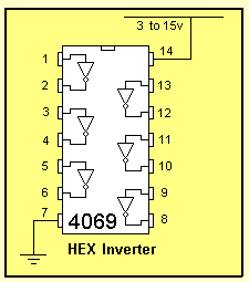
The first inverter has a 1M connected between the output and input to
set it to mid rail so it becomes a high-gain amplifier.
The second and third inverters also amplify the signal and on pin 6 we
have a signal greater than 0.6v containing a lot of noise and an
identifiable 32kHz waveform.
The 32kHz crystal only allows the 32kHz signal to pass and the base of
the transistor sees a very clean signal. Any other frequencies will not
appear on the base of the transistor. The 32kHz is further amplified with two more stages and appears at pin 10 of
the chip.
It is then passed to a diode pump that charges a 47u electrolytic.
Normally, this electrolytic is uncharged and pin 8 is HIGH. The PNP
transistor is not turned on and the sound chip is silent.
But when the electrolytic charges, the transistor turns
on and the sound chip operates.
GOING FURTHER
One of the main reasons for presenting this project is to show how to
get the best range from a transmitter.
Normally you need very expensive equipment to help you, but
a very clever alternative is to use our method.
All you have to do is place the receiver about 15 metres from the
transmitter and in a very poor reception area.
The aim is to get the receiver to be at the extreme end of the range so
that if you move the transmitter away by as little as a metre, the
receiver will not detect the signal.
Now the receiver is a very sensitive RF indicator. By moving the
transmitter to different places, the receiver should
not detect the signal.
You are now ready to add an antenna to the transmitter and determine its
effectiveness.
We have already mentioned the transmitter circuit is classified as
"tight" and adding an antenna should not shift the frequency.
ADDING AN ANTENNA
The 7cm antenna is added to the point where the choke touches the PC
coil on the board.

Adding the 7cm antenna
This point is highly active but it does not interfere with the
operation of the circuit, when the antenna is connected.
The circuit turns ON via the 22k resistor and this is
because it puts a voltage on the base that is 0.7v higher than the
emitter. The current delivered by the 22k can now turn the transistor
ON a certain amount - BUT it is not allowed to turn the transistor ON
fully. If it did, the other components in the circuit (that turn the
transistor ON - by an increased amount) would not be needed and there
would be no components in the circuit to turn it OFF.
The circuit above is called an LC HIGH PASS FILTER.
Bend the wire around the edge of the board and about 0.5cm above it and test the transmitter. You
should get an increase in the range, up to double.
If the range does not increase appreciably, the receiver may not be tuned
exactly to the transmitter. To do this, adjust the brass screw in the
tank circuit of the receiver.
Before making any adjustment, make sure you know the original position
by noting the alignment of the slot.
Only turn the screw about 15� in
either direction and take a "field test." If the range reduces, you
know the screw has been turned in the wrong direction.
INCREASING THE OUTPUT
Another thing that will increase the output of the transmitter involves
rewiring the LED.
At the moment the LED is in series with the positive rail of the
transmitter.
This effectively drops about 1.7v and the circuit only gets 7.3v from a
fresh battery.
By connecting the LED between the positive and 0v rail, with a 470R load
resistor, the transmitting section will see 9v and this will increase
the range.
One more thing that will increase the output is to add a 220R across the
220R emitter resistor of the transmitter transistor.
This increased the range in our prototype, but the frequency-adjusting screw on the
receiver had to be turned about 15�
clockwise to compensate for the slight change in frequency.
THE 82uH INDUCTOR IN THE RECEIVER
I covered the amazing improvement of
adding an
inductor in the emitter circuit of a transistor in Spy Circuit Page 1.
I am not going to re-write the discussion but merely copy it onto this
project and you can work out the relevance.
It's the inductor in the emitter. This can be in a transmitting
circuit or receiving circuit.
Let's look at what is does and how it works.
The following circuit is a common-base COLPITTS circuit and oscillates
at 303MHz.
The components that set this frequency are: the length of the track on
the PC board (shown in thick black) and the value of the capacitor
across this track.
The component that makes this a "common-base" circuit is the capacitor
on the base.
The 1n has a capacitive reactance of less than ONE OHM at 303MHz!
This means the base will not move up and down during the time when the
stage is oscillating.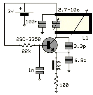
So, we have the first part of the cycle where the 22k starts to turn the
transistor ON.
Before we go any further, we have to mention the second way a transistor
can be turned ON.
If we hold the base of a transistor rigid and "pull" the emitter lead
towards the 0v rail, the "gap" between the base and emitter will
increase and although this increase may be only a few millivolts, it
will cause the transistor to turn on MORE.
Now, there is one more thing we have to cover.
When the voltage on the collector falls, due to the transistor turning
ON, the energy in the 3p3 will be passed to the emitter to reduce the
voltage on this lead.
But there is more to this. When the transistor turns ON, the relatively
high voltage across the 3p3 will be converted to a much lower voltage to
push the emitter lead a few millivolts lower but the current it will
deliver will be considerable.
The emitter lead is considered to be a very low impedance lead and it
requires a considerable current to move it lower.
Let me explain the capacitor phenomenon again:
You already know about this phenomenon, but have forgotten.
If you take a large electrolytic and charge it on a 12v battery with a
resistor in series, the capacitor will take a long time to charge and
the current-flow will be quite small.
Now take the electrolytic and short the 2 leads on the shaft of a
screwdriver. You will see a bright flash and the screwdriver will be
"burnt."
That's because the electrolytic is capable of receiving a low current
over a long period of time and releasing a high current for a short
period of time.
The 3p3 is doing the same thing.
The low impedance of the "emitter circuit" is due to two things. It is
due to the junction inside the transistor and the 100 ohm resistor.
If we were able to remove the 100 ohm resistor, the impedance of the
"emitter circuit" would increase - but obviously the circuit would not
work.
If the impedance of this part of the circuit is increased, the 3p3 will
be able to turn the transistor ON more and thus the overall amplitude of
the circuit will increase.
That's exactly what the inductor does. It effectively moves the 100 ohm
resistor away from the emitter lead so the 3p3 sees the "emitter
circuit" as a higher impedance.
How does it do this?
Firstly you have to understand how an inductor works when placed in this
type of circuit. 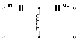
It only allows high frequency signals to pass through the filter.
The signal enters from the left and the left lead of the first capacitor
rises and falls and passes this action to the right plate.
The incoming signal is not reduced by the capacitor if the signal has a
high frequency.
This means the incoming signal appears on the top of the inductor with
very little attenuation.
When the signal rises, a small amount of current enters the inductor and
produces magnetic flux. This flux is called EXPANDING FLUX and it cuts
all the other turns of the "coil" and produces a voltage in these turns
that is of opposite polarity to the incoming voltage. Say the incoming
voltage is 10v. The inductor will produce a voltage of 9.999v and this
means only 1 millivolt is available to deliver a current into the
inductor.
The end result is this: only a very small current will flow into the
inductor.
Exactly the same thing will happen when the voltage is falling.
The inductor will have very little "grip" on the voltage and it will
allow the voltage to "pass over" the inductor without reducing its
amplitude.
The "out" capacitor will pass the amplitude without reducing it and so
the incoming waveform will pass though this circuit without being
effected.
If the waveform has a low frequency, the first capacitor will attenuate
it and the inductor will reduce it and the "out capacitor" will reduce
it. The output will be almost zero.
Now, how does the inductor in the 303MHz circuit work?
It allows the signal from 3p3 to enter the emitter lead and have very
effect on attenuating the amplitude.
If the inductor were just a short length of wire, it would not have the
same effect and a lot of energy from the 3p3 would be passed to the 100
ohm resistor.
I know the two circuits are not identical, but the basics are still the
same.
The addition of an inductor DOUBLED the range of another transmitter
circuit we were testing in the laboratory and when you realise the extra
power needed to do this (about 8 times), its effectiveness is very
impressive.
22-10-2014
13-1-2019