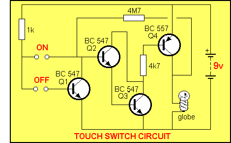
THE DARLINGTON TRANSISTOR Mouse-
The TOUCH-PADS deliver current from the power rail to the
input of the circuit, via a moist finger. The finger acts as a very high
resistance but it will allow enough current to flow to turn the circuit
ON. THE
SUPER-ALPHA PAIR
The diagrams above show two transistors connected
as a SUPER ALPHA PAIR. The first diagram is taken directly from the TOUCH
SWITCH circuit and the second is re-arranged slightly to show the standard
SUPER ALPHA layout.
The circuit turns ON
a lamp (or other device) when a very small current is delivered to
the input. In this case the current is provided by a finger,
touching two TOUCH-PADS. The circuit also has another feature. It
will "latch-on" and the globe will remain illuminated. A
second touch pad is provided to turn the circuit off.
over:
![]()
![]()
to see
circuit
work
As the circuit turns ON, voltage is developed across the globe and this
is passed to the "front-end" via a 4M7 FEEDBACK resistor. This
resistor effectively takes the place of your finger so that when the
finger is removed, the circuit will stay active.
To turn the circuit OFF, Q1 is made active by the OFF touch-pad and this
transistor removes the "turn-on" voltage to transistors Q2 and
Q3. This turns off the output transistor Q4 and the voltage across the
globe reduces. When the finger is removed from the OFF pads, the circuit
has completely turned off and absolutely no current will be drawn.
The only current taken when the circuit is off is called LEAKAGE CURRENT
and this will be LESS than 1uA and will flow through the junctions of the
BC 557 when the transistor is OFF.
This circuit is a vast improvement over the previous design and it can be used
for all types of applications where an electronic "latch" is required.
Transistors Q2 and Q3 are connected together in a
very special way. They form a single transistor with a very high gain and very
high input impedance.
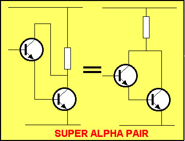
You can think of the two transistors as a single transistor. They behave
exactly like a single transistor except the only
difference is the turn-on voltage. It must be 0.6v + 0.6v = 1.2v as the two
base-emitter junctions are "on top of each other."
The other important feature of this arrangement is the high input
impedance.
Normally, the input impedance of a common-emitter transistor is about 2k to 5k.
When two transistors are connected in a super-alpha arrangement, the input
impedance is 200k to 500k.
What does this mean?
The best way to describe this feature is via a TIME DELAY. When a capacitor is charging,
current (energy) is being fed to it via a resistor. If we place a monitoring
device across the capacitor, some of the energy from the resistor will flow
into the monitoring device and the capacitor will not charge at the same rate
(It will take longer to charge).
If we need to monitor the voltage across the capacitor (to detect when it
reaches a certain value - to end a time-delay, for example) we need to place a
very light load across the capacitor.
The super-alpha arrangement is ideal for this. It imposes a very light lad on
the time-delay circuit. (You will need to place a resistor between the
time-delay circuit and the super-alpha transistor so that the capacitor will
charge above 1.2v (the base-emitter junction voltage of the super-alpha
transistor).
The high input impedance of the super-alpha transistor is needed so that the
circuit will detect a finger across two touch plates.
A finger pressing on two plates presents a resistance to the circuit and will
allow current to flow. Depending on the moisture content and pressure
applied, the resistance can be as low as 30k or as high as 1M. To get reliable
operation, the circuit must be able to detect a high resistance and thus a
very high gain stage is required.
Transistors Q2 and Q3 form a single stage with a gain of at least 100 x 100 =
10,000 and thus an input current of as little as 1uA (1 micro-amp) will allow
a current as high as 10mA to flow in the collector-emitter circuit.
The animation below shows exactly how the super-alpha arrangement works. As
soon as the voltage on the base rises above 1.2v, the "top"
transistor will allow current to flow into the base. The transistor is a
CURRENT AMPLIFIER and it allows about 100 times this current to flow in its
collector-emitter circuit.
At the beginning of the cycle, the lower transistor "sees" the upper
transistor as a very high resistance and it is not turned on.
When the "upper" transistor is turned on, the lower transistor sees
it as a low value resistor (a resistance of about 30k to 100k) and it is
turned ON.
The circuit sees the lower transistor as a very low resistance (about 1k) and
if the supply voltage is 9v, the current flow through the collector-emitter
circuit would be 9mA. But a 4k7 resistor has been included in this circuit to
limit the current less than 2mA.
This current is sufficient to drive the
output transistor into full saturation to turn ON the lamp.