|
THE |
|
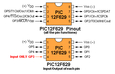
The microcontroller we will be using for the projects in this series is the
PIC12F629.
There are a lot of features in this 8-pin micro but we will keep things
simple by just using the pins for input and output.
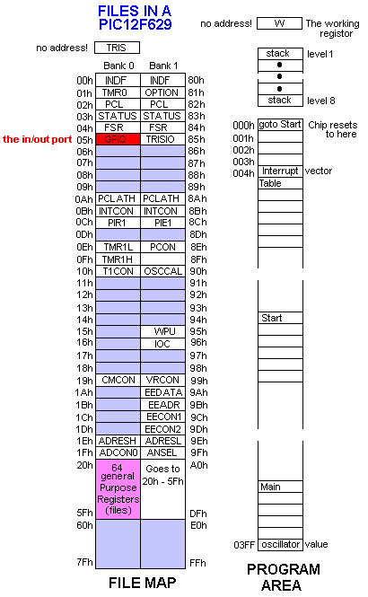
Here is a list of the files in the chip and the 1024 locations for your program:
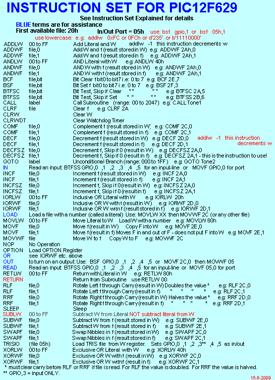
A microcontroller needs a file to carry data from one file to another. It's a bit like a "bus-boy" or "house-boy" that does all the carrying etc in a hotel. The was originally called the accumulator in early microcontrollers. It is now called the working register and given the letter "w." At the beginning of a program you need to create a number and load it into a file. You cannot load it directly into a file. It has to loaded into w then transferred from w to the file. The value (the number) is called a LITERAL "l" and put it into the WORKING REGISTER (called w), then moved to one of the registers. . . These registers are also called FILES. The two instructions are: movlw 7 - this instruction creates the value seven. It is: move the value seven to "w" movwf 20h - this instruction puts seven into file 20h. "w" is the working register (file) These Files or Registers are also called GPR's (General Purpose Registers) and once they contain a value, they can be incremented via a single instruction (incf) where "f" is the file number or decremented (decf 20h) or the contents moved left (rlf 20h) to halve or right (rrf 20h) to double the value of the file or a number of things. The input/output port (file 05) is just like one of these files (registers) but it is connected to 6 pins on the chip so that any value in this file will appear on 5 of the pins (pin 4 is an input-only pin). Before loading the input/output port, you must tell the micro to configure the port as an output by loading a value into the TRISIO register (85h) with a "0" for each pin that you want to be an output. You can simply load it with "00" and all 5 pins will be output or selectively load some of the pins: (1111 1011) and only GPIO2 will be an output. You can individually set (make = "1") any bit in any file (register) or clear (make = "0"). You can change all the bits to their opposite value by using the instruction, eg: comf 20h (complement f ) this will change: 1111 0000 to 0000 1111 or 1010 10101 to 01010 0101 When the input/output port is configured with one or more bits as "1" (for INPUT), the voltage on the corresponding pin can be read by your program, just like any of the other registers. You can pass the whole register to "w" or look at the individual pin and see if it is HIGH or LOW. This is called BIT TESTING (btfss 04,2) For example, you can test bit 2 (pin 5) to see if it is SET and if it is SET, the micro will jump over the next instruction and execute the following instruction. The full explanation of btfss 04,2 is: bit test 2 (test bit "x" in: 0000 0x00) of file 4 (the input/output port) and skip (jump over the next instruction) if is it SET (1). To test the bit to determine if it is CLEAR: btfsc 04,2 The CALL Instruction The CALL instruction for a PIC12F629 accesses ALL MEMORY. The STACK The PIC12F629 has an 8-CALL stack. (8-level stack). The In/Out Port The IN/OUT port on a PIC12F629 is file 05h. This port corresponds to pins 7, 6, 5, 4, 3, and 2 for GP0, GP1, GP2, GP3 GP4 and GP5. Remember: GPIO,3 (GP3) (pin 4) is an INPUT-ONLY pin. When writing a program, use GPIO,0 GPIO,1 GPIO,2 GPIO,3 GPIO,4 GPIO,5 in your program and the compiler will do the rest. (GPIO = General Purpose Input/Output). For instance, If you want to SET (make HIGH) pin 7, you must do two things: 1. Make sure GPIO,0 is an OUTPUT bit by making the corresponding bit in the TRISIO register "0." This is done via the following instructions: Remember: "0" = output, "1" = input bsf status, rp0 ;bank 1 movlw b'xxxxxxx0' ;(x= don't care = does not matter) movwf TRISIO ;the lowest bit will be an OUTPUT bcf status, rp0 ;bank 0 Make the lowest bit of the output port = 1 (HIGH). This is done via the following instruction: bsf GPIO,0 Do not set more than one bit at a time in the GPIO (in/out) port. In other words, do not create two instructions such as: bsf GPIO,0 bsf GPIO,2 If you need to clear or set two or more output lines, perform the operation via a single instruction, thus: movlw b'xxxxx1x1' movwf GPIO You need to know the state of all the outputs and include this in the value you are going to load into GPIO via movlw b'xxxxxxxx' etc. As can be seen from the above, the six lower bits of file 05 are connected to 6 pins of the chip to connect the microprocessor to the outside world. This file is like all the other files (from 20h to 5F - 64 files) as it can be operated-upon (incremented, decremented, shifted left or right, plus the other operations). The only difference is the contents of file 05 can be exported to the outside world and the outside world can influence the file. When any of the bits of file 05 are configured as "out," the value of the bit will make the corresponding pin of the chip either HIGH or LOW. When it is "set" (=1), the pin will be HIGH. When it is "clear" (=0), the pin will be LOW. READING AN INPUT LINE When any of the bits of file 05 are configured as "input," (this is done via the TRISIO instruction) the HIGH or LOW on the pin of the chip (this HIGH or LOW will be created by something in the outside world making the line HIGH or LOW) will be read by the micro as a HIGH or LOW, (when the file is read via an instruction such as btfss GPIO,1 or btfsc GPIO,1 - bit test1 in file 05h, skip if set or bit test1 file 05h, skip if clear). This "reading process" can also be done when the contents of file 05 (GPIO) is moved to W. The instruction to do this is movf 05h,0 This instruction tells the micro to move the in/out port to the working register. The working register is called "W" and has the destination "0" - a file has the destination "1." (or you can use ,w for the working register and ,f for a file. The assembler accepts either terminology). The contents can also be shifted, incremented - plus other instructions. Here are some instructions to read the input bit: In most cases, the first bit (or line or pin) to use in a program is pin 4 as this line is INPUT ONLY. It corresponds to GPIO,3. Using the instructions from above, we have GPIO,3 as an INPUT and all other lines are OUTPUT. We are looking for a HIGH on the input line. To read the bit, use the following instructions: btfsc GPIO,3 ;This will test the input bit and if it is LOW, the micro goes to movlw xx GOTO PhaseA ;This instruction takes the micro to a new sub-routine movlw xx If you don't know the state of some of the bits (or don't want to alter them - by mistake), you can use the XOR instruction. Here is what NOT to do: For example, to turn ON bits 0, 1 and 2, the instructions can be: bsf GPIO,0 b'00000001' bsf GPIO,1 b'00000010' bsf GPIO,2 b'00000100' This will result in only the third instruction being carried out. We mentioned above, not to use multiple bit-setting as it will fail to work. The answer is to use the XOR instruction Combine the 3 instructions to get: b'00000111' movlw 07h xorwf GPIO Only the three lowest outputs will go HIGH. To turn OFF the three lowest outputs, repeat the same instructions: movlw 07h xorwf GPIO Only the three lowest outputs will go LOW. Actually, the bits will TOGGLE. The in/out port (file 05h for PIC12F629) is shown in RED in the file map above. It is called GPIO: Voltage on an Input line Most input lines are classified as TTL and the voltage must be above 2v (for 5v rail) for the chip to detect a HIGH. GP2 is Schmitt Trigger input as it is TMR0 clock input. This line requires 2.5v to detect a HIGH and 1.75v to detect a LOW. TTL inputs have a small gap between HIGH and LOW and to make sure the input line detects correctly. There is a range of voltage between HIGH and LOW and LOW and HIGH so a definite HIGH or LOW can be determined. Reading the Input Port To read the individual pins of the input port of a PIC12F629, use one of the following instructions. (GPIO,3 (GP3) (pin 4) is an INPUT-ONLY pin and this pin is the first to use. If the input pin is normally low and goes HIGH when a signal is sent to the micro, use one of the following: btfsc 05h,0 (This the same as: btfsc GPIO,0) btfsc 05h,1 btfsc 05h,2 btfsc 05h,3 - this is pin 4 - GPIO,3 - use first in your program btfsc 05h,4 btfsc 05h,5 The next instruction will be: goto task1 - input has been detected It may be difficult to read the same input bit further down a program. This is solved by setting and clearing the bit, thus: bsf status, rp0 ;Bank 1 bcf TRISIO,0 nop bsf TRISIO,0 bcf status, rp0 ;bank 0 The General Purpose Files - called GPR's (General Purpose Registers) The General Purpose Files are the files you use in your program for sub-routines such as delays, comparison, incrementing, decrementing, etc. A program can start by loading a value into GPIO and outputting it to the outside world (such as a LED). A value (called a literal) is loaded into a file (a General Purpose File) and decremented until it is zero. This allows the LED to be viewed. The instruction set for the PIC12F629:
WRITING A PROGRAM movlw 10h or movlw 0x10 the next instruction will send the micro to the table: call table The micro will go to the table and add the value you have written (10h or 0x10) into w to the program counter. The instruction to do this will be the first instruction at the table:
addwf pcl,f ;02h,f add W to program
counter.
The Program Counter is file 02 (see
The next part of this discussion is:
The Experimenter PC Board.
ooo00000ooooo
27-5-2013 |