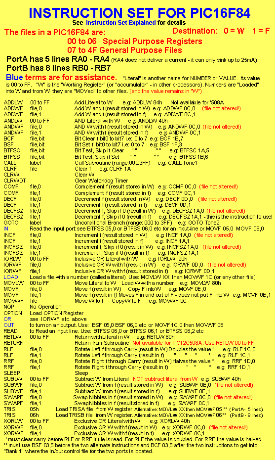
PIC16F84
Instruction-Set
| ADDITIONAL
INSTRUCTIONS ADDWF PCL,1 ADDWF 02,1 Alter the program counter to create a jump CLRF INDF,1 CLRF 00,1 Clear INDIRECT file INCF FSR,1 INCF 04,1 Increment the File Select Register INTCON address is either 0Bh or 8Bh - it is mapped at both locations. BCF INTCON,RBIF Clear RB<7:4> Port-change Interrupt flag BSF INTCON,RBIF Set RB<7:4> Port-change Interrupt flag BCF INTCON,RBIE Disables the Port-change Interrupt BSF INTCON,RBIE Enables the Port-change Interrupt BCF INTCON,INTE Disables the RB0/INT Interrupt BSF INTCON,INTE Enables the RB0/INT Interrupt BCF INTCON,T0IE Disables the TMR0 Interrupt BSF INTCON,T0IE Enables the TMR0 Interrupt BCF INTCON,EEIE Disables the EE write complete Interrupt BSF INTCON,EEIE Enables the EE write complete Interrupt BCF INTCON,GIE Disables all Interrupts BSF INTCON,GIE Enables all un-masked Interrupts OPTION address is 81h - use the word OPTION OPTION,0 OPTION,1 OPTION,2 Prescaler Rate Select Bits
BCF OPTION,PSA
BCF
OPTION,3 Prescaler assigned to TMR0 |
| File name: | File No: | Comments: | |
|
EECON1 EECON2 EEADR EEDATA FSR INDF INTCON OPTION PCL PORTA PORTB STATUS TRISA TRISB |
equ 088h equ 089h equ 9 equ 8 equ 4 equ 0 equ 0Bh equ 081h equ 2 equ 5 equ 6 equ 3 equ 085h equ 086h |
;EEPROM Control Register 1 ;EEPROM Control Register 2 ;EEPROM address Register ;EEPROM Data Register ;File Select Register ;INDIRECT file ;Interrupt and Timer bits ;Option Register ;Program Counter Low-bits ;Port A ;Port B ;Status Register ;Make Port A bits input or output ;Make Port B bits input or output |
| Bit name: | Bit No: | Comments and name of file holding the bit: | |
|
Carry DC EEIF f GIE RD RP0 Self T0IE T0IF W WR WREN Z |
equ
0 equ 1 equ 4 equ 1 equ 7 equ 0 equ 5 equ 1 equ 5 equ 2 equ 0 equ 1 equ 2 equ 2 |
;Carry
bit in Status file C=0=no carry-out ;Digit Carry in Status DC=0=no carry out from 4th low-order digit ;In EECON1 EEIF=1=The write operation completed ;Place the result of the operation in the file ;Global Interrupt Enable bit. In INTCON 0=Disables all interrupts ;In EECON1 Read Control bit ;In Status. Register Bank select RP0=clear=bank0 RP0=set=bank1 ;Store the result in the file ;In INTCON Timer0 Overflow Interrupt Enable bit ;In INTCON Timer0 Overflow Interrupt Flag bit ;Place the result in W ;In EECON1 Write Control bit ;In EECON1 EEPROM Write Enable bit ;Z in Status file. Zero flag=set=1 when result of operation is zero!! |
To Top