|
BASIC
ELECTRONICS COURSE
Page 33  INDEX
INDEX
CONNECTING
AN "INPUT DEVICE" TO A CIRCUIT
One of the most
important things that any circuit designer will have to do is
connect a "device" to the input of a
circuit.
A "device" is any item that picks up information from
the outside world and produces a signal or a voltage. A
"device" can also be called a "pick-up" or "input
device" and it may
be a coil, photo transistor, reed switch, ordinary switch, touch
switch, Hall effect device, set of water probes, microphone, piezo
diaphragm, timing circuit, solar cell, light-dependent resistor
(LDR), thermal sensor, or one of
a dozen other items.
Most of the time you cannot connect a device to a circuit and
expect it to work. Sometimes you may be lucky but to get it to
work properly it must be matched to the circuit. By this we mean
the output impedance of the device must match the input
impedance of the circuit.
The output IMPEDANCE of a device can also be called its RESISTANCE. But
the term impedance takes into account the fact that the
resistance changes according to the frequency at which the
device works. This generally means the value of impedance will
be higher than the DC resistance. The DC resistance is the value
obtained from a multimeter.
But this is getting too technical.
Let's keep it simple.
There are basically two types of devices:
1. Devices that require a voltage to be applied to them and they
produce a
waveform when they are operating.
2. Devices that generate a waveform when they are moved (hit or
vibrated) or when
a magnet is placed nearby.
The end result is the same. A VOLTAGE (in the form of a
WAVEFORM) is DELIVERED (outputted) by the device.
To keep the discussion simple, we will consider this waveform to
have very little current. In other
words, if the waveform is 2v, you cannot connect a globe and
expect it to illuminate. The voltage can only be detected (read)
by very sensitive equipment (such as a multimeter).
If you connect a globe and try read the voltage, it will be
almost zero because the globe puts a heavy load on the circuit.
If the circuit can only deliver 1mA, the voltage rises until 1mA
flows through the globe and does not rise further. The result
may be a voltage of 3mV!
This is exactly what
happens if you connect a "pick-up" to a circuit
without knowing a few technical facts. If the matching is far
from perfect, a "device" may have an output of
100mV when measured with a multimeter, but the output may be
reduced to 10mV or less if connected to the wrong type of
circuit.
So, what's the
solution?
The solution is to use an amplifier circuit that will not load
the "device." A simple common-emitter
configuration is ideal. To match the output impedance of the
device to the input impedance of the amplifier, a very simple
component is fitted - a capacitor!
The capacitor performs three functions:
1. It separates the DC voltage on the "device" from
the DC voltage on the input of the amplifier.
2. It allows only the AC waveform to pass from the
"device" to the amplifier.
3. It "matches" the impedance (resistance) of the
"device" to the input impedance of the amplifier.
In simple terms: "FIT A CAPACITOR" and
all your problems are solved.
The amazing thing is the capacitor does not have to be an exact
value. In most cases a 10n will
work as well as 22n or 100n for audio. If the frequency is
say ten times higher than audio, the capacitor will have to be reduced to
1n. And if the frequency is very low, the capacitor should be increased to 1u or higher.
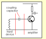
In the diagram below a capacitor connects a device
(sometimes called a TRANSDUCER) to a
transistor amplifier. The capacitor is called a COUPLING
DEVICE or COUPLING CAPACITOR as it couples the device to the
amplifier.
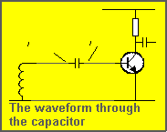
We have already mentioned how a capacitor works but in this
situation an even simpler explanation exists:
THE
COUPLING CAPACITOR
The capacitor works just like a magnetic window cleaner. A
magnet on a rag on the outside of a window can be moved up and
down by a magnet on the inside of the window.
In our case, any voltage appearing on the left side of the
capacitor "magically appears" on the right side. There
are coupling losses but these are minimal.
As mentioned above,
some input devices need rail voltage applied to them (or a
voltage lower than rail voltage) to produce
an output waveform, others produce a waveform when they are
struck or vibrated.
The end result is the same - a WAVEFORM.
But the problem is the SIZE OF THE WAVEFORM. Some device
produce a very large waveform while others produce a very small
waveform. If the waveform is very small, a very high gain
amplifier will be required.
In the common-emitter amplifier we will be describing, the gain
of a single stage is about 70 - 100. This may seem surprising
because if you refer to data sheets for most small-signal
transistors you find the DC gain is about 250 - 450. This is a
DC current gain. We are talking about a voltage gain.
When a transistor with a high current gain is placed
in a common-emitter circuit, the automatic biasing provided by
the base-bias resistor, produces a voltage gain of 70 - 100. We will
discuss the reason for this in a moment but it is very
technical. If you place the transistor in a pure DC circuit, you
will achieve a current gain of up to 450.
The fact is, you can only allow a voltage gain of 70 - 100 for the
stages we are describing. That's not really a problem as one
stage will provide 70x amplification and two stages will produce
70x70 = 4900x. We are talking about a voltage gain, so that if
the "device" produces 2mV output, the amplitude of the
signal after 2 stages will be nearly 10v. The only special value of voltage you
need to remember is 5v for digital circuits (the old style TTL
chips) and microcontroller projects. The voltage cannot be
higher than 5v. For a HIGH to be registered on one of the
input lines it must be about 70% of 5v = 3.5v.
To achieve this you will require two stages of amplification if the
"device" has a very low output. If the device has an
output of more than 70mV, a single stage of amplification will
be needed.
There is no general rule for the size of the output voltage of a
"pick-up device" however the table below is an approximate guide
and shows how each device is connected.
| DEVICE |
Circuit
Symbol & output capacitor |
Connect
to supply rail? |
Approx
output voltage |
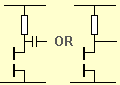
| Coil |

|
NO |
1mV to 100v!
It depends on the number of turns and the speed of the magnet |
| Photo transistor |
|
yes
|
1mV to 5v
depending on type of photo transistor |
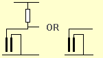
| reed switch |
|
yes
|
rail
voltage |
| ordinary switch |
|
yes
|
rail
voltage |
| touch switch |
|
yes
|
1mV to rail
voltage. Depends on the pressure of the finger and the
salt in the sweat on the finger. |
| Hall effect
device |
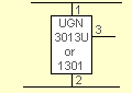
|
yes
|
rail
voltage if the Hall effect chip has an inbuilt amplifier |
| water
probes |
|
yes
|
1mV to rail
voltage. Depends on the size of the probes and the amount
of "salt" in the water. |
| electret microphone |
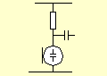
|
yes
|
1mV to
50mV depending on the audio level and the value of the
dropper resistor. |
| piezo diaphragm |

|
NO
|
1mV to
100mV depending on the "quality" of the
diaphragm and how hard it is "struck." |
| timing circuit |
|
yes
|
1mV to rail
voltage depending on the time when the voltage
detection is made. |
| solar cell |

|
NO
|
1mV to 450mV per
cell depending on the level of light. |
| Light-dependent
resistor (LDR) |

|
yes
|
1mV to approx
rail voltage |
| thermal sensor |
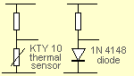
|
yes
|
1mV to rail
voltage. The voltage across an ordinary signal diode (1N
4148) increases by 2mV per degree Centigrade. |
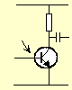
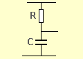
You will notice a
capacitor has been added to the reed switch, ordinary switch and
touch switch. These devices can be connected directly to the
rest of the circuit however the capacitor has an inbuilt
advantage.
When it is included, the closing of the switch sends a pulse
to the main circuit and if the switch remains closed, the
detecting circuit can still be used to detect other
switches.
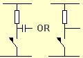
Some devices do
not need a capacitor and sometimes a capacitor cannot be
used. If the change in voltage is very SLOW, the increase or
decrease will not pass through the capacitor. The reason why the
signal passes through a capacitor is because the capacitor
does not have time to charge and thus the signal on one side
it passed to the other side. This is why the voltage
on one side can move up and down very quickly and the other side
responds with an identical movement.
Some devices do not
need a capacitor because they have a high impedance and
match the impedance of the amplifier PERFECTLY. An example is
the piezo diaphragm. It has a very high resistance (infinite)
and is effectively a piezo-electric capacitor.
Another device
not requiring an input capacitor is a set of water-level
probes. If the amplifier is a digital gate, (such as a
74c14 Schmitt Trigger) a pull-up resistor will be needed. If the
amplifier is a transistor, a pull-up resistor will not be needed
(the base-bias resistor acts as a pull-up resistor).
Now, the transistor amplifier:
There are a number of different common-emitter amplifier
circuits, but the simplest is shown below. Other arrangements
have better audio qualities but this is not necessary in our
case. We require high amplification and any distortion produced
by the stage is of no concern. The circuit consists of a
load resistor and base-bias resistor. The input and output
capacitors prevent any outside voltages influencing the voltage
on the stage. This stage is called an AC amplifier as it only
amplifies waveforms entering the stage via the input
capacitor.
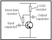
THE
SIMPLEST TRANSISTOR AMPLIFIER
The gain of the
stage will depend on the rail voltage. At 3v, the gain will be
about 50 - 70. At 12v the gain will be 100 or more.
The entire stage consists of only three components (a transistor,
and two resistors) and the resistors are chosen so that the
voltage on the collector is HALF RAIL VOLTAGE.
This allows the transistor to amplify both the positive and
negative portions of the incoming waveform.
How the transistor sits with the collector at half rail is quite
complex but it needs to be explained because the final collector
voltage depends on the
gain of the transistor as well as the value of the
resistors.
If you design a stage and the collector voltage is above or below
half-rail, the stage will not produce the maximum gain. You must
know how to bring a faulty stage to mid-rail
operation.
The design of the stage starts with the value of the LOAD
resistor. Its value is selected so that 1/10th milliamp
(100nanoamp) flows through the stage when it is fully and
correctly but no signal is being
processed. This is called the QUIESCENT current or IDLE
current. It si also called WASTED current as it is the current
that must flow all the time the circuit is turned on.
For 3v rail, the load resistor is 10k. For 6v rail the load
resistor is 22k and for 12v it is 47k.
Once the load resistor is selected, the base-bias resistor is
selected so that the collector voltage sits at approx mid-rail.
Experimentation has found this to be 1M for 3v, 2M2 for 6v and
4M7 for 12v. But these values correspond to a transistor
with a DC gain of 450.
If you have designed a stage and the collector voltage is BELOW mid-rail,
there are two things you can do:
1. Reduce the load resistor OR
2. Increase the base-bias resistor.
If the collector voltage is ABOVE mid-rail, the opposite
applies.
HOW
THE TRANSISTOR SITS AT MID-RAIL
This is the
technical part.
The transistor turns on and settles at mid-rail very quickly, so
we will have to take it very slowly:
When the power is first turned on, the transistor is not
conducting and the only things "in-circuit" are the
load resistor and base-bias resistor. Current flows through these
two resistors and turns on the transistor. The transistor is
like a variable resistor and when it turns on its resistance
decreases and forms a voltage divider with the load resistor.
This means the base-bias resistor sees a lower voltage being
supplied to it and thus a smaller current is passed to the
transistor.
The transistor keeps turning on but as it keeps turning on, the
base-current being supplied to it decreases. BUT the transistor
needs MORE current into the base to keep turning on HARDER and
HARDER.
So, an equilibrium point is very quickly reached where the
transistor cannot turn on any more because the base-bias
resistor cannot supply the required current. The result is the
transistor turns on with the collector at half-rail
potential. This is exactly what we want and is due to the
gain of the transistor, the value of the load resistor and the
value of the base-bias resistor.
CONNECTING
TWO STAGES TOGETHER
We mentioned above,
two stages of amplification are needed if the "input
device" has a very low output.
The simplest arrangement is to connect two common-emitter stages
together, separated with capacitors to keep the biasing of each
stage intact. The diagram below shows a two-stage amplifier:
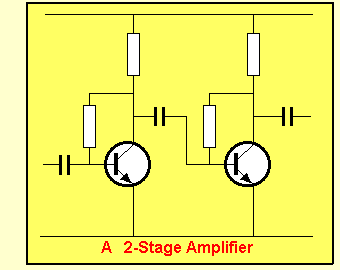
The two stage
amplifier above is called a pre-amplifier, high-gain amplifier
or 2-stage AC amplifier. It will only amplify AC
signals (waveforms).
This amplifier will suit the following input devices:
1. A coil - simply connect the coil to the input capacitor.
Suitable for frequencies above 100Hz.
2. A Photo transistor - suitable for frequencies above 100Hz.
3. An Electret microphone - frequencies above 100Hz.
4. A Piezo diaphragm - frequencies above 100Hz
5. A Light Dependent Resistor - suitable for frequencies above
100Hz.
Input devices that
can be connected directly to a Schmitt gate or microprocessor:
1. Reed Switch
2. Ordinary Switch
3. Hall effect device
4. Timing circuit
Input devices
needing additional "special" amplifying stage(s):
1. Touch Switch
2. Water probes
3. Solar cell
4. Thermal sensor
Interfacing these devices will be covered in a future section.
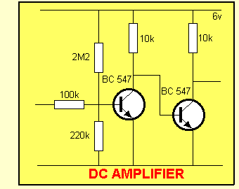
THE
DC AMPLIFIER
Devices with an
output voltage that changes over a long period of time
require a DC amplifier.
DC amplifiers are critical and difficult to design because they
do not contain capacitors to separate the stages. This means a
slightly incorrect voltage on the input will cause the collector
of the first transistor to be incorrect by approx 100x and the
second stage will amplify this another 100x or more! The result
will be a totally incorrect reading on the
output. A transistor in a DC circuit can exhibit a gain of
200x - 300x - or 400x. One of the biggest problems with a
DC circuit is the alteration of the "bias-point" (the operating point for each
of the transistors), as the temperature changes. Transistors
contain P-N junctions and as the temperature changes, the
voltage across the junction alters. This can change the current
in the first transistor and the second transistor amplifies the
change. The result is called an instability (thermal)
problem.
Forgetting thermal problems for the moment, the diagram below shows a typical DC amplifier. The first
transistor is biased OFF due to the 2M2 and 220k base-bias
resistors forming a voltage divider that puts 0.54v on the
base. This is below the "turn-on" voltage
required for a transistor. The result is the first transistor is
turned OFF and you can consider it to be
"out-of-circuit."
It is easy to see the second transistor is turned on via
the 10k resistor (on the base) and thus the output is LOW.
The circuit requires about 100mV rise on the input line for the
first transistor to turn on. The voltage between
collector and emitter drops to about 0.35v
and this is below that required by the second transistor to keep
it tunned on. The second transistor turns OFF and the output goes
HIGH.
The DC amplifier
above requires a relatively high voltage to turn on. You may
have only 1 or 2mV available (in the form of a rise and fall
voltage) and
require the amplifier to process the change. This requires a completely different circuit.
The diagram below will amplify very small signals. A standard 8
ohm speaker can be used as a microphone and the circuit
will provide a voltage gain of approx 1,000!
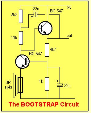
The main problem when designing a DC amplifier is the turn-on
voltage of the first transistor. The base must see about 650 -
700mV for it to be in a state where it can be turned ON more (or
less) when a slightly higher or
lower voltage is delivered.
This is a very difficult situation to achieve as the transistor
is thermally sensitive, the components are thermally sensitive
and the supply voltage must be absolutely stable. A slight
change in circuit current due to any of these components will be amplified by the
transistor and also by any other transistors in the amplifier. A
2-transistor stage can have an amplification of 1,000 or more so the front-end must be extremely stable.
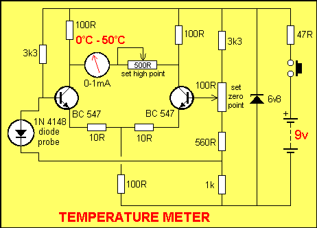
The diagram below shows a DC amplifier that amplifies the
voltage change across a diode. When a diode is heated, the
voltage across it changes at a rate of approx 2mV per degree
centigrade. This is amplified by the circuit and the result is
shown on
a 0 -1mA meter between the collectors of the two
transistors connected in differential mode. This type of circuit
has been selected to provide thermal compensation. Transistors
contain P-N junctions just like diodes and if the diode is
detecting temperature rise, the rest of the circuit may also be exposed to a temperature rise. By connecting the two transistors
in differential-mode, any temperature rise detected by one
transistor will cause the needle to move up scale. Any
temperature rise detected by the other transistor will cause the
needle to move down-scale. The result is the meter movement is
cancelled out when both transistors see the same temperature
rise. This leaves only the diode to influence the meter - very
clever!
The next page explains how the voltage changes on each
lead of a transistor - as the input rises.
NEXT
|