|
'508A
Details

Page 8
INDEX
The PIC12C508A is a low-cost 8-bit fully static, EPROM/ROM based CMOS
microcontroller. It employs a RISC (Reduced Instruction-set
Computer)
architecture with only 33 single-word single-cycle instructions.
All instructions are single-cycle (1uS) for a 4MHz internal RC oscillator,
except for program branches which take 2 cycles. The clock is internally
divided by four to produce one Machine Cycle. Instructions are executed in one
Machine Cycle. Instructions are 12-bit wide and the '508A contains 511 address
locations.
Four oscillator configurations are available.
1. The internal 4MHz RC oscillator,
2. External RC,
3. External Crystal/Resonator and
4. External Low power 32kHz crystal.
The '508 is only available in One-Time-Programmable (OTP) versions that are
suitable for production in any volume.
FEATURES
Only 33 single-word instructions.
All instructions are single cycle except program branches.
Operating speed: DC to 4MHz
12-bit wide instructions
8-bit wide data path
Seven Special Function hardware files 00h to 06h:
- INDF (Indirect File)
- TMR0 (Timer 0)
- PCL (Program Counter LOW bits)
- STATUS
- FSR (File Select Register)
- OSCCAL (Oscillator Calibration)
- GPIO (General Purpose In out lines) GP0, GP1, GP2, GP4, GP5. (GP3 is in
only.)
25 General Purpose Registers (files): 07h to 1F.
511 address locations for program: 000 to 1FE
Two-deep stack
Direct, indirect and relative addressing for data and instructions.
The ALU (Arithmetic Logic Unit) is 8-bits wide and capable of addition,
subtraction, shift and logical operations.
The W (working) register is an 8-bit working register. It accepts data
(called constants, literals or numbers) and transfers these values from one
file to another. It also performs logic operations but is not an
addressable register. (You cannot bit-test or shift the contents etc.)
Internal 4MHz RC oscillator with programmable calibration.
8-bit real time clock/counter (TMR0) with 8-bit programmable pre-scaler
Power-ON reset (POR)
Device Reset Timer (DRT)
Watchdog Timer (WDT) with its own on-chip RD oscillator for reliable
operation
Programmable code-protection
Power-saving SLEEP mode
Wake-up from SLEEP on pin change
Internal pull-ups on I/O lines
Internal pull-up on MCLR pin
Fully static design
Wide operating voltage: 2.5v to 5.5v
Low-power consumption: <<2mA @ 5v 4MHz 15uA @ 3v 32kHz
<<1uA standby
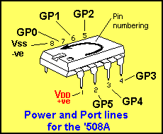
PIN DESCRIPTION:
Pin 1: VDD. Positive supply for chip and supply for I/O lines
Pin 2: GP5/Osc1/ClkIN. Bi-directional I/O line. Oscillator crystal
input. External clock source input. GPIO in internal RC mode only, Osc1 in all
other oscillator modes. Buffer type: TTL/Schmitt Trigger.
Pin 3: GP4/Osc2. Bi-directional I/O line. Oscillator crystal input. (XT
and LP modes only, GPIO in other modes). Buffer type: TTL.
Pin 4: GP3/MCLR/Vpp. Input line only. Master clear (reset) input.
Programming voltage (13v) input. When configured as MCLR, this pin is an active
LOW reset to the device. Voltage on MCLR/Vpp must not exceed VDD during normal
device operation. Can be software programmed for internal weak pull-up and
wake-up from SLEEP on pin change. Weak pull-up always ON if configured as MCLR.
Buffer type: TTL.
Pin 5. GP2/T0CKI. Bi-directional I/O line. Can be configured as T0CKI -
Timer0 clock timing. Buffer type: Schmitt Trigger.
Pin 6: GP1. Bi-directional I/O line. Serial programming data. Can be
software programmed for internal weak pull-up and wake-up from SLEEP on pin
change. This line is Schmitt Trigger input when used in serial programming mode. Buffer type: TTL/Schmitt Trigger.
Pin 7: GP0. Bi-directional I/O line. Serial programming clock. Can be
software programmed for internal weak pull-up and wake-up from SLEEP on pin
change. This line is Schmitt Trigger input when used in serial programming mode. Buffer type: TTL/Schmitt Trigger.
Pin 8: Ground reference for logic and I/O lines.
MEMORY ORGANISATION
PIC12C508A memory is organised into:
PROGRAM MEMORY and DATA MEMORY.
PROGRAM MEMORY
There are 511 PROGRAM MEMORY locations. This equates to a 511 instruction
program.
This is equivalent to 2 pages (a page is 000 to 0FF) or 0.5K of
memory.
RESET VECTOR
At 000 the programmer needs to place a value to tell the micro to GOTO an address that is the
start of the main program. For instance, the main routine may be at 1CF.
When you wake-up the chip from SLEEP, such as taking GP3 LOW, this will
cause a DEVICE RESET and the program counter will take the micro to location
1FF where it finds the instruction MOVLW XX - the oscillator calibration
instruction. After executing MOVLW XX, the Program Counter
will roll over to 000. At this address is placed an instruction such as GOTO
Main (Main will be at address 1CF).
CLOCK CALIBRATION VALUE
At 1FF is the clock calibration value. This value alters the frequency only
a very small amount and can be neglected, however location 1FF should not be
overwritten.
To keep the use of the '508A as simple as possible we will not be suggesting
the use of an external crystal (it takes up 2 lines if implemented!) - the
advantage of the '508A is the absence of external components such as oscillator
R's and C's.
ADDRESSING PROGRAM MEMORY
Program memory cannot be altered but can contain bytes of data in the form
of tables. Each byte of data must include the instruction RETLW. e.g:
RETLW 3A
RETLW 4C
RETLW BF
Tables must be in the first 0FF address locations (the first half of memory
for the '508A) as Direct Addressing instructions only allow the lower 8 bits of
the Program Counter to be addressed. See Direct Addressing in the Library
of Routines.
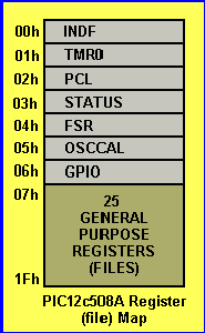
DATA MEMORY
DATA MEMORY has 32 registers or FILES.
The first 7 registers (00 to 06h) are SPECIAL FUNCTION REGISTERS and the
next twenty-five, (07h to 1F) are GENERAL PURPOSE REGISTERS. In our programs
the registers are called FILES to help you understand that data can be stored
in these locations.
The registers or FILES can be thought of as RAM. They are 8-bits wide.
Data is moved into or out of the files via the W (working) register.
Data can be shifted left or right and any bit can be TESTed, CLEARed or
SET.
No other data memory locations are available in the '508A, so you have to
remember that data storage is limited to about twenty bytes as some of the
files will be needed in the routines.
Data Memory can be addressed Directly, or Indirectly.
Direct addressing simply means to move data from a file (such as file 0C) to
the working register (W).
e.g: MOVF 0C,0
Indirect Addressing uses INDF and FSR registers. See Indirect Addressing in
the Library of Terms and Routines.
|
Address |
Name |
Bit 7 |
Bit 6 |
Bit 5 |
Bit 4 |
Bit 3 |
Bit 2 |
Bit 1 |
Bit 0 |
|
N/A |
TRIS |
I/O Control Register |
|
N/A |
OPTION |
Contains control bits to configure Timer0, Timer0/WDT prescaler,
interrupt on change and weak pull-ups |
|
00h |
INDF |
Uses contents of FSR to address data memory |
|
01h |
TMR0 |
8-bit real-time clock/counter |
|
02h |
PCL |
Low-order 8-bits of PC |
|
03h |
STATUS |
gpwuf |
|
PA0 |
TO |
PD |
Z |
DC |
C |
|
04h |
FSR |
Indirect data memory address pointer |
|
05h |
OSCCAL |
CAL7 |
CAL6 |
CAL5 |
CAL4 |
|
|
|
|
|
06h |
GPIO |
|
|
GP5 |
GP4 |
GP3 |
GP2 |
GP1 |
GP0 |
|
SPECIAL FUNCTION REGISTER SUMMARY |
|
R/W-0 |
R/W-0 |
R/W-0 |
R-1 |
R-1 |
R/W-x |
R/W-x |
R/W-x |
|
GPWUF |
|
PA0 |
TO |
PD |
Z |
DC |
C |
|
Bit 7 |
Bit 6 |
Bit 5 |
Bit 4 |
Bit 3 |
Bit 2 |
Bit 1 |
Bit 0 |
|
STATUS REGISTER
Address 03h
|
R = Readable bit
W = Writable bit
-0 = Value at Power On Reset
|
STATUS REGISTER (Address 03h)
This register contains the arithmetic status of the ALU (Arithmetic Logic
Unit), the RESET status and the page preselect bit for memories larger than 512
address locations (also called words - in this case a word is 12-bits
wide).
Bit 7: GPWUF: GPIO reset bit.
1 = Reset from wake-up from SLEEP on pin change.
0 = After power-up or other reset.
Bit 6: Unimplemented.
Bit 5: PA0. Program page preselect bits. For '508A = 0.
Bit 4: TO. Time-out bit.
1 = After power-up, CLRWDT instruction, or SLEEP.
0 = A WDT time-out occurred
Bit 3: PD Power-down bit.
1 = After power-up or by the CLRWDT instruction.
0 = By execution of SLEEP instruction
1 = The result of an arithmetic or logic operation is zero.
0 = The result of an arithmetic or logic operation is not zero.
Bit 1: DC Digit carry/borrow (for ADDWF and SUBWF instructions)
ADDWF
1 = A carry from the 4th low order bit of the result occurred
0 = A carry from the 4th low order bit of the result did not occur.
SUBWF
1 = A borrow from the 4th low order bit of the result did not occur.
0 = A borrow from the 4th low order bit of the result occurred.
Bit 0: C: Carry/borrow (for ADDWF, SUBWF and RRF, RLF instructions).
ADDWF
1 = A carry occurred
0 = A carry did not occur
SUBWF
1 = A borrow did not occur
0 = A borrow occurred
RRF or RLF
Load bit with LSB or MSB, respectively
OPTION REGISTER
(does not have an address)
The OPTION register is an 8-bit wide, write-only register containing various
control bits to configure the Timer0/WDT prescaler and Timer0.
|
W-1 |
W-1 |
W-1 |
W-1 |
W-1 |
W-1 |
W-1 |
W-1 |
|
GPWU |
GPPU |
T0CS |
T0SE |
PSA |
PS2 |
PS1 |
PS0 |
|
Bit 7 |
Bit 6 |
Bit 5 |
Bit 4 |
Bit 3 |
Bit 2 |
Bit 1 |
Bit 0 |
|
OPTION REGISTER
|
W = Writable bit
-0 = Value at Power On Reset
|
A RESET sets all the OPTION bits to "1."
TRIS overrides OPTION if GPPU is enabled and GPWU is disabled.
If TRIS bit is set to "0" the wake-up on change and pull-up
functions are disabled for that pin.
If the TOCS bit is set to "1" GP2 is forced to be at an input,
even if TRIS GP2 = "0."
Bit 7: GPWU: Enable wake-up on pin change (GP0, GP1, GP3).
1 = Disabled.
0 = Enabled.
Bit 6: GPPU: Enable weak pull-ups (GP0, GP1, GP3).
1 = Disabled.
0 = Enabled.
Bit 5: T0CS: Timer0 clock source select bit
1 = Transition on T0CKI pin.
0 = Transition on internal instruction cycle clock, Fosc/4.
Bit 4: T0SE: Timer0 source edge select bit.
1 = Increment on high to low transition on the T0CKI pin.
0 = Increment on low to high transition on the T0CKI pin.
Bit 3: PSA: Prescaler Assignment pin.
1 = Prescaler assigned to the WDT.
0 = Prescaler assigned to Timer0.
Bits 2-0 are: PS2, PS1 and PS0. These are the pre-scaler bits for Timer0 and
WDT as shown below:
|
Bit Value |
Timer0 Rate |
WDT Rate |
|
000 |
1:2 |
1:1 |
|
001 |
1:4 |
1:2 |
|
010 |
1:8 |
1:4 |
|
011 |
1:16 |
1:8 |
|
100 |
1:32 |
1:16 |
|
101 |
1:64 |
1:32 |
|
110 |
1:128 |
1:64 |
|
111 |
1:256 |
1:128 |
PROGRAM COUNTER
As a program instruction is executed, the Program Counter (PC) will contain
the address of the next instruction to be executed. The PC value is increased
by one every instruction cycle, unless an instruction changes the PC.
For the '508A, all the program is in page0. A page is 512 bytes. For the
'509, the program is in page0 and page1.
EFFECTS OF RESET
The Program Counter is SET to "1's" on RESET, which means the PC
addresses the last location in the last page i.e. the oscillator calibration
instruction. After executing MOVLW xx, the PC rolls over to location 00h and
begins executing user code.
The STATUS register page preselect bits are cleared on RESET and page0 is
selected.
On RESET, a GOTO instruction will automatically cause the program to jump to
page0 until the page bit is altered.
STACK
PIC12C508A,9 has a 12-bit wide push/pop stack. But most important it is only
2-HIGH. Thus only 2 consecutive CALL instructions can be accepted.
A CALL instruction will push the current value of stack1 into stack2 and
then push the current program counter value, incremented by one, into stack
level 1. If more than two sequential CALLs are executed, only the most
recent two RETURN addresses are stored. A RETLW instruction will pop the
contents of the stack level 1 into the program counter and then copy stack
level 2 into level 1. If more than 2 sequential RETLW's are executed, the stack
will be filled with the previously stored level2. Note that the W register will
be loaded with the literal value specified in the instruction.
INDIRECT DATA ADDRESSING
INDF and FSR Registers
The INDF register is not a physical register. Addressing INDF actually
addresses the register whose address is contained in the FSR register.
This is INDIRECT ADDRESSING.
See Indirect Addressing in Library of Routines for examples.
I/O PORT
As with any other register, the I/O register can be written and read under
program control. Read instructions (e.g MOVF, GPIO,W) always read the I/O pins
independent of the pin's input/output mode. On RESET, all I/O pins are defined
as input (inputs are Hi-impedance) since the I/O control registers are all set
to "1." GP0 and GP1 can be programmed in software with weak
pull-ups.
GPIO
GPIO is an 8-bit I/O register. Only the low 6 bits are used (GP0 to GP5).
Bits 6, 7 are unimplemented and read as "0's." Note: GP3 is INPUT
ONLY.
The configuration word can set several I/O's to alternate functions,
such as external oscillator, MCLR enabled. When acting as alternate functions,
the pins will read as "0" during port read. Pins GP0, GP1 and GP3 can
be configured with weak pull-ups and also with wake-up on change. These
functions are not pin selectable. If pin 4 is configured as MCLR, weak pull-ups
is always on and wake-up on change is not set.
TRIS REGISTER
The output driver control register is loaded with the contents of the W
register by executing the TRIS f instruction. A "1" on a TRIS
register bit puts the corresponding output driver in a hi-impedance mode. A
"0" puts the contents of the output data latch on the selected pins,
enabling the output buffer. The exceptions are GP3 which is only INPUT. Note: A
read of the port reads the pins, not the output data latches. That is: If an output driver on a pin is enabled, and driven
HIGH, but the external system is holding it LOW, a read of the pin will
indicate a LOW. The TRIS register is Write-only and is SET (output drivers
disabled) on RESET.
I/O INTERFACING
All port pins, except GP3 (which is input only) can be used for both input
and output. For input operations the pins are non-latching. Any input must be
present until read by an input instruction (e.g: BTFSS 06,0). The outputs
are latched and remain unchanged until the output latch is rewritten.
To use a port pin as output, the corresponding direction control bit in TRIS
must be cleared (= 0 = Output). For use as an input, the corresponding
TRIS bit must be set (= 1 = Input). Any I/O pin (except GP3) can be programmed
as input or output.
I/O PROGRAMMING CONSIDERATIONS
Some instructions operate as read followed by write operations. The BCF and
BSF instructions, for example, read the entire port into the CPU, execute the
bit operation and re-write the result. If you have two BCF instructions
following each other in a program such as BCF 06,5 BCF 06,4 the voltages on the
pins after the first instruction will still be settling when the second
instruction is being executed and a false reading will occur. To avoid this,
place a NOP between the instructions.
TIMER0 MODULE AND TMR0 REGISTER
The Timer0 module has the following features:
- 8-bit timer/counter register TMR0, readable and writable.
- 8-bit software programmable prescaler
- internal or external clock select
- edge select for external clock
Timer mode is selected by clearing the T0CS bit (OPTION<<5>>).
In timer mode, the timer0 module will increment every instruction cycle
(without prescaler). If TMR0 register is written, the increment is inhibited
for the following two cycles. The user can work around this by writing an
adjusted value to the TMR0 register. Counter mode is selected by setting the
T0CS bit (OPTION<<5>>). In this mode, Timer0 will increment either
on every rising or falling edge of pin T0CKI.
The T0SE bit (OPTION<<4>>) determines the source edge. Clearing
the T0SE bit selects the rising edge. The prescaler may be used by either the
Timer0 module or the Watchdog Timer, but not both. The prescaler assignment is
controlled in software by the control bit PSA (OPTION<<3>>).
Clearing the PSA bit will assign the prescaler to Timer0. The prescaler is not readable or writable. When the
prescaler is assigned to the Timer0 module, prescale values of 1:2, 1:4 . . .
1:256 are selectable.
USING TIMER0 WITH EXTERNAL CLOCK
When an external clock input is used for Timer0, it must meet certain
requirements. The external clock requirement is due to internal phase clock (Tosc)
synchronisation. Also, there is a delay in the actual incrementing of
Timer0 after synchronisation.
EXTERNAL CLOCK SYNCHRONISATION
When no prescaler is used, the external clock input is the same as the
prescaler output. The synchronisation of T0CKI with the internal phase clock is
accomplished by sampling the prescaler output on the second and fourth cycles
of the internal phase clocks (the oscillator is divided by four to produce a
machine clock cycle). Therefore it is necessary for T0CKI to be high for at
least 2Tosc (and a small RC delay of 20nS) and low for at least 2Tosc (and a
small RC delay of 20nS). When a prescaler is used, the external clock input is
divided by the asynchronous ripple counter-type prescaler so that the prescaler
output is symmetrical. For the external clock to meet the sampling
requirement, the ripple counter must be taken into account. Therefore it is necessary for
T0CKI to have a period of least 4Tosc (and a small RC delay of 40nS) divided by
the prescaler value. The only requirement on T0CKI high and low time is that
they do not violate the minimum pulse width requirement of 10nS.
TIMER0 INCREMENT DELAY
Since the prescaler output is synchronised with the internal clocks, there
is a small delay from the time the external clock edge occurs to the time when
Timer0 module is actually incremented.
OPTION REGISTER EFFECT ON GP2 TRIS
If the OPTION register is set to read TIMER0 from the pin, the port is
forced to an input regardless of the TRIS register setting.
PRESCALER
An 8-bit counter is available as a prescaler for the Timer0 module, or as a
postscaler for the Watchdog Timer (WDT). For simplicity, this counter is being
referred to as "prescaler." Note that the prescaler may be used by
either the Timer0 module or the WDT, but not both. Thus, a prescaler assignment
for the Timer0 module means that there is no prescaler for the WDT, and vice
versa.
The PSA and PS2:PS0 bits (OPTION <<3:0>>) determine prescaler
assignment and prescaler ratio.
When assigned to the Timer0 module, all instructions to the TMR0 register (e.g:
CLRF 01 MOVWF 01 BSF 01,x etc) will clear the prescaler. When assigned to WDT a
CLRWDT instruction will clear the prescaler along with the WDT. The prescaler
is neither readable of writable. On a RESET, the prescaler contains all
0's.
SWITCHING PRESCALER ASSIGNMENT
The prescaler assignment is fully under software control (it can be changed
during program execution). To avoid an unintended device RESET an instruction
sequence must be executed when changing the prescaler assignment from Timer0 to
the WDT. See data sheets from manufacturer for more details.
SPECIAL FEATURES OF THE CPU:
- Oscillator selection
- Power On Reset (POR)
- Device Reset Timer (DRT)
- Wake-up from SLEEP on pin change
- Watchdog Timer (WDT)
- SLEEP
- Code protection
- ID Locations
- In-circuit serial Programming
The PIC'508A has a Watchdog Timer that can be shut off only through
configuration bit WDTE. It runs off its own RC oscillator for added
reliability.
If using XT of LP options, there is always an 18mS delay provided by the
device reset timer (DRT), intended to keep the chip in reset until the crystal
oscillator is stable. If using INTRC or EXTRC, there is an 18mS delay only
on VDD power-up. With this timer on-chip, most applications need no external
reset circuitry. The SLEEP mode is designed to offer a very low current
power-down mode. The user can wake up from SLEEP through a change on input
pins or through a Watchdog Timer time-out. Several oscillator options are also
made available to allow the part to fit the application, including an internal
4MHz oscillator. The EXTRL RC oscillator option saves system cost while the LP
crystal option saves power. A set of configuration bits are used to select
various options.
CONFIGURATION BITS
The '508A configuration word consists of 5 bits. Configuration bits can be
programmed to select various device configurations. Two bits are for the
selection of the oscillator type, one bit is the Watchdog Timer enable bit
and one bit is the MCLR enable bit. One bit is the code protection bit.
OTP devices have the oscillator configuration programmed at the factory and
these parts are tested accordingly.
OSCILLATOR CONFIGURATIONS
The '508A can be operated in four different oscillator modes.
- LP: Low Power Crystal
- XT: Crystal/Resonator
- INTRC: Internal 4MHz Oscillator
- EXTRC: External Resistor/Capacitor
CRYSTAL OSCILLATOR/CERAMIC RESONATOR
In XT or LP modes, a crystal or ceramic resonator is connected to the
GP5/OSC1/CLKIN and GP4/OSC2 pins to establish oscillation. The oscillator
design requires the use of a parallel cut crystal.
When in XT or LP modes, the device can have an external clock source drive
the GP5/OSC1/CLKIN pin.
EXTERNAL CRYSTAL OSCILLATOR
Either a pre-packages oscillator or a simple oscillator circuit with TTL
gates can be used as an external crystal oscillator. Pre-packages arrangements
offer a wide operating range and better stability.
A well-designed crystal oscillator will provide good performance with TTL
gates. Two types of crystal oscillator circuits can be used: one with parallel
resonance, or one with series resonance.
EXTERNAL RC OSCILLATOR
For timing insensitive applications, the RC device option offers additional
savings. The RC oscillator frequency is a function of the supply voltage, the
resistor (Rext) and capacitor (Cext) and the operating temperature. In
addition, the oscillator frequency will very from unit to unit to parameter
variations.
The difference in frame capacitance between package types will also affect
the frequency.
For Rext below 2k2, the oscillator may stop completely. For values above 1M,
the oscillator becomes sensitive to noise, humidity and leakage. Rext should be
between 3k3 and 100k. Although the oscillator will operate with no external
capacitor, a value above 18p should be used for noise and stability
reasons.
INTERNAL 4MHz OSCILLATOR
The internal RC oscillator provides a fixed 4MHz (nominal) system clock. In
addition, a calibration instruction is programmed into the top of memory to
indicate the calibration value for the internal RC oscillator. This value
OSCCAL, is programmed as MOVLW xx where XX is the calibration value and is
placed at the reset vector. This will load the W register with the calibration
value upon reset and the PC will then roll over to 000. The user then has the option of
writing the value to the OSCCAL register 05, or ignoring it.
RESET
The device differentiates between various kinds of reset:
(a) Power On Reset (POR)
(b) MCLR reset during normal operation
(c) MCLR reset during SLEEP
(d) WDT time-out reset during normal operation
(e) WDT time-out during SLEEP
(f) Wake-up from SLEEP on pin change
Some registers are not reset in any way, they are unknown on POR and are
unchanged in any other reset. Most other register are reset to "reset
state" on power-on reset (POR), on MCLR or WDT reset during normal
operation. They are not affected by a WDT reset during SLEEP or MCLR reset
during SLEEP, since these resets are viewed as resumptions of normal operation.
The exceptions to this are TO PD and GPWUF bits. They are set or cleared
differently in different reset situations. These bits are used in software to
determine the nature of the reset.
MCLR ENABLE
This configuration bit when unprogrammed (left in the "1" state)
enables the external MCLR function. When programmed, the MCLR function is tied
to the internal VDD, and the pin is assigned to be a GPIO.
Power-On Reset (POR)
The PIC incorporates on-chip Power-On Reset (POR) circuitry which provides
an internal chip reset for most power-up situations. A Power-on Reset pulse is
generated on-chip when VDD rise is detected (in the range 1.5v to 2.1v).
To take advantage of the POR, tie the MCLR pin directly to VDD. An internal
weak pull-up resistor is implemented using a transistor. This will eliminate
external RC components usually needed to create power-on Reset. The Power-on
Reset circuit and the Device Reset Timer circuit are closely related. On
power-up, the reset latch is set and the DRT is reset. The DRT timer
begins counting once it detects MCLR to be high. After the time-out period,
which is typically 18mS, it will reset the reset latch and thus end the on-chip
reset signal.
DEVICE RESET TIMER
The DRT runs any time the device is powered up. DRT runs from reset only in
XT and LP modes. It is disabled from reset in INTRC and EXTRC modes.
The Device Reset Timer (DRT) provides a fixed 18mS nominal time-out on
reset. The DRT operates on an internal RC oscillator. The Processor is kept in
reset as long as the DRT is active. The DRT delay allows VDD to rise above VDD
minimum and the oscillator to stabilize. The DRT will also be triggered upon a
Watchdog Timer time-out (only in XT and LP modes). This is particularly
important for applications using the WDT to wake up from SLEEP mode
automatically.
WATCHDOG TIMER
The Watchdog Timer (WDT) is a free-running on-chip RC oscillator that does
not require any external components. It is separate from the external RC
oscillator of the GP5/OCS1/CLKIN pin and the internal 4MHz oscillator.
This means the WDT will run even if the clock on the GP5/OCS1/CLKIN and
GP4/OSC2 pins have been stopped, for example, by execution of a SLEEP
instruction. During
normal operation or SLEEP, a WDT reset or wake-up reset guarantees a device
reset. The TO bit (Status bit4) will be cleared upon a Watchdog Timer
reset.
The WDT can be permanently disabled by programming the configuration bit
WDTE as "0."
WDT PERIOD
The WDT has a normal time-out period of 18mS (with no prescaler). If a
longer time-out period is required, a prescaler with a division ratio of up to
1:128 can be assigned to the WDT (under software control) by writing to the
Option register. Thus a time-out period up to approx 2.3 seconds can be
realised. The CLRWDT instruction clears the WDT and the postscaler, if assigned
to the WDT and prevents it from timing out and generating a device reset.
The SLEEP instruction resets the WDT and the postscaler, if assigned to the
WDT. This gives the maximum SLEEP time before a WDT wake-up reset.
Time-Out Sequence, Power Down and Wake-Up from SLEEP Status Bits TO/PD/GPWUF.
The TO PD and GPWUF bits in the Status register can be tested to determine
if a RESET condition has been caused by a power-up condition, a MCLR or
Watchdog Timer (WDT) reset, or a MCLR or WDT reset.
RESET ON BROWN-OUT
A Brown-out is a condition where device power (VDD) dips below its minimum
value but not to zero and then recovers. The device should be reset in the
event of a brown-out. To reset the '508A when a brown-out occurs external
brown-out protection circuits are needed.
POWER-DOWN MODE (SLEEP)
A device may be powered down (SLEEP) and later powered up (Wake-up from
SLEEP).
SLEEP
The power-down mode is entered by executing a SLEEP instruction. If enabled,
the Watchdog timer will be cleared but keeps running, the TO bit (Status bit 4)
is set, the PD bit (Status bit 3) is cleared and the oscillator driver is
turned off. The
I/O ports maintain the status they had before the SLEEP instruction was
executed (driving HIGH, driving LOW or Hi-impedance).
It should be noted that a reset generated by a WDT time-out does not drive
the GP3/MCLR/Vpp pin low. For lowest current consumption while powered down,
the T0CKI input should be at VDD or VSS and the GP3/MCLR/ Vpp pin must be at a
logic high level if MCLR is enabled.
Wake-Up from SLEEP
The device can wake-up from SLEEP through one of the following events:
1. An external reset input on GP3/MCLR/Vpp pin.
2. A Watchdog Timer time-out reset (if WDT was enabled).
3. A change on input pin GP0, GP1 or GP3.
These events cause a device reset. The TO, PD and GPWUF bits can be used to
determine the cause of device reset. The TO bit is cleared if a WDT time-out
occurred (and caused wake-up). The PD bit, which is set on power-up, is cleared
when SLEEP is invoked. The GPWUF bit indicates a change in state while in
SLEEP at pins GP0, GP1 or GP3 (since the last time there was a file or bit
operation on GP port). Before entering SLEEP, read the input pins. When in
SLEEP, wake up occurs when the values at the pins change from the state they
were in at the last reading. If a wake-up on change occurs and the pins
are not read before re-entering SLEEP, a wake-up will occur immediately even if
no pins change while in SLEEP mode.
The WDT is cleared when the device wakes up from SLEEP, regardless of the
wake-up source.
PROGRAM VERIFICATION CODE PROTECTION
If the code protection bit has not been programmed, the on-chip program
memory can be read out for verification purposes.
ID LOCATIONS
Four memory locations are designated as ID locations where the user can
store checksum or other code-identification numbers. These locations are not
accessible during normal execution but are readable and writable during
program/verify.
Use only the lower 4 bits of the ID locations and always program the upper 8
bits as "1's."
PROGRAMMING THE '508A
The PIC12C508A is a One-Time-Programmable chip, so you must be satisfied
with the program you have written, before burning a chip. The '508A can be
serially programmed in a PIC programmer or while in the end application
circuit. This is done via five lines. One for clock, one for data, one for
power, ground and the programming voltage.
The PROGRAM MODE and VERIFY MODE is entered by holding pins GP0 and GP1 LOW
while raising MCLR from 0v to 13v. (The bar over the instruction:. . indicates
the pin is active when it is LOW). Once in this mode the user program memory
can be accessed and programmed in serial fashion.
The first selected memory location is the "fuses." This is
actually address FFF where the 5-bit configuration word is stored. The
configuration word holds the oscillator selection bits, the watchdog timer
enable bit, the code protection bit and the MCLR enable bit. GP0 and GP1 are
Schmitt trigger inputs in this mode. Incrementing the Program Counter once
(using the increment address command) selects location 000 of the program
memory.
NEXT
|