|
CRYSTAL LOCKED FM BUG |
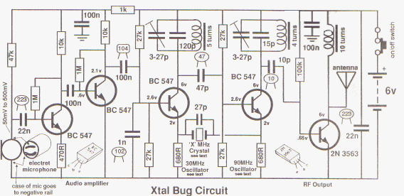
Xtal Bug Circuit
Producing a crystal locked transmitter is
a natural extension to our FM Bug series.
We have already produced a number of simple FM devices, (without the use
of a crystal) and showed how the power and frequency depends on a number
of factors including the voltage of the supply and the design of the
stages.
The broad term given to the oscillator stage of these transmitters is
"voltage dependent" as the frequency of the output is dependent on the
voltage of the supply.
We designed transmitters capable of transmitting 100 metres (the Ant),
400 metres (the Amoeba), 800 metres (the Voyager), 1km (the Ultima) and
others with ranges between 100 metres and 1km.
Even though these circuits were not crystal locked, they were extremely
stable, and could be made to transmit on the FM band or either above or
below it.
It was simply a matter of adjusting the spacing of the coil or the value
of the capacitor in the oscillator circuit to shift the frequency
anywhere on the band.
Once they were "set," the frequency remained surprisingly stable,
providing the supply voltage did not alter.
As the battery voltage fell at the end of its life, the frequency did
move slightly. Although this shift was very small, the change was
noticeable in some applications, such as long-term monitoring of alarms
etc.
|
features: |
|||
| Xtal (MHz) | 1st stage | 2nd Stage |
Output frequency |
|
10 |
x3 = 30MHz |
x3 |
90MHz 96MHz 96MHz |
In these cases it is important that the transmitter does not drift AT
ALL so that the link between transmitter and receiver can be maintained.
The only way to achieve this is to have an extremely stable oscillator -
one that is independent of the supply voltage. Designing such a circuit
is not an easy task and it has taken us quite a number of attempts to
get it to work properly. At last we have come up with a suitable design
and we have called it the Crystal Locked Bug - or Xtal Bug for short.
During our designing we had two major problems to overcome. One was
getting a low-cost crystal that would produce a frequency on the 88 -108
band and the other was getting good quality audio.
When audio is fed into a crystal locked oscillator, it must "pull and
push" the frequency of the oscillator - after all, that is why it is
called Frequency Modulation. In other words it must pull and push the
oscillator against the rigidity of the crystal and in doing so, the
audio gets distorted.
This is one of the major problems with a crystal oscillator and to solve
this we have placed the crystal in the emitter circuit. In this position
it allows the audio to be injected into the base of the oscillator stage
so that it can be combined with the 90MHz carrier (the carrier is the
frequency being produced by the stage) without being distorted.
Another problem was designing a crystal circuit at 88 - 108MHz. Crystals
are not capable of operating directly at this frequency. Most (cheap
ones) operate at about 8MHz to 10MHz. This is called their fundamental
frequency, if we want a transmitter to operate in the 88 -108 MHz band,
we need to use the crystal in its overtone mode.
In this mode a crystal with a fundamental frequency of say 10MHz can he
placed in a circuit that is designed to oscillate at a higher frequency
- say 30MHz. In other words the circuit components around the crystal
want to operate at 30MHz, the crystal merely keeps them operating at
EXACTLY this frequency.
In theory you could gel a 10MHz crystal to operate in a circuit at 90MHz
but the crystal would only be controlling the circuit every ninth cycle
and this is not providing a very tight control. It is much better to use
the crystal in one of its lower overtone modes, where the control is
much stronger. As the order of overtone increases, the crystal has less
"grip" on controlling the frequency. The most common overtone modes are
third (e.g. a 10MHz crystal operating in a 30MHz circuit) and fifth (a
10MHz crystal operating in a 50MHz circuit). We have decided to use the
crystal in its third overtone mode and provide a further stage, called a
tripler, to get the final required frequency of 90MHz.
THE CRYSTAL
The crystal we have used is a 10MHz device while the components in the
oscillator stage have been chosen so that the tuned circuit is operating
at 30MHz.
The way a crystal works is its capacitance changes abruptly at the
frequency marked on it.
The only problem with identifying the frequency of a crystal is some
crystals are marked with their third overtone value while others are
identified with their fundamental frequency, For instance. 27MHz
crystals for CB's, remote control cars and walkie talkies are generally
3rd overtone crystals and have a fundamental of about 9MHz while
computer crystals are generally identified by their fundamental
frequency.
Crystal circuits take advantage of the abrupt change in capacitance to
create a feedback path or alter the gain of the stage - as is the case
in our design.
In our circuit the crystal is placed between emitters of both stages and
has a 27p capacitor across it to increase its capacitance so that the
signal coming back from Q4 has a good, tight, control on Q3. The crystal
only likes to oscillate at a particular frequency (10MHz) and even
though Q4 excites it at 90MHz, it reacts once for each nine pulses and
sends a pulse to Q3 at the rate of 10MHz. The oscillator stage (made up
of Q3, 3-47p air trimmer, 120p ceramic and 6 turn coil on a ferrite
slug) is operating at 30MHz and it gets a pulse every third cycle to
keep it operating at exactly 30MHz.
The output of the 30MHz oscillator is connected to Q4 via a 47p
capacitor and the tuned circuit on the collector of CU is designed to
operate at 90MHz. This means a pulse from Q3 is appearing every third
cycle of Q4 to keep it operating at exactly 90MHz. In this way we have
achieved a crystal multiplication of 9 via two stages - one stage
operating in the third overtone mode of the crystal and the other
operating as a frequency tripler. The tripler is then buffered by an
output stage Q5 so that the loading effect of the antenna does not have
any effect on the operation of the tripler. The output stage also
provides a powerful output signal for the antenna.
A crystal locked transmitter also has the advantage that it can be worn
on the body or moved about without the frequency drifting.
As we have mentioned in a number of our previous articles, the human
body has an effect on any FM transmitter as it is 95% water and the
radio waves are readily absorbed. It's a bit like a bowl of water in a
microwave oven. The Radio Frequency energy from the magnetron is readily
absorbed by the water molecules in the bowl.
The same effect applies with radio waves from the antenna entering the
body. The human mass has a loading effect on the antenna and tends to
detune a normal voltage-controlled transmitter.
With a crystal locked device, frequency drift does not occur as the
crystal holds the frequency rigid, however the absorption effect cannot
be eliminated - the only solution is provide additional output power to
overcome it.
I had a discussion with Robert, a salesman from a company that sells
pendent transmitters from the USA. As you can expect, he did not
understand the effect of the body on this type of transmitter. He said
the body acted as a ground plane and improved the performance when it is
being worn. This is not true. The body only acts as a ground plane when
you are holding the grounded part of the circuit and leaving the antenna
free to radiate. But when you are near a transmitter such as a pendent
transmitter, the body actually absorbs the signal considerably as you
are not able to access the "earthy" part of the circuit.
While I am on this topic, the advertising for the pendent transmitter
claimed 100 metres. The sales department said they readily got 50 - 70
metres, but when I disputed these claims, they set one up and got 15 -
20 metres! So much for advertising!
We bought one of these for a customer but gave it back and went to our
workshop where Paul, the very same day, nutted out the problem of
transmitting and got our hand-held transmitter to go 100 metres through
walls and buildings! It will be the best transmitter you have ever seen
and will be presented very soon, so look out for it. Now back to the
topic:
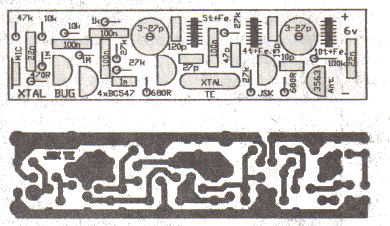
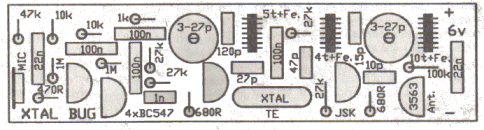
CONSTRUCTION
Before starting this project you should have a fair degree of skill in
assembly and soldering. After all. this is one of our more complex
designs and you should start with something simple if you want to get
the maximum understanding.
I don't want to go over the boring details of construction. I have
already covered them in previous articles.
For instance, I have already mentioned the fact that components should
be pushed up to the board before soldering to make the project look neat
and professional.
If you have not already built at least three of our simpler models, I
suggest you put together some of the following: The Ant, Gnat, Earwig,
Amoeba, Voyager, VOX and Ultima. Most of them can be found in our
publication "14 FM Bugs."
In all our projects, the position of each component is clearly marked on
the top of the board and you must know your resistor and capacitor codes
to identify them correctly.
When working with high frequency projects such as FM transmitters, it is
important to keep all the components as close to the board as possible.
The reason is two-fold. Firstly it looks neater and secondly the project
has been designed with everything placed tightly together and to get the
performance we claim, the components must match in size, shape and
position.
When working with 100MHz projects, the leads of any component become an
inductor and will change the characteristics of the circuit. This
applies to transistors, capacitors and coils if they are placed too high
above the board.
The same applies to making your own PC's or building the circuit on
matrix board etc.
Most constructors who build this type of project on Matrix board find it
does not work at all or has a very tow output. This is due to the leads
and tracks being longer than those on the printed circuit board. Long
leads become inductors and change the value and effectiveness of the
component - especially around the resonant circuits.
Sometimes the added length will prevent the circuit working altogether.
This is due to the gain of a particular stage being reduced to a point
where it is prevented from oscillating or amplifying.
It is not advisable to alter the layout in any way at all or substitute
other values unless you know exactly what you are doing.
The price of our kits and PC boards is so cheap that you won't save in
the long run. On the contrary. You can fall into a lot of traps. Simple
things like old-style ceramics can cause the circuit to be very noisy.
All our ceramics are NPO, meaning the capacitance is stable over a large
range of temperature. Old-style ceramics are not NPO types. In addition,
2% resistors can be very difficult to read and lead to the wrong value
being used. We use simple-to-read 5% values.
It is almost impossible for you to locate problems when they are
self-induced and the result is you will blame us for a bad design!
We have had it happen so many times. Some constructors build these
circuits with junk-box components (or components that appear to have the
correct value) and experience all sort of problems. They are constantly
ringing us for advise. It's only after a lot of wasted time on the phone
that they tell us they have used their own components!
This has led us to be very reluctant to give advice over the phone as we
cannot help you when other components have been used.
You must stick to what we say, and what we supply. That's why we supply
kits for everything we design and have been very successful in doing so.
The only new component in this project is the crystal. It is a simple,
non-polarised component that can be placed on the board, either way
around.
But you must be careful when soldering as the crystal element will not
like being overheated. Excess heat will damage the crystal structure and
you should not move the case once the leads have been soldered as this
can affect the mounting of the crystal inside the case.
FITTING THE
COMPONENTS
When fitting the components to the board, you can either start at one
end and fit each part as you come to it or start with the resistors,
then the capacitors, transistors and coils etc.
Each component should be pushed up to the board so that nothing is
higher than the resistors. The leads should then be spread apart
slightly so that the component stays in position during soldering.
It is best to add a few components at a time and splay the leads so that
the component doesn't fall out. The board is then turned over and placed
on a small piece of Blu Tack on the bench (so that it does not move),
while the leads are soldered.
Cut the leads near the board but don't cut into the solder joint as this
may create a fault.
Take at least two seconds while you are soldering each connection to
give the flux plenty of time to clean around the leads and make a good
connection. Too many constructors are frightened they will overheat the
component and they are not taking long enough. The result is the joint
is very rough in appearance and can very easily turn into a dry joint by
simply wiggling the lead.
You have to get to know the difference between soldering too quickly and
taking too long. This is the skill of soldering.
Make sure you do not forget any of the connections as you cannot
possibly expect the project to work if something has been missed.
Pay particular attention to the ends of the coils. They should be
cleaned with a knife, sandpaper or hot soldering iron and tinned so that
they will solder quickly when they are fitted to the board.
Don't forget, the microphone and transistors must be placed around the
correct way for them to work properly and these components are extremely
heat sensitive so don't take too long when soldering.
The 4 AAA cells are soldered together using short lengths of tinned
copper wire. This is cheapest and best method to create the 6v supply as
battery holders for AAA cells are no longer available.
HOW THE CIRCUIT
WORKS
Most of the description of how the circuit works has already been
covered in the introduction.
The only things left to discuss are the minor features like the 100n
capacitors across the power rails. These are designed to tighten up the
rails so that each of the stages work correctly without interfering with
each other.
This is especially important with the output stage as the transistor is
connected directly across the rails via a very low resistance coil.
The coil is only few turns of wire around a slug and appears to be
almost a short circuit as far as the transistor is concerned. But at the
frequency at which the circuit is operating, the coil becomes an
inductor in which a voltage is developed across the turns. The
characteristic of developing a voltage like this is one of the amazing
features of impedance and it is the generation of this voltage that
prevents excessive current flowing.
How this occurs is very complex and will be discussed in another article
but basically excessive current does not flow is because it takes time
for current to start to flow in an inductor and the transistor is only
turned on for a very short period of time (up to the time when the
maximum current just starts to flow).
The transistor then turns off and the current that was flowing in the
coil has produced magnetic flux. This magnetic flux now collapses and
produces a voltage across the turns of the coil. This voltage is of
opposite sign to the supply voltage and can be of a much higher
amplitude and since the transistor is
turned off, the only path for it; is to flow along the antenna lead.
I know you are going to say the antenna does not form a closed circuit
but when we are talking about high frequencies, energy is capable of
flowing along a lead and in doing so it produces radiation to the air,
called electromagnetic radiation or radio waves.
This converts energy from the circuit into a radiated signal.
The 100k resistor on the base of the output transistor is designed to
turn the transistor ON a small amount (about half) so that the signal
from the 10p capacitor can modulate the transistor (turn it on and off).
At 90MHz, the antenna lead appears to the output stage as a low
impedance load and energy from the coil will readily flow into it and be
converted to radiated signal as mentioned above.
This is how energy from the battery passes through the output stage to
the antenna.
THE 100n DECOUPLING CAPACITOR
We have mentioned in previous articles that all the tracks on a printed
circuit board appear as inductors to the various stages. As the
frequency of a stage increases, the length of the track has a greater
effect on its operation.
With a high frequency oscillator or output stage, long power rails have
a particularly adverse effect. It's like running the 240v power to a
caravan via a long lead. Every time a jug or radiator is turned on, the
lights will dim.
We can't tighten up the supply to the caravan but in a transmitter
circuit, capacitors are placed between the positive and negative rails
to tighten them up. These capacitors have only a very local effect and
must be placed very close to the components and stages they are
assisting.
That's why we need to have a number of capacitors across the power rail
as each is only effective for the nearby circuitry. These capacitors are
called decoupling capacitors and they prevent RF appearing on the rails
and upsetting nearby stages. The waveforms are absorbed by the capacitor
(as the capacitor takes a long time in relation to the duration of one
cycle) to charge up and discharge.
The 22n across the battery is also designed to tighten up the rails. The
output stage is effectively pulling the rails together and pushing them
apart while it produces the output waveform. If this were allowed to
happen, the output would be reduced in amplitude. It's a bit like
jumping up to touch the ceiling while standing on a mini-trampoline.
Your feet push down when you try to jump and the result is you rise very
little. The 22n
prevents this spreading and squeezing of the rails by taking a long time
to charge or discharge and thus keeps the rails tight and fixed.
The 100n capacitor and 1k resistor at the front end form a decoupling
network to prevent front-end instability called motor-boating. This
noise is due to the audio picked up by the microphone being amplified by
successive stages and appearing on the power rails as a low-frequency
waveform.
This waveform is then passed back to the front-end where it is once
again amplified. The result can be an uncontrolled whistle, or a
"putt-putt" sound similar to a motorboat.
The 1k resistor in combination with the 100n reduces the waveform
sufficiently so this feedback noise does not occur. In fact the
capacitor should be as large as possible and if 100n is not sufficient
it can be replaced with a tantalum of say 10u.
Removal of the microphone will alter the characteristics of the front
end and may cause motorboating to occur so don't remove it and expect
the front end to produce silence.
Instability in the front end can also be due to the microphone load
resistor being too low. Try increasing it if any form of instability is
detected.
IF IT DOESN'T WORK
If the project doesn't work, the first thing to do is check the
components for correct placement. The best thing to do is get someone
else to do this for you as you will not be able to check your own work.
Next check the soldering for faulty connections, especially around the
ends of the coils where the enamel will prevent the solder adhering to
the copper wire.
Then check the batteries for correct voltage and the continuity of the
switch. Do this by checking the voltage on the board when the switch is
turned on. Sometimes the switch can go faulty due to flux running up the
leads during soldering.
The circuit is very similar to some of the previous projects you have
made, such as the Amoeba, VOX and Ultima and you will find a lot of
helpful notes in these articles. The first transistor has a gain of
about 20 (it is the ratio of the 10k resistor/470R) and amplifies the
audio signals. The second transistor provides more gain to "drive" the
signal in to the oscillator stage.
It was necessary to have two audio stages to get sufficient audio gain
as you need a lot of "driving force" to pump the audio into the crystal
locked stages. The third transistor is a 30MHz oscillator while the
fourth and fifth transistors are operating at 90MHz.
To test this project you will need the peaking circuit and a
Field Strength Meter.
Firstly turn the project on and tune across the band to pick up a
signal. A feedback whistle will indicate the circuit is working. If no
signal is detected, the fault may be in a number of areas. To isolate
these areas, and "home in" on the fault, you will need the peaker. Place
it on the collector of the third transistor and you should get a
reading. If not, the oscillator is not working.
You can also check the collector of the 90MHz transistor as the output
of the 30MHz stage may be too low to get a good reading.
The 30MHz and 90MHz stages must be treated as a single unit when testing
them as the signal from the 30MHz stage passes through the 47p capacitor
and back to the 30MHz stage via the crystal and 27p capacitor.
The 30MHz oscillator stage is very similar to the oscillator circuits in
some of our previous projects, the only difference it is being injected
via the emitter to keep it "on frequency." You can check such things as
the 1n capacitor, emitter resistor, tank components and transistor by,
say, replacing them one at a time.
The air trimmers can very easily be damaged by excess heat. This is
indicated by them being difficult to turn.
You can then go to the 90MHz oscillator and tank components. Remove the
10p on the collector of the 90MHz transistor and fit the peaker to the
collector to detect an output.
Once you have a reading, replace the components and test the oscillator
before going to the output stage.
Remove the antenna and place the peaker on the "Ant."
(antenna) point. A low
reading may indicate the output transistor has been damaged during
soldering. If you are getting a blank spot on the
dial (a carrier) but no audio, the fault will lie in the audio stages or
electret microphone.
To test these you will need a small audio amplifier or CRO. These test
procedures have already been covered in previous articles, so get a copy
of "14 FM Bugs."
This concludes the testing section and the only thing left to do is
adjust the frequency of the resonant circuits to bring them in line with
the crystal frequency. This will also get the best output from the
transmitter.
PEAKING
Connect the peaker to the collector of the 30MHz stage and adjust the
air trimmer until the output is a maximum.
Next, place the peaker on the collector of the 90MHz tripler stage and
adjust the air trimmer until the output is a maximum.
You can now check the performance and frequency by connecting the
antenna and tuning in a digital radio to 90MHz. Keep the antenna wire
rolled up and place the transmitter some distance from the radio.
Take the radio down a few steps then up a few steps to see if the best
output is at exactly 90MHz. If this is the case, the project is
complete.
USING ANOTHER CRYSTAL
The output frequency of this project can be anywhere on the band. All
you have to do is fit the appropriate crystal.
Unfortunately there are not many low-cost, standard crystals that will
produce a frequency on the FM band however we have found four that can
be used. They are 10MHz, 12MHz, 16MHz and 24MHz. Other readily-available
crystals will give an output above or below the band and you will need
either a communications receiver or a detuned radio to pick them up.
It is an interesting exercise to try other crystals in the circuit as we
found a 12MHz crystal gave 96MHz. The first
stage operated at 48MHz and the second became a doubler to give 96MHz.
You can also use the 12MHz crystal in a third-overtone mode (36MHz) and
triple the next stage to get a 108MHz output, but 108MHz is slightly too
high for most digital radios.
If you are using a crystal other than 10MHz, the components in the first
oscillator stage will have to be changed to suit the new frequency. The
table below shows the value of capacitor we used for the various
crystals and the frequency at which the stage operated:
|
Crystal: |
Capacitor |
Frequency |
Coil |
|
10MHz |
120p |
30MHz |
5 turns |
|
12MHz |
180p |
48MHz |
5 turns |
|
16MHz |
180p |
48MHz |
5 turns |
|
24MHz |
180p |
48MHz |
5 turns |
The circuit we have presented is only one of the many ways to produce a
high frequency from a crystal. There ate lots of other ways, including
using the crystal in its third overtone mode and having two doubling
circuits to give 12 times the crystal frequency.
These are possibilities for later designs and we hope to bring some of
them to you in the near future.
CONCLUSION
The last thing to do is fit the project into a suitable plastic box.
There are a number of suitable types available from electronics shops or
alternatively a jewellery box or small chocolate box can be used. Quite
often you can buy a 10 carat diamond ring in a nice box for the same
price as a component box in an electronics store, so shop around - we
have found ideal boxes in the most unlikely of places. I cannot mention
where because this magazine is read by many young readers and we cannot
mention the word comdon.
PARTS LIST
1 - 470R (yellow-purple-brown)
2 - 680R {blue-grey-brown)
1 - 1k (brown-black-red)
2 - 10k (brown-black-orange)
4 - 27k (red-purple-orange)
1 - 47k (yellow-purple-orange)
1 - 100k (brown-black-yellow)
2 - 1M (brown-black-green)
2 - 3-27p air trimmer
1 - 10p ceramic
1 - 15p ceramic
1 - 27p ceramic
1 - 47p ceramic
1 - 120p ceramic
1 - 1n ceramic (102)
2 - 22n ceramics (223)
4 - 100n monoblock (monolithic) (104)
1 - 10MHz crystal (see text)
4 - BC 547 transistors
1 - 2N 3563 RF transistor
3 - 6mm x 2mm slugs F29 material
1 - 30cm enamelled wire .5mm dia
1 - 10crn tinned copper wire for cells
1 - electret microphone
1 - mini slide switch
4 - AAA cells
1 - 170cm antenna wire
1 - Xtal Bug PC BOARD
6/11/08