FIELD
STRENGTH METER Mk II
![]()
A Field Strength Meter is essential when designing and building transmitters.
It provides signal strength values and allows us to compare and estimate the
efficiency of a transmitter and its expected range.
|
SUMMARY |
|
|
Note: the pointer is not soldered to the trimmer
correctly. When the plates are fully disengaged, the pointer should
point to 75MHz.
Note: The bottom 3v lithium cell should be insulated from the holding wires
so that the cells do not "short-circuit." Put tape around the
bottom of each wire.
|
Field Strength Meter Mk II |
|
Field Strength Meter MkII circuit |
This project has 3 features.
1. It's a Field Strength Meter,
2. A Frequency Meter and,
3. An aid for testing detuned transmitters.
Its uses will become clear in a moment but firstly let's go over the background
of a Field Strength Meter.
A Field Strength Meter is essential when designing and building transmitters.
It provides signal strength values and allows us to compare and estimate the
efficiency of a transmitter and its expected range.
Obviously the most accurate way of getting these results is to make a field
test but this sometimes requires travelling long distances, so the next best
thing is to get results on the bench by using a piece of test equipment such as
an RF POWER METER.
An RF power meter is similar to a field strength meter, however the two are
used slightly differently.
An RF Power Meter is generally connected directly to the antenna of a
transmitter whereas a Field Strength Meter is placed NEAR the antenna without
physically touching it.
When you only have 5 - 50 milliwatts available, it is very difficult to place
a measuring device (such as a Power Meter) in the antenna circuit without it
absorbing and upsetting the energy being radiated.
When you are dealing with frequencies in the 100MHz range, the signal flows
over and through any device you place in the antenna circuit. Some of the
signal is absorbed in the measuring device so that the reading may not be a
true indication of the output. At the same time the performance of the
transmitter is reduced so you don't know how to interpret the results.
A much more accurate way of detecting the energy is to place a device NEAR the
radiating source (the antenna) so that it does not interfere with the
transmission.
This is the advantage of our FSM. It is placed near the radiating
source and detects the energy AT A DISTANCE so that the output is not upset.
This project differs from our Field Strength Meter MkI in that it is a
stand-alone unit and does not require connection to a multimeter.
It contains a set of 3 LEDs, wired in a staircase arrangement, so that they
light up progressively as the strength of the signal increases.
A trimmer capacitor at the front end tunes the exact frequency of the
transmission and as the FSM is brought closer to the antenna of the
transmitter, more LEDs will turn on.
We have already commented on the effectiveness of FM transmission in our many
transmitter articles and shown that the range is a result of good design. The
efficiency of a transmitter has a lot to do with the design of the output stage
and this can be improved by adding features such as a TANK CIRCUIT and a RADIO
FREQUENCY CHOKE. These are truly amazing additions as they increase the range
of the transmitter without consuming any more current because they concentrate
the signal into a narrow band.
One of the most-often asked questions is "How
much power is a particular transmitter producing?" This is very difficult to
answer but a simple rule of thumb is to allow 30% of consumption from the
supply as the output power.
One of our designs consumes 7mA @ 3v has an output of about 7 milliwatts.
Another design
has the same consumption and yet the range is only one quarter, so you can see
that efficiency plays a big part in getting the range.
Its output would be less than 1 milliwatt and this is shown by the fact that
the output is barely detectable on the LEDs.
The output difference between our highest and lowest transmitter is more than
100:1 and this has made it difficult for us to produce a project that will
cover the whole range.
To measure the output of the weakest transmitter you will have to wind up the antenna and push
the probe into the centre of the coil.
All the other transmitters have
sufficient output to detect the radiation when the antenna is outstretched.
With some of the transmitters, the tank circuit
must be adjusted so that the output is a maximum.
If you have a radio with a signal strength meter, you won't need this project,
but if you don't, it's what you need.
Most Field Strength Meters are designed for connection to transmitters with an
output of 1 to 1000 watts and are not capable of detecting outputs in the milliwatt range.
For low outputs we need a Field Strength Meter that will detect 1 - 50
milliwatts and that's why we designed this project.
As we have said, it is an adaptation of Field Strength Meter MkI and in place
of the meter in the output we have used a series of 3 LEDs. This makes it
self-contained and "frees-up" your multimeter for other uses.
The third feature mentioned in the introduction enables you to determine the
frequency of detuned transmitters. It is able to detect frequencies as
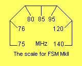
low as 75MHz.
This is very handy when designing transmitters for operation below the 88MHz
band.
When working with a transmitter in this range it is important to keep the
frequency just below 88MHz as many radios can only be detuned a few MHz before
the stations at the top of the dial start to appear at the bottom.
If a bug is below this limit it will be impossible to find, even on a detuned
radio.
There are two methods of detuning a radio.
One is to move the turns of the air coil near the tuning gang and see if the
stations move up or down the dial.
To produce a space at the bottom of the band, the stations must be moved up and
if you squash the turns too much, the top stations will wrap around and appear
at the bottom.
The other method is to adjust the trimmers on the back of the tuning gang. This
has proven to be the easiest and best method. Simply turn the trimmers until a
space is created at the bottom of the dial and your transmitter can be fitted
into the space thus created.
When you try to pick up the transmitter on a normal radio, it will be
invisible!
|
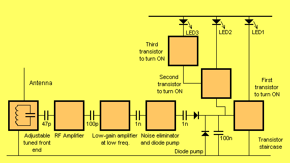
Field Strength Meter MkII block diagram |
HOW THE CIRCUIT WORKS
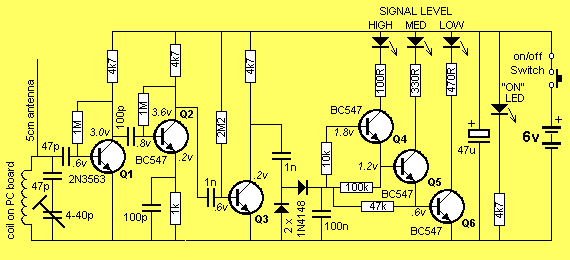
The circuit consists of a tuned front end, an RF amplifier, two further stages of amplification, a diode pump and a transistor staircase.
The circuit picks up RF energy on its 5cm antenna and passes it to a tuned circuit where all the frequencies, EXCEPT ONE are lost in the coil:capacitor combination. The only frequency to appear at the output (the top) of the tuned circuit is the one that is equal to the natural resonant frequency of the tuned circuit.
This signal is passed to the RF amplifier stage where it is amplified.
The coil for the tuned circuit has been etched on the PC board so that it is a known and fixed value of inductance. This allows us to use a trimmer capacitor and put a scale around it on the PC board so that you can read the frequency.
Even though the coil does not have a very good "Q" factor it will be ok in this case as the Q is not important.
In other words the tuning will be fairly broad and you will have to find the "centre spot" to get the exact frequency. Even then, the frequency will not be exact as the scale has not been individually calibrated. It's only designed to give you an approximate value.
Back to the tuned circuit:
The way in which the tuned circuit works is quite amazing. All the signals from radio stations, taxis, bugs, TV stations, cellular phones etc are picked up by the antenna and passed to the tuned circuit where they try to set it into operation.
It's a bit like hundreds of people trying to push a person on a swing - most of them will get in the way of each other. For example, a signal at 150MHz will try to push the swing when it is coming towards the pusher and the energy will be applied at the wrong time.
All the other signals will be pushing at the wrong time too and the only signal that pushes at exactly the correct instant will be the one marked on the scale. Its energy will not be lost in the tuned circuit but appear on the output. This signal is passed to the RF stage via a 47p capacitor for amplification.
The RF stage is able to amplify signals in the 100MHz range as we have used a high frequency transistor and the output appears at the collector.
Two further stages of amplification are needed to increase the signal so that it is large enough to be fed into a diode pump. Q2 is biased in a standard self-bias configuration while Q3 is biased in an unusual way. It is biased ON so that small signals on the input do not appear at the collector. This means the noise generated by the first two stages is prevented from appearing on the diode pump. Only signals above a certain threshold on the base of Q3 appear on the collector. This signal is rectified by a signal diode and fed into a 100n reservoir capacitor.
The other diode (between the 1n capacitor and negative rail) removes the negative portions of the waveform and thus discharges the 1n capacitor so that it can supply positive pulses for the charging process.
The first transistor in the staircase (Q4) starts to turn on when .6v is present on the reservoir capacitor. As the voltage rises to .65v the LED connected to the collector of 04 gets brighter and brighter. Due to the slight voltage drop across the 47k base bias resistor, the voltage on the reservoir capacitor needs to be slightly higher than .65v and once the first transistor in the staircase is turned on fully, the next transistor (Q5) will begin to turn on as the voltage on the reservoir capacitor (100n) rises slightly above 1.3v (.65v + .65v).
This process continues with the middle LED getting brighter and brighter until it is fully turned on.
As the voltage on the reservoir capacitor increases, the top LED will come ON and illuminate fully.
The 3 LEDs will give plenty of range as you can read values such as a LED fully turned on or partially turned on.
It is important to know that the lower transistor (Q4), turns on FIRST and as the voltage on the reservoir capacitor increases, Q5 then Q6 turns on. Without this, you will not be able to understand how the circuit works.
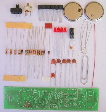
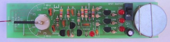
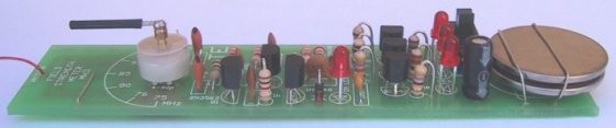
| Field Strength Meter Mk II Kit |
|
PARTS LIST |
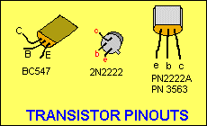
| 1 - 100R 1 - 330R 1 - 470R 1 - 1k 4 - 4k7 1 - 10k 1 - 47k 1 - 100k 2 - 1M 1 - 2M2 2 - 47p ceramics 2 - 100p ceramics 2 - 1n ceramics 1 - 100n mono-block capacitor 1 - 4 - 40p air trimmer 1 - 47u 16v PC mount electrolytic 2 - 1N 4148 diodes 5 - BC 547 transistors 1 - PN 3563 transistor 4 - 3mm red LEDs 1 - SPDT slide switch 1 - paper clip for pointer on trimmer 1 - 5cm enamelled wire for antenna 1 - 10cm tinned wire for batteries 2 - 3v lithium cells 1 - FSM MkIl PC board |
|
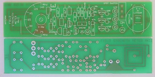
Field Strength Meter MkII PC board |
CONSTRUCTION
All the components fit on the board, with the two lithium cells at the end.
The overlay shows where the parts are placed and it's a simple matter to fit everything close to the board. If the leads of any of the components are left too long, the circuit will give a different gain to our prototype and not work properly, so keep everything neat.
The transistors, diodes and LEDs must be placed around the correct way and not overheated, otherwise the transistors will lose their gain and the LEDs will lose their brightness.
Bend the paper clip into an "L" shape. Do not cut it with side cutters as the metal is very hard and will damage your cutters.
The air trimmer (pointer) is now a ceramic air trimmer and the following photos show how it is soldered to the board and the the pointer soldered to the top when the air trimmer is turned so the moving vane is on top of the stationary vane. This position gives the air trimmer the maximum capacitance and now the pointer can be soldered as shown in the images.
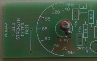
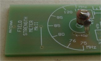
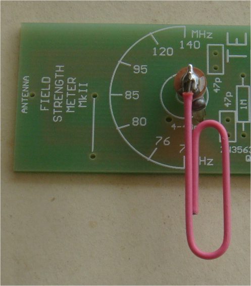
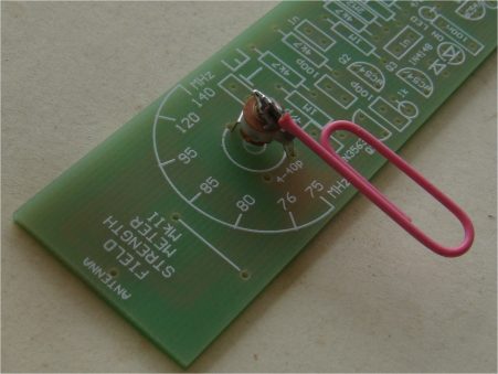
The pointer is now in
the correct position for the 75MHz frequency.
Don't forget the link at the front, near the etched coil.
Mark the ON position for the switch with nail polish and place electricians
tape around the two lithium cells before fitting them to the board, with straps
of tinned copper wire.
The rest of the assembly should be straight-forward.
IF IT DOESN'T WORK
The first thing to do is check the components against the overlay on the board.
All the parts must be around the right way and as close to the board as
possible so that everything will be the same as our prototype.
Check the underside of the board for any leads that are bent over and touching
other tracks.
Don't forget to check the soldering for shorts and make sure the tracks are not
damaged in any way.
Next check the current by measuring across the switch. In the quiescent state,
when only the power LED is illuminated, the circuit should consume about 3mA.
When 1 LED is illuminated, the circuit should consume about 10mA, for 2 LEDs
the circuit should take about 18mA and when the 3 LEDs are illuminated it
should be about 26mA.
If this is not the case, and the LEDs don't come on correctly, you will need to
look into the circuit more thoroughly.
The circuit can be separated into two sections at the point where the 1n
capacitor meets the two diodes.
The left half the diagram is classified as AC coupled and the right half is DC
coupled.
The letters AC, stand for "Alternating Current" however we really mean each
stage is CAPACITOR COUPLED so that the DC voltages on one stage are not
transferred to the next - a capacitor separates the stages.
The only thing that passes from one stage to the next in an AC coupled circuit
is the AC waveform and although you may think this can be called an ALTERNATING
CURRENT waveform, we do not use this term. We only say "AC coupled."
I know this is confusing however you have to learn the correct terminology if
you want to discuss electronics.
To repeat myself, we say the left-hand half of the circuit is AC coupled. We
don't say Alternating Current coupled. We just say "it's AC coupled" and only
the AC voltages are passed from one stage to the next.
In other words, each stage is self-contained and the biasing comes from within
the stage itself. If we view the waveforms on a CRO we call them AC waveforms
and yet they are really alternating voltage waveforms.
The right-hand half of the circuit is much easier to explain as it is DC
coupled (yes, Direct Current coupled). You can also say "Directly Coupled."
The easiest half to work on is the DC coupled section so we will start with it
and this means covering transistors Q4, Q5, Q6, and their associated
components.
The quickest way to check if this section is working is to take a jumper lead
from the join of the two diodes to the positive rail.
This will put full rail voltage on the reservoir capacitor and make all the
LEDs come on.
If this doesn't work, take the jumper lead from the collector of Q4 (the bottom
of the 470R) to the negative rail. This will turn on the lower LED. If not, the
LED may be around the wrong way.
Next, connect the bottom of the 330R to the negative rail (for the middle LED)
and finally the bottom of the 100R for the top LED.
This proves the 3 LEDs (and current limiting resistors) are working.
Shorting between the collector and emitter of the middle transistor (Q5) will
turn on the two lower LEDs and show that the lower transistor is functioning.
Shorting between the collector and emitter of the top transistor (Q6) will turn
on the 3 LEDs and show that the middle transistor is operating.
This is the extent of the simple DC tests for the staircase and the only other
thing you can do is take voltage readings on the base of each transistor when
the reservoir capacitor is fully charged. These values are shown on the circuit
diagram.
The 3 RF stages are much more difficult to test and the only thing you can do
is measure the voltage on the collector of each transistor and assume it is
biased correctly and the coupling capacitors are passing a waveform (the AC).
If you have a CR0 you can see the amplitude of the waveform increase as it
passes from one stage to the next and by bringing a bug such as a Voyager near
the antenna, the LEDs will gradually light up.
If you have a working model of
the FSM you can use it to test a non-working model. Use the antenna of the good
unit as a probe to see if a signal is being amplified through each stage of the
non-working model. If you don't have a FSM you will need something like a
100MHz CRO - but these cost between $1,000 - $4,000!
Now you can see why a FSM is so valuable. It's a very low-cost way of measuring
the characteristics of transmitters in the 100MHz range.
If you are building our transmitters, a Field Strength Meter is an essential
piece of equipment.
USING THE FIELD STRENGTH METER
We are assuming the project works correctly and has been checked as per the "If
it Doesn't Work Section."
To check the output of an FM transmitter, place it on the work-bench with the
antenna in a horizontal plane, away from any metal objects.
Switch it on and place the antenna of the Field Strength Meter about 20cm away,
with both antennas in the same plane.
Gradually turn the trimmer by moving the paper clip with your finger, while
keeping away from the coil on the underside of the board until the maximum
readout is detected on the LEDs.
The pointer will then give you the frequency at which the transmitter is
operating.
As you move the FSM away, the LEDs will dim and as it is brought closer, more
LEDs will come on.
If you wish to compare one transmitter with another, simply put the second in
exactly the same place on the bench with the antenna at the same distance. You
may have to re-tune the FSM to pick up the frequency; however you should get
the same reading on the LEDs if both have the same output.
When working with detuned transmitters, you can use the scale around the
trimmer to give readings from 75MHz.
If you have a transmitter tuned to a band above 108MHz, the FSM will detect
frequencies up to 140MHz.
When using the FSM, it is important to keep your hands away from the board,
especially the front end, as the loading of your body may affect the readings
slightly.
QUESTIONS FOR ADVANCED CONSTRUCTORS:
1. What is the purpose of the 47p in series with the 4 - 40p trimmer?
2. Why is the coil etched on the PC board?
3. What is the purpose of the 100p and 1k in the emitter of Q2?
4. Why is Q3 biased fully ON?
5. For the diode pump, does the transistor or the 4k7 collector resistor
charge the 100n?
ANSWERS:
1. The 47p in series with the trimmer adjusts the effective value of the
trimmer to 3p5 - 20p. The easy way to remember this is: two equal-value
capacitors in series produces a value of half the smaller value. Thus 40p and
40p produces 20p. For the smaller value, the ratio is about 10:1 or 4p:47p. We
use the same reasoning and see that the 47p will alter the 4p very little. This
is the way to see things without using mathematics.
2. The coil is etched or fixed on the board so that we can generate a
scale around the trimmer that will be the same for all models.
3. For low frequencies, (1 MHz etc) the 100p will have a high reactance and thus the gain of the stage will be the
ratio of the 4k7 to 1 k or about 5. Thus the stage will not amplify all the
hash and noise of the low frequencies.
4. Q4 is biased fully ON to further reduce the noise and hash produced
by a self-biased stage and also to give the diode pump full voltage swing.
5. The charging current for the diode pump is supplied by the 4k7. The
transistor merely pulls the 1n low to discharge it through the lower diode.