How A BD679
Works
![]()
In this issue we have designed a number of projects using a BD679 Darlington
transistor. This is a very handy transistor with very high gain and high
current handling capability. It is effectively two transistors in this one
package and can be used for many applications.
In this article we will cover this transistor and how to work with similar
super-alpha devices.
There are 4 ways to describe how a BD 679 works, they
are:
1. Using conventional current flow,
2. Using electron theory,
3. Using resistance analogy, and
4. Using the "visual" approach.
We will cover the 4 different ways and let you work out
which is the easiest to understand and how they interact with one-another.
Conventional current flow is easier to understand than
electron theory while the resistance approach is more closely allied to the
beginners level. But the visual approach is the best. By covering the 4
approaches, everyone will be able to understand the operation.
The author has used super-alpha (Darlington) devices for the past 20 years, when repairing TV's
and equipment, and studied the circuits to find out how they operate in each of
the applications.
The visual approach is easiest to understand is an NPN transistor with the emitter connected to the
negative rail. This is called a COMMON-EMITTER stage. But it works equally well with PNP transistors as you can
visualise them as being an upside-down NPN transistor.
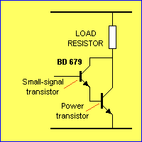
This is how to see it:
The BD 679 Darlington transistor is two transistors in one package, connected
as shown in the diagram above. The upper transistor is a small-signal
transistor and has its collector and base leads coming out of the package. The
lower transistor has its collector and emitter leads coming out of the package.
Obviously the collector lead is common to both transistors.
When a voltage is applied to the base of this Darlington
device, a current, flows into the base and turns the top transistor ON.
Delivering current into the base is exactly the same as lifting the base a small amount
with your finger. You don't need very much effort. The base is very easy to
lift. This small effort is amplified by the transistor to the emitter and it
lifts the emitter with the strength of about 100 times the effort you provided.
This "pulling-up" effect is now transferred to the base
of the power transistor and it is equivalent to raising the base with 100 times
more force than you exerted on the external base.
The power transistor inside the device PULLS DOWN very strongly on the bottom
of the LOAD RESISTOR and this allows a higher voltage to appear across the
LOAD. The result is the load is activated.
That's it. You lift the base UP very
gently and the Darlington transistor pulls DOWN very strongly on the load
resistor.
|
INSIDE THE BD 679 |
|
Inside the case of the BD 679 there are two transistors formed on a
single silicon substrate, plus two resistors and a protection diode. |
RESISTANCE ANALOGY
Now for the resistance analogy. When no current flows
into the base of the transistor, the resistance between the collector and
emitter leads is very high. When you allow a small current to enter the
base, the resistance between collector and emitter is reduced.
If you allow more current to pass into the base, the
resistance between collector and emitter becomes even lower. For example, when
no current flows into the base, the collector-emitter resistance may be 10Meg
ohms or more.
For a small current into the base, the collector-emitter
resistance may be 10k. When more current flows into the base, the
collector-emitter resistance may be 100 ohms or as low as a few ohms.
If we have a resistor - called the LOAD RESISTOR -
connect to the collector, we create a circuit similar to two resistors in
SERIES and current will flow through the load resistor and transistor according
to ohms law. As the resistance of the transistor decreases, the current through
the pair increases.
There is nothing special about this, it is simple ohms
law, as the transistor turns on harder, the current through the load resistor
(and the transistor) increases.
If the resistance of the transistor decreases to a few ohms, you can see the
current through the load will be a maximum and the device will be
activated.
CONVENTIONAL CURRENT APPROACH
The conventional current approach is the concept that
current flows out the positive terminal of a battery and into the negative
terminal.
In our case, when a small current flows into the base of
the Darlington transistor, the collector-emitter circuit allows a larger
current to flow.
When more current is allowed to flow into the base, the
transistor will allow a greater current to flow in the collector-emitter
circuit.
Since a load resistor is connected to the collector, this
collector-emitter current will also flow in the load.
THE ELECTRON APPROACH
The electron approach basically says that electron flow
occurs in the opposite direction to conventional current flow. In other words,
electrons flow out the base to the positive rail and others flow in the
emitter-collector circuit from the negative rail to the positive rail. The
electron approach is necessary if you want to describe the
actual operation of transistor itself.
THE VOLTAGE APPROACH
One final way of looking at the operation of the circuit
is the VOLTAGE approach.
The transistor does not turn on until a voltage of 0.65v + 0.65v = 1.3v
is supplied to the base lead.
This voltage allows a small current to flow into the base and the voltage on
the collector falls from rail voltage to slightly less than rail voltage. This
puts a small voltage across the load and a small current flows in the
load.
As the voltage on the base is increase a few more millivolts, more current is
able to flow into the base and the transistor multiplies this flow about 2,500
times and the increased current is allowed to flow in the collector-emitter
circuit.
Increasing the voltage on the base a few more millivolts will allow more
current to flow into the base (in the order of milliamps) and very soon the
maximum current will flow via the collector-emitter.
If the load is a relay or globe, the device will be activated.
You really need to combine all the concepts we have
described to see how the transistor works.
Once you can see how the collector and emitter leads
"squeeze" together or reduce in resistance, to deliver a current to the load,
you will be able to see how the transistor works.
As more current is delivered to the load, this will
introduce another feature you need to understand. It's called . . .
TRANSISTOR DISSIPATION
All the current through the load must flow through the
transistor - this is obvious as the two are connected in series, and when
current flows, heat is produced.
Unfortunately, transistors don't like to get hot and so
the heating effect must be kept to a minimum.
When the transistor is off (no base voltage
applied) no current flows and thus the heating effect is zero. This is
obvious.
This is one of the states of a transistor and is called
"cut-off" or simply "off."
As the transistor gets turned on, more current flows and
the heating effect increases.
Do you think this increase will be a maximum when the
transistor is fully turned on?
No! Amazingly, the heating effect increases until half
rail voltage appears on the collector and starts to reduce until it becomes
nearly zero when the transistor is fully turned on. This state is called
"saturation" or "bottoming."
This is a very important feature in electronics and means
there are two states when the transistor is dissipating the minimum energy
(heat) - the two states are: "bottoming" and "cut-off."
When a transistor is used in digital mode, it switches
from one state (say cut-off) to the other (saturation) very quickly and very
little heat is generated (lost) in the transistor.
But when a transistor is used in an audio application, it
moves very slowly between one state and the other and a lot of heat is
generated.
This heat must be passed to a heat-sink as quickly as
possible to prevent the transistor heating up and self-destructing.
Self destruction may be final or partial and may produce
loss of gain, an open circuit or a "short-circuit." Most often a transistor
goes short-circuit.
|
BD 679 RATINGS |
|
MAXIMUM RATINGS:
Collector-emitter voltage VCEO = 80v. The maximum voltage between collector and emitter when the transistor is NOT conducting. Collector-base voltage VCBO = 80v Collector current IC = 4amp. Maximum continuous collector current. Collector peak current (t = less than 1mS) = 7 amp. Base current IB = 100mA. The maximum current that can be fed into the base of the BD 679 without damaging the transistor. It is not the current required to turn it on fully - much less is required to turn it on fully. Junction temperature Tj = 150°C Total power dissipation 40 watts. This is the maximum wattage that can be dissipated by the transistor when it is adequately heat-sinked. Minimum forward current gain (hFE @1.5amp) = 750 Typical forward current gain (hFE @1.5amp) = 2500 Maximum forward current gain (hFE @1.5amp) = 3500 |
GETTING MORE TECHNICAL
Let's get a little more technical. One of the problems with the BD 679 is the minimum voltage between the collector-emitter terminals, when the transistor is fully turned on. This minimum voltage is about 2-3v, where as a normal transistor can go as low as .3v. For a MOSFET, the voltage can be .02v or lower.
Ideally, this voltage should be as low as possible as it determines the heat lost in the transistor when it is fully turned on. For instance, if a BD 679 is passing 4 amps in its saturated mode, the heat lost will be 2 x 4 = 8watts, or in the worst case, 3 x 4 = 12 watts.
For a MOSFET, the heat loss will be less than 0.08 watts.
WHY?
Why is the minimum collector-emitter voltage of a Darlinglon = 2.5v?
To see why, we need to see the diagram of the transistor
as shown in the figure below:
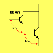
The small-signal part of the Darlington is riding on top
of the power transistor. As the collector of the power transistor falls during
turn-on conditions, it pulls the collector of the small-signal transistor down
with it and robs it of collector-emitter voltage.
This reduces the gain of the small-signal transistor and
the collector-emitter current is also reduced so the power transistor will not
be able to turn on as hard. This means the voltage on the collector will not
fall below 2.5 volts as this leaves only about 2.5v - .65v = 1.85v, for the
collector-emitter voltage of the small signal transistor.
This is just enough to give the transistor a collector
voltage so that it can provide some gain to drive the power transistor.
This is one of the limitations of a Darlington transistor.
BASE VOLTAGE
Another characteristic of a Darlington transistor is the
base voltage. It needs a voltage of 1.3v for the transistor to begin to turn
on.
This compares with .65v for a normal transistor.
Darlington transistors consist of two transistors in a
staircase arrangement and the base voltage is .65v + .65v = 1.3v. See diagram
below:

|
The two base-emitter voltages combine to produce 1.3v to turn the Darlington transistor ON. |
PNP DARLINGTON
By combining two PNP transistors, a PNP Darlington transistor can be created. This is shown below. Matched pairs of PNP and NPN Darlington transistors can also be obtained so that a push-pull output can be created.
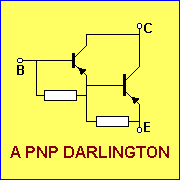
PHOTO DARLINGTON
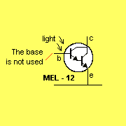
Other Darlington devices can also be created. A photo-Darlington transistor is available under the part number MEL-12. This is a
very sensitive device for detecting light and can be used for many applications
such as photo-electric beams, light detection etc.
The structure of the MEL-12 is shown below:
| MEL-12 Photo Darlington Transistor |
By building and experimenting with some of the projects we have described in this e-magazine you will get greater understanding of how a transistor works and how hot it can get before being damaged. To give an example, some of the first colour TV sets had the chrominance output transistors running so hot you could boil water on them. The latest sets use tiny plastic transistors and they run completely cold! It's all in the way the circuit is designed. Circuits should always be designed so that everything runs cold. That way, things last forever.
INSIDE DARLINGTON TRANSISTORS
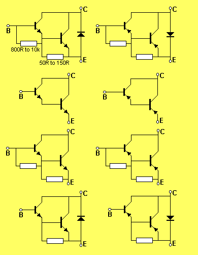
The transistors inside the Darlington package can be arranged in a number of different ways. Apart from the NPN and PNP devices, some have resistors in the package while others have no resistors. Some have a reverse protection diode between the collector and emitter terminals and others have protection diodes on the base. Below is a selection of the circuits inside Darlington packages.
The base resistors are designed to prevent the transistor "turning on" due to natural leakage through the small signal transistor.
These circuits show that Darlington transistors are not all the same and cannot always be replaced with a different type. The different value of base resistor will mean different base currents will be required and you should always replace a device with the same type.
![]()
