|
|

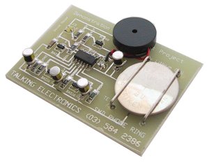
A DEMONSTRATION
SURFACE MOUNT PROJECT
It costs less than USD$11.00
![]()
![]()
This project has been specially designed to introduce you to SMD
(Surface Mount Devices).
Surface Mount is really not new. It started as far back as 1940 with
a hybrid circuit in a digital watch. A chip was cemented onto a slab
of ceramic material having gold tracks and film resistors. The LED
display was mounted in a similar fashion and the whole assembly
coated in epoxy to protect it before fitting into the watch case.
Surface Mount has come a long way since this simple beginning and
this project uses the latest components in a TELEPHONE RING
SIMULATOR. It has been laid out on a demonstration board to give you
plenty of room so you can fit the components by hand.
Normally, a circuit using SM would be too small and fiddly to build
by hand and couldn't be presented to beginners, but we have
attempted to make this project as simple as possible by spacing it
out and identifying the components so that almost anyone can put it
together.
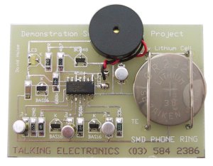
Complete Phone Ring project
See how the components are soldered to the board,
click
Although Surface Mount is rapidly gaining popularity with large
manufacturers, it has hardly made an entry in the hobbyist area.
The reason for this is two-fold. Surface mount components are
difficult to obtain at the best of times, especially in small
quantities, but more important, they are so tiny that manual
handling is almost impossible.
When you see them you will see what I mean. They are so small that
the slightest puff of wind will blow them off the workbench. If you
have poor eyesight, it may be out of the question, but for the rest
of us, it's a challenge worth investigating. To help you we have put
together a kit, and when you buy it you will appreciate the
features of surface mount and the problems we had putting the
project together.
The first problem we encountered was sourcing the components.
We contacted more than 15 suppliers who sell SM to get details of
price, size and availability. From the information we collected we
had to go to 5 of them to buy the parts.
Some had one item, others had a few more and all in all it was a
time-consuming exercise.
But the difficulty in locating the parts was not the only problem.
The variation in costs was also considerable. Some suppliers had low
prices but no stock while those with high prices had plenty of
stock. Isn't it always the way!
If we were in a position to buy large quantities, bulk prices would
have helped, but this is not possible when you are just starting out
and need small quantities.
The other factor controlling the price is the value of the
component. High value capacitors and electrolytics are considerably
more expensive than low values. To keep costs down, it is important
to be able to design a circuit around the cheapest components.
That's why we used 1u for the capacitors.
Now that we have done all the spadework, we want you to try Surface
Mount for yourself and put this project together.
When you do, you will learn how to identify, solder and handle these
tiny components and see why we say "Surface Mount has not been
designed for manual assembly."
The general purpose NPN transistor used in this project is a plastic SOT-23
type. It is marked 1K. (it is actually a BC 848B)
Here is the Philips range of BC 846,847 and 848 silicon planar epitaxial surface
mount transistors and the marking on the case:
| Marking | Vce Gain: | |
| BC 846A | 1A | 80v 125-500 |
| BC 846B | 1B | 80v 125-500 |
| BC 847A | 1E | 50v 125-900 |
| BC 847B | 1F | 50v 125-900 |
| BC 847C | 1G | 50v 125-900 |
| BC 848A | 1J | 30v 125-900 |
| BC 848B | 1K | 30v 125-900 |
| BC 848C | 1L | 30v 125 -900 |
Surface Mount has introduced a new range of case styles for diodes, transistors and chips. Here is a guide through the maze of new styles: SO means surface Mount. SOT is the case style for 3 or 4 leaded devices:
|
CASE STYLE |
MEANING |
| SOT 23 | 3-leaded package |
| SOT 143 | 4-leaded package |
| SO 8 | 8-pin Dual in Line package |
| SO14 | 14 pin DIL package |
| SO16 | 16 pin DIL package |
| also SO 24 and SO 28 | |
| PLCC 44 | 44 pin IC with 11 pins on each face |
| PLCC 68 | 68 pin IC with 17 pins on each face |
| PLCC 84 | 84 pin IC with 21 pins on each face |
THE SIZE OF SURFACE MOUNT
Surface mount is the transition between the components we know today
and those of tomorrow.
As far as designers are concerned, Surface Mount is only a
temporary, intermediate stage to assist in reducing the size of a
product to bring it on the market as soon as possible; while the
circuit is further developed and perfected.
The aim of a designer is to put all the circuitry into a single
custom-designed chip. But going from conventional componentry to
final design is often not possible in one step. Sometimes it
requires a few intermediate stages, requiring custom chips plus a
few discrete components. To do this, it is convenient to use surface
mount.
Products of tomorrow will be designed around a single dedicated chip
with only the need for batteries, switch and speaker etc.
We can see this already with calculators, watches, LCD games,
cameras and many more brilliantly designed products. They contain a
single dedicated chip and nothing more.
There are still a lot of other devices in the transitional stage and
these are currently using SM technology to reduce the size.
As the demand for a particular product increases, the cost of
re-designing the circuit (and the chip) becomes economical.
Eventually everything is incorporated into a single chip and the
evolution is complete.
This is the way surface mount is assisting designers to bring out
new products in steps and stages and as it gets phased out of one
design, another is taking on the transition.
It's difficult to know how long surface mount will be around, but
just like everything else, it will eventually be outmoded by a
radical new approach.
Until this time comes, there will be a demand for engineers to
design and work in this field and new openings are appearing all the
time. (Some surface-mount repair-work is also required in the
industry, but since this area of technology is so reliable, the demand is
very small. It mostly involves replacing mechanical components such as
switches and motors.)
We really shouldn't be presenting a "hands-on" project for Surface
Mount as it has been exclusively designed for robot handling, where
"pick and place" machines take components from carriers, spools,
hoppers, tubes etc and place them on a PC board with really amazing
speed and precision.
But if you intend to design projects in this medium, it's absolutely
essential to know how big the parts are, so that you can get some idea of
the space they occupy and how the board will turn out.
It's also essential to know how the devices are attached and the
process of soldering so you can design the board correctly.
Since normal surface-mount boards are Wave Soldered, it is important to place the
components at 90º to the action of the wave so they do not form
a shadow and prevent the solder from touching the pads.
This also applies to placing components in the shadow of taller
components, and there's 100 other tricks you have to learn.
So, if you want to start, here's your opportunity. There's nothing
like experiencing it first hand and if you put a kit together you
can at least say you have got off the ground.
SURFACE MOUNT ASSEMBLY
Since there are no leads on surface mount components, we do not need
any holes in the board (for multilayer boards, holes are required to
join one layer to the next - they are not for the components) and
the components can be loaded at impressive rates of something like
3600 devices per hour for a single head machine.
To prevent them dropping off the board before the soldering process,
tiny drops of glue are used and this keeps them firmly in position
so the boards can be turned up-side-down for wave-soldering.
Although Surface Mount devices are more expensive than conventional
components, the higher cost is offset by the savings in board space,
loading time and neatness of the final design.
This is where Surface Mount wins hands-down. A Surface Mount project
looks much smarter and more up-to-date than a conventional design.
The size of the board can be reduced by up to 50% and this makes it
very attractive for products that need to be compact such as
cameras, video machines, computers, and almost any other item you
can think of.
Some new chips are only available in Surface Mount and this forces
the manufacturers to take on the new technology.
This is exactly what happened to us. Our new speech chip (our
solid-state tape-recorder project) is only available in surface
mount and this forced us into the new technology. The same is
happening in design laboratories all around the world and in fact,
SM is seeing a growth rate of 15% per year with much of the new
growth taking place in the high volume, high-technology area.
The range of components is increasing too and already we have
Surface Mount coils, inductors, transformers, and other devices you
never thought could be produced in such minûte form. There is no
limit to the ingenuity of engineers. Eventually standard components
will be taken over completely and although this may take a number of
years it will certainly occur. We have already seen the demise of
the valve, the 1 watt resistor and many other components. It's only
when I see them in a museum that I marvel at the leaps we have made
in technology.
If you think this won't happen to conventional componentry, you are
kidding yourself. These changes are as certain as progress itself.
They are driven by economics and economics runs the world.
Surface Mount has arrived and is here to stay. Manufacturers can see
the savings in this area and are setting the pace.
And, believe me, the pace is mind blowing. Apart from
miniaturisation brought about by surface mount, we have large scale
integration and multi-layer PC boards. These have combined to shrink
devices from desk-top size to palm size - with 10 times the features
and 100 times the power!
Manufacturers of VCR's, TV's, automotive instruments, cameras,
computers and TOYS have all opted for surface mount as their
preferred form of construction.
Why have we included toys? Because toys represent one of the
greatest driving forces in the electronics industry. Many of the
recent advancements in electronics have taken place through the
medium of toys.
Talking dolls, whistling keychains, swearing keyrings, etc, have all
introduced the "dob of electronics."
If you have ever taken a whistling or talking keyring apart, you
will find it contains a single chip mounted directly on the PC board
and covered with a dob of potting compound. Some of the earlier
designs used discrete chips and a few resistors but as the designs
were tidied up, this was converted to the "dob of potting compound."
This is commonly called COB (Chip On Board).
The reason why manufacturers use toys as the proving ground is quite
simple. It provides a huge market that can be supplied and tested in
a very short space of time. This means the designers get rapid
feedback and the product can be updated and perfected very quickly.
Speech chips have followed this trend. Early chips cost more than
$70 each while the latest are surface mount and cost less than $10!
You can buy 30 seconds of digitised speech on a keychain or in a
credit card for less than $8!
The main problems with early
chips was understanding the robotised speech. It was difficult to
work out what was being said. But the new chips are so clear that
you think it's a tape recording.
HANDLING SURFACE MOUNT
You won't believe anything I say about the size of these components
until you see them for yourself.
The size is totally unbelievable and it may take a while to build up
enough courage to take them out of their carrier strips.
Normally these devices are not handled by humans and it was never
intended for them to be touched at all. The fact that some
components have values marked on them is merely a result of pressure
from end-users.
There is no real need to have any markings on them as they are
handled from start to finish by computer controlled insertion
equipment.
Even testing and alignment of the built-up board can be carried out
by robot testers and so component marking is a bonus for us.
A very small percentage of surface mount devices are soldered by
hand in short-run productions and in these cases the operator works
under a low magnification lenses or with the naked eye. To do this
sort of work you need to have very good eyesight, nimble fingers and
a calm temperament.
Once the initial shock of the size subsides, you can get down to
organising your soldering equipment and see if you are going to be
able to physically handle the task. You may need tweezers to pick up
the parts and something to hold them in place while soldering.
To do this properly you really need three hands but if this is not
available, you will have to use some other means of holding the part
while feeding the solder and using the iron.
If you have someone that can help you, now is the time to enlist
their assistance. I'm not going to discuss the need to be an expert
at soldering as the sheer size of the components will keep any
absolute beginner away.
However I am going to say that you can forget the cheap and rugged
40 watt soldering iron, the instant heat iron and many of the other
so-called electronic soldering irons such as the gas iron, soldering
gun and even the 700°F soldering station. They are all far too hot
and/or too cumbersome for this type of work. You need a soldering
iron or station with a temperature of 320°C to 350°C and a very fine
tip. When I say fine, I mean a tip that will almost prick you if you
touch it.
This fineness is absolutely essential for soldering the pins of the
IC as the lead spacing is half that of conventional IC's. Some of
the other components can be soldered with a medium tip, but
certainly not the IC.
We will not be gluing the components to the board before soldering
as the glue is very expensive and has a life of only a few months.
Instead we will be holding each item in place with a probe (such as
a paper clip or fine screwdriver) while tacking it in place, prior
to soldering.
This is where you can ask for assistance by getting someone to hold
the component or add the solder while you solder it in place.
Some components, such as ceramic capacitors, are not identified in
any way while those that are marked, (the resistors) require a magnifying glass to
read the numbers.
We have placed the components in a carrier strip in the kit and
enclosed a note to let you know how they are arranged. Do not take
any of them out of the strips before they are required as you will
not be able to identify them if they are mixed up. The old motto
"look but don't touch" certainly applies.
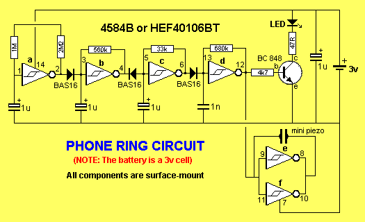
As we said in the introduction, this project is a TELEPHONE RING
CIRCUIT using a mini piezo as the output device and a CMOS Schmitt
trigger as the oscillator and driver.
One of the outputs of the chip also drives a LED via a transistor
and this has been done to add a transistor to the board.
Some constructors will say the chip is the hardest component to fit
while others will have enormous difficulty with the transistor.
In fact, this project would be ideal as a soldering test for
advanced students as it will not only test soldering skills but also
neatness, placement of parts and identification.
I believe a similar project was passed around a group of 20 workers
at a hi-tech plant with the requirement to desolder all the
components from the model and solder them back in place.
I understand that all the components withstood 20 solder and
desolder operations without a failure.
The fact is, surface mount components are extremely robust if
soldered quickly at the correct temperature. They are designed to
withstand a 10 second submersion in molten solder or other fluid,
but if you subject them to a higher temperature, you run the risk of
premature and permanent damage.
ASSEMBLY and SOLDERING in INDUSTRY
There are three types of Surface Mount assembly. The first is
placement of surface mount components to one or both sides of the
board. The second has both surface and through-hole components on
one or both sides. The third type has through-hole components on the
top side and surface mount components on the bottom.
The different loading techniques for these boards calls for
different soldering methods and the most common methods are: Reflow
and Wave.
In the Reflow method, solder is screened onto the pads in a printing
operation or individually added by means of a gun. The trackwork has
been previously protected with a mask to prevent solder creating
shorts and bridges. The components are then added and kept in place
with solder paste or tiny dobs of non-conductive glue.
The boards are then passed through an infra-red or convection oven
that allows the solder to melt.
Another method of reflow is to immerse the board in a saturated
vapour of a boiling Fluorinert liquid.
The vapour, at the temperature of the boiling liquid, gives up its
heat, causing the solder to flow. In the wave
soldering process, the board is dipped in flux and placed up-side
down over a bath of molten solder. A wave of solder is created that
rises up to touch the board and complete the soldering process.
These processes sound very simple but in fact involve a high degree
of technical skill. For instance, if a reasonably complex board has
100 faulty joints per million, the yield is almost zero and nearly every
board has a faulty connection!
With surface mount, the soldering process not only has to provide
good electrical connection but since the leads do not go though
holes, it has to provide good mechanical connection too.
The design of a surface mount board becomes much more critical than
a through-hole board due to the size of the components, the size of
the lands, the placement of the components and the consideration
given to heat stress both during and after soldering.
This is an entire subject on its own and technical centers can be
contacted for more information for those who want to be involved in
this area.
Along with the different soldering processes there are a range of
soldering faults, where the components have either dropped off the
board or begun to stand up due to a number of problems. The most
common fault is called "tomb-stoning" where capacitors, resistors and
packages stand on end after soldering. This results from improper
pad design, unequal solder mass, shadowing of the component,
misplacement of components, poor quality solder paste and wrong
soldering temperature. Fortunately, we won’t have any of these
problems in this project as everything will be soldered by hand.
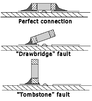
Some of the faults due to soldering, insufficient glue
and other factors
An enlarged view of the board showing where the components are
located.
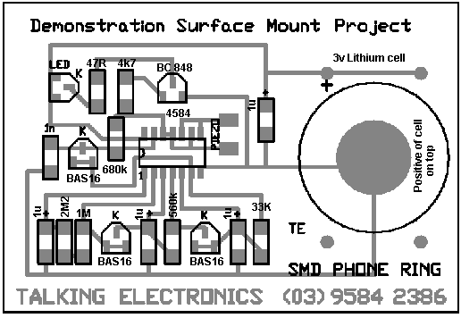
HOW THE CIRCUIT WORKS
The circuit consists of 6 building blocks and the first is the inverter between pins 1 and 2. This forms a low frequency oscillator with a 1u and 1M + 2M2 resistor. It governs the overall timing of the ring by creating an ON and OFF time. When the output is LOW, the tone is emitted from the piezo. When the output is HIGH, the tone is inhibited and this produces the silence between the rings.
This oscillator has an equal mark-space ratio to give the "rings" the same length of time as the silence.
The second oscillator operates at about twice the frequency of the first (this can be seen by the different value of the resistors as both capacitors have the same value).
The frequency has been adjusted so that it produces two highs during the interval when it is activated. The second oscillator does not produce two full cycles but only one and a half as it is the HIGHs that are required.
During each of these HIGHs, the third and fourth oscillators produce a warble that simulates the 33Hz ring of the "bell." The third oscillator generates the 33Hz frequency and this gates the fourth oscillator to produce a 1kHz tone for the piezo.
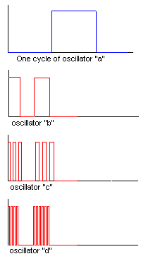 |
| Oscillator "a" (made up of the gate between pins 1 and 2 provides the overall ON/OFF timing for the ring. When it is HIGH, oscillator (b) produces two HIGH's. Oscillator (c) produces about 10 high's for each HIGH of oscillator (b) and oscillator (d) produces about 40 HIGH's for each HIGH of oscillator (c) to give the characteristic phone-ring. |
The output of this oscillator drives the base of the buffer
transistor and also one side of the piezo. The other side of the
piezo is connected to the output of two buffers in parallel and this
provides good pull-down capability when the left side of the piezo
is high.
The only fault in the design of this circuit is the drive to the
left-hand side of the piezo. We should have included driving buffers
to give it the maximum swing and thus the maximum output. But since
we did not have any left over, this is the best we could do.
When the piezo is driven from a pair of buffers on each side, it
sees a voltage swing of nearly twice the rail voltage and this gives
it the highest output.
The tone is also passed to a LED via a transistor to give a visual
indication of the operation of the circuit.
A 47R resistor has been included in series with the LED to limit the
current. It is essential to include a resistor as the LED drops a
fixed voltage (called the characteristic voltage drop) when it is
illuminated and the transistor drops a fixed voltage across the
collector-emitter terminals when it is turned on.
The voltage drops are 1 .7v for the LED and .5v for the transistor.
This adds up to 2.3v and thus we must include a resistor to drop .7v
from the 3v supply rail. By making the resistor 47R we allow a
maximum of 1.4mA to flow.
Without this resistor the power rails would be pulled down to 2.3v
every time the LED is turned on.
This would cause (a) a very high current to flow through the LED and
(b) faulty operation of the circuit as the power rails fluctuate.
The 1u electrolytic across the power rails reduces the impedance of
the battery and provides uniform rail impedance during the life of
the battery.
A lithium battery has been used as it produces 3v so that we only
need a single cell to provide the minimum voltage for the chip.
Between each of the oscillators is a diode called a gating diode. Its function is to turn the oscillator on and off when required. Here is how it works. We will use the second oscillator as an example, as shown in the figure below.
When the first oscillator (between pins 1 and 2) is HIGH, it is equivalent to connecting the anode end of the diode to the positive rail and this will have the effect of charging the electrolytic. The diode will be able to supply more current to the electrolytic than can be bled away by the 560k resistor and thus the capacitor remains charged. This means the inverter (between pins 3 and 4) will not change state and it is thus 'jammed."
When the first oscillator goes LOW, the diode is effectively connected to the negative rail and ceases to have any effect on the second oscillator.
By turning the diode around the other way, the oscillator will be blocked or jammed by a LOW from the previous oscillator as the diode will bleed away any charging current so that the capacitor will not rise higher than about .6v.
This is a very handy way of gating or controlling an oscillator by the use of diodes.
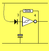
An oscillator jammed" by a gating diode.
A HIGH on the diode prevents the oscillator working.
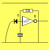
An oscillator jammed" by a gating diode.
A LOW on the diode
prevents the oscillator working
|
PARTS LIST |
| All components are surface mount Resistors 1 - 47R (marked 470) 1 - 4k7 (marked 472) 1 - 33k (marked 333) 1 - 560k (marked 564) 1 - 680k (marked 684) 1 - 1M (marked 105) 1 - 2M2 (marked 225) Capacitors 1 - 1n ceramic (102) 4 - 1u electrolytics Semiconductors 5 - BAS16 signal diodes (A6) 1 - BC 848B transistor (1K) 1 - surface-mount LED 1 - 4584B Hex Schmitt Trigger (HEF40106BT) Miscellaneous 1 - mini piezo 1 - 3v lithium cell type CR2032 10cm tinned copper wire 20cm very fine solder 1 - paper clip for holding parts 1 - Phone Ring PC board |
CONSTRUCTION
The object of this project is not to rush, but take it slowly and
produce a neat result.
Start by creating a clear space on the workbench and get all the
necessary tools and equipment ready. Make sure all the parts are in
the kit by checking it against the parts list and lay everything out
neatly in readiness. Look at the carrier strips so that you know
what’s inside. Clean the tip of your soldering iron on a wet sponge
and open out the paper clip supplied in the kit to form a probe to
hold the parts during soldering.
Take a little time to look at the legend on the board for the
position of each part and also refer to the circuit diagram and
isometric to see where everything goes. Make sure you know where
each of the parts is to be placed before starting as it will be very
difficult to remove something once it is soldered in place.
Some of the parts are not identified so don't remove anything from
the carrier strips until they are needed.
There are two methods of construction. You can start at one end of
the board and fit each part as you come to it or take one component
at a time from the carrier strips and solder it in place.
It does not matter which method you adopt, however I suggest you fit
the IC first. We have not included a socket for the chip as it is
more expensive than the chip itself and they are rarely used in any
case - so you will have to be extremely careful, not to damage it.
Firstly position the chip on the board so that pin 1 aligns with the
first land and make sure all the rest line up too. The dot or dimple
on top of the chip indicates pin 1.
Tack the two diagonally opposite pins first so that the chip does not move then
solder the rest of the pins. Use very fine solder and take no more
than one second to solder each pin. You should stop after a few
connections to allow the chip to cool down as we don't want to
damage it.
Now we come to all the micro components. This is where the fun
begins. Choose one of the methods suggested above and remove one of
the parts from a carrier strip. Drop it on the board with the
identification numbers upwards and use the paper clip to move it so it is on top of the appropriate lands and aligned squarely.
Keep it in place with the paper clip while you tack one end, and
then the other.
The tacking process is done by adding a little solder to the pads
before the component is placed in position.
After the component has been positioned, this solder can be reheated
to hold the part while the other end is tacked in place. After this,
you can go over the joints again, adding a little more solder and
make sure the connections are perfect.
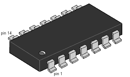
The surface-mount 4584B IC
Don't press too hard with the clip or the iron and don't move the
component with the iron as this will make it stick to the tip and
cause it to heat up too much.
When you have soldered one end, wait a few seconds before soldering
the other as this will allow the component to cool and prevent it
getting too hot.
This is important as the temperature of the tip of the iron will be
about the absolute maximum any of the components can tolerate and
the only way to prevent damage is to limit the soldering time to one
or two seconds.
The reason for this is the junctions of the semiconductors are very
close to where the soldering is taking place and any overheating will cause
degeneration in performance and even premature failure. The LEDs are
also very critical as the light-emitting crystal will lose its
output at the slightest amount of overheating. The transistor will
lose gain if overheated while the signal diodes are slightly more
tolerant however they become leaky if subjected to too much heat.
The electrolytics can also suffer considerably by overheating, so
take care.
While taking care with the temperature and soldering times, you must
also remember the orientation of the components as they will not
work if placed around the wrong way. The placement of the transistor
is fairly obvious as it has three leads and you can see which way
around it goes. The diodes come in the same package as the
transistor and you must not confuse the two.
The collector of the transistor is in the centre of one side and the
base and emitter terminals on the other side. Refer to the figure
below to
identify the terminals.
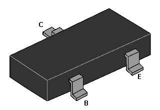
The pin-out of the surface mount BC 848 transistor
The cathode of the diode is in the centre of one side of the chip
and one lead on the other side is the anode. The third lead is "no
connection."
If the LED is a 2mm axial lead type, the cathode lead is marked with
a cross. Or if it is a genuine surface-mount LED, the pin in the middle
of one side is the cathode. This lead must be placed over the letter
"k" on the board.
The piezo is fitted to the two lands marked "Piezo" and the leads
can be soldered either way around as the piezo operates on AC and is
not polarised.
A single 3v lithium cell is fitted under two tinned copper wire
straps at one end of the board to supply power to the circuit. These
straps are made by placing the cell in position and bending the
copper wire over it and through the holes. They are then soldered
in position. The straps connect to the positive of the cell while
the negative makes direct contact with the board. The straps should
keep the cell tight so that it makes good contact with the board.
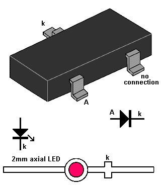
The pin-out for the diode and LED.
When the cell is fitted, the LED will begin to flash and the piezo
will produce a sound similar to a phone ringing.
If it doesn't, you may have a fault and if this is the case, you can
count yourself lucky as you will be able to go over the project and
diagnose the fault with the assistance of our "If It Doesn't Work
section." This is where you will start to learn about electronics
and the project will have great benefits.
IF IT DOESN'T WORK
If the circuit doesn't produce a sound similar to a phone ringing,
you will have to work out where the fault is coming from by reading
this section. There are possibly over 50
faults with a circuit as simple as this as any two components could
be swapped, any of them could be faulty due to overheating or the
board could have a short between the tracks.
To locate the problem, here is the approach:
The first thing to do is measure the internal impedance of the
battery. This is done by setting the multi-meter to 500mA range and
placing the probes on the battery for 1/2 second. The needle should
rise to about 200mA or more to indicate the cell can supply driving
current.
Next, measure the current taken by the circuit by placing a piece of
plastic under the cell so it doesn't make contact with the
board. This plastic can be used as a switch to turn the project off
when not required. Measure across the plastic with a multimeter set
to 50mA (or 500mA to be on the safe side). The current should be
about 1 to 2mA and you can change the range to 5mA to get an
accurate reading.
If it is considerably more than 2mA, you have either damaged one of
the components or created a short.
Make sure there are no solder bridges between tracks or under the
chip by inspecting the board carefully. Next cut the negative track
going to pin 7 of the chip so that half the circuit is removed.
Re-measure the current to see if the remaining parts contain the
fault. Refer to the circuit diagram to identify which components are
in this section and if the fault persists, make another cut in the
trackwork and "home-in" on the fault. This will save you removing
any of the parts and testing them, as soldering and desoldering will
create more problems than it solves.
If this doesn't find the fault, you will have to read on. In this
type of project we start at the back-end and work to the front. This
is because we have a LED and piezo to act as output devices to let
us know what is happening and the extent of the fault.
We start with the LED and its driver transistor. If the LED does not
light, the fault could lie in either of these components or the
chip.
To locate the problem, take a voltage reading at output pin 12 of
the chip.
The needle of the multimeter should flicker to correspond to the
ringing of the circuit and if not, the fault will lie in the chip or
one of the four oscillators.
If the needle flickers, go to the collector of the transistor. Here,
you will see the needle sit at slightly above 1v (due to the
characteristic voltage drop across the LED plus a very small drop
across the resistor) and fall to slightly less than 1v when the
circuit produces ring pulses. If the LED does not produce a glow
when this occurs, it has either been damaged or is around the wrong
way. If the needle does not flicker at the collector, the transistor
has been damaged.
You can also measure the voltage at the base of the transistor. The
reading you will get will only be about 100mV as the needle will not
have time to rise to 650mV during the ring. To get an accurate
indication of the signal you must measure it with a CRO.
If the sound from the piezo is not similar to that of a phone
ringing, the fault will lie in one or more of the 4 oscillators.
Start at the first oscillator, between pins 1 and 2. Place the
positive probe on pin
2 and set the multimeter to a low voltage. The needle will go high
for about 1 second and low for the same duration. When the output is
LOW, a tone is emitted from the piezo. If the output does not swing
up and down, measure the voltage across the power rails (pins 7 and
14) of the chip.
If voltage is present, and the current consumption is about 2mA, the
fault may lie in a damaged Schmitt inverter, a leaky 1u capacitor
or an open 2M2 or 1M resistor.
You cannot measure across the 1u while the circuit is operating as
the resistance of your meter will prevent it charging to 2/3 of rail
voltage and the oscillator will not change state.
The only thing you can do is measure the output voltage. If it is
HIGH, the input will be low (assuming the gate is working) and one
of the feedback resistors may be open circuit. Set your multimeter
to 10v range (assuming a 20k/v meter) and place the probes firstly
across the 2M2 resistor and then across the 1M. If you detect a very
slight movement of the needle, the circuit is working and the
resistance of the meter is taking the place of the resistor.
Replacing the appropriate resistor will fix the fault.
If the circuit produces a ring-ring-ring-ring without a pause, the
gating diode between pins 2 and 3 may be faulty or not making
contact.
If the output of the first oscillator is correct, the output of the
second can also be detected on a multimeter by probing pin 4. This
pin will give two High's during the ring tone and if a fault exists,
you can diagnose it in a similar manner to the first gate.
The output of the third and fourth oscillators are more difficult to
detect on a multimeter as the frequency is too high for the needle
to respond.
The solution is to remove the piezo from its output terminals and
place it between pin 6 and the negative rail. Here you will hear a
series of clicks to correspond to the 33Hz oscillator, gated by
oscillator (b).
Placing the piezo between pin 12 and the negative rail will produce
the ring sound except the output will be lower than when connected
to the output terminals.
If you find one of the inverters has been damaged, you can use the
one between pins 8 and 9. You will have to do a little rewiring,
however if the chip is not drawing excessive current due to it being
damaged, the change can be made. This just about covers everything
and the project should be working perfectly by now - I hope so.
CONCLUSION
If you did not have any success, the best solution is to buy another
kit and start again. The main problem will be soldering. Next time you will
learn from your mistakes and the project will work first go. For those who
have tasted the joys of success, try some of our other projects using
surface-mount technology.