|
Prototyping Boards |
Prototyping boards are available from
Talking
Electronics.
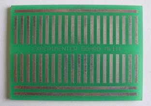
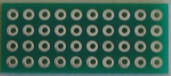
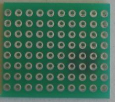
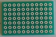
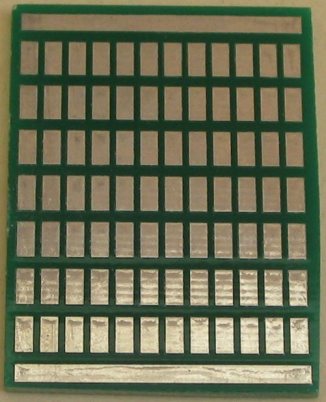
P2 Matrix Boards
![]()
|
SPECIAL OFFER You get 12 mixed boards for $10.00 Plus $4.00 postage The boards are: 1 off: 20 x 15 holes 1 off: 38 x 11 holes 1 off: Surface Mount Board MkIII and 1 - 15x40 SM-2 2 off: 7 x 5 holes, 10 x 4 holes, 10 x 8 holes, 12 x 11 holes  (This link will send an email to Colin Mitchell and you will be
advised how to send money via Paypal)
(This link will send an email to Colin Mitchell and you will be
advised how to send money via Paypal)You can also get individual prices for boards. |
| Or email Colin Mitchell with the type of boards you require. |
It doesn't matter if you are designing a new
microcontroller project or a simple transistor amplifier, the first
necessity of designing a project is the ease of
changing components.
If you think a project will work without testing, modifying and
altering things, you are kidding yourself.
It sometimes takes hundreds of changes to get a project working
perfectly.
And if the components are not easy to change, you may be reluctant to do
the finer adjusting.
That's why a prototyping board must be designed for easy access and must
be universal, so that all types of components can be fitted.
Strip-board is a failure. You have to cut the copper track with a sharp knife and this is very messy. Here is an example:
If you just want to build a circuit, see it work, then pull it apart,
you can use a BREADBOARD.
This is one of the worst breadboards. It does not have any positive and
negative rails:
This is the best breadboard with TWO power rails. When the board is placed as shown, the positive and negative rails are close to the components. The only problem with this type of board is fitting components with thick leads such as power transistors, regulators, switches etc.
If you are designing 10 projects at the same time, you will quickly run
out of breadboards.
They are also quite unsuitable for RF projects.
Breadboards also have a problem of wires touching and connections
becoming noisy.
Also, the connections become loose after a thick lead has been inserted
and thin pins do not touch the contacts. This especially applies to IC
sockets where one or more of the pins will not make contact and you will
spend hours trying to find the fault.
The solution is a PROTOTYPING BOARD
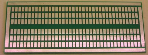
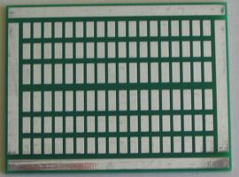
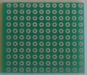
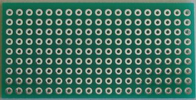
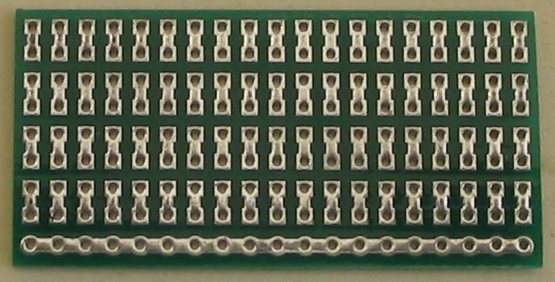
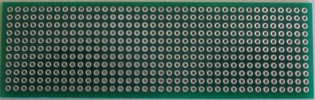
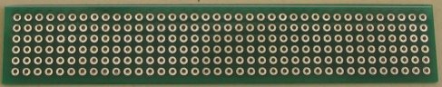
Here are some prototyping boards from Talking Electronics:
Surface Mount Board MkIII
Surface Mount Board 15x40 SM-2
40mm x 105mm
$2.50 each
14 x 20 Surface Mount $2.50
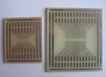
Two surface-mount boards from
the range from Talking Electronics
$2.50 each 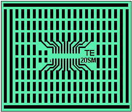
This board accepts a 20 pin Surface Mount chip
$2.50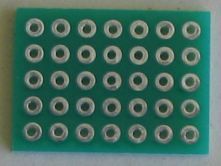
7 x 5 holes
10 x 8 holes 50cents
11 x 7 holes
50cents
12 x 11 holes
$1.00
9 x 19 holes
$1.50
also:
15 x 12
$1.50
20 x 15 holes
$2.50
16 x 12 Surface Mount
$2.50
9 x 20 Surface Mount
$2.50
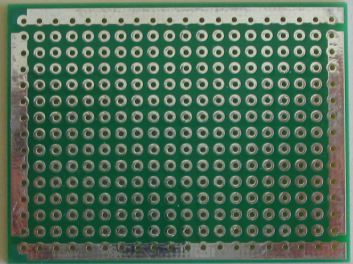
11 x 38 holes
(double-sided - PTH)
$2.50
Some prototyping boards are not designed to look beautiful. They are designed
to be functional and reduce frustration.
Many prototyping boards on the market are quite useless. They are not
really prototyping boards but rather "Universal Boards" that will accept
different components and hand wiring.
If you are thinking of going to the next
step and designing a PC board for your project, here are a few tips:
http://techdocs.altium.com/display/ALEG/Legacy+Downloads
You can contact me (Colin Mitchell) for a list of features on how to drive the software.
http://www.tsien.info/ (boardmaker)
Some software will freeze-up and you will lose everything you have done.
Other software cannot be saved as a file. Some software cannot be sent to any PCB
manufacturer . . . it can only be sent to the expensive manufacturer that
supplies the software.
Gerberview websites:
Here is an interesting discussion on CAD
programs:
50 Top Product Design and Product Development Software Tools
MORE
Here's a list of 14 FREE CAD packages from:
http://www.edn.com/electronics-blogs/all-aboard-/4441802/3/Free-PCB-ECAD--The-Ultimate-list
The website shows some amazing things you can create with these
packages.
PCB DESIGN SOFTWARE
https://www.electroschematics.com/2249/pcb-design-software/ 0
PCBWeb Designer
HOW A PCB IS MADE
These are the steps to make a PCB:
P2
Matrix Boards
6 x 38 holes
$1.50
also
6 x 40 holes
$1.50
5 x 18 holes
$1.00
5 x 23 holes
$1.00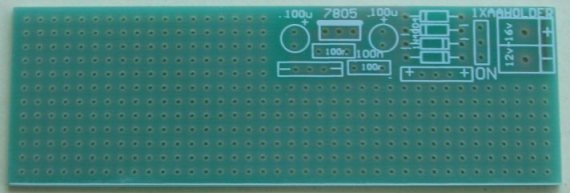
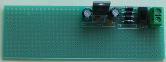
10cm x 3cm Matrix Board with POWER SUPPLY
- built-up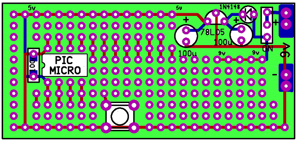
This board is specially
designed for a PIC chip with the power rails
to the chip already provided.
It is designed to allow you to produce a very fast, neat prototype.
There is a 5v rail from the regulator and a 9v rail from the battery.
The battery clips directly to the board or via a battery-snap.
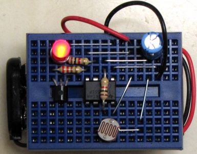
A prototype project is sometimes called a "rats-nest" or "birds-nest."
There are two levels of prototyping.
The first level requires no experimenting. It's simply building a
"proven" circuit on a board and connecting it to other items.
The second level involves experimenting and changing component values.
For this, the components should be on one side of the board.
The end-result is a jumble but it's the only way to be able to get-to-everything
and see the whole circuit:
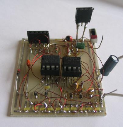
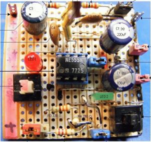
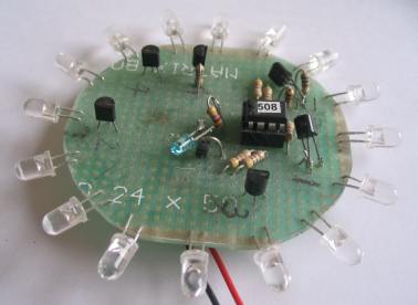
11 LEDs and surface-mount components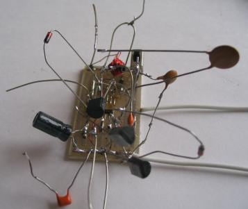
design and before the final board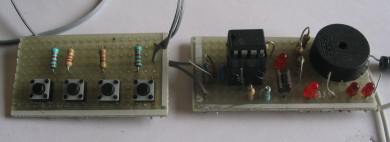
Using a Matrix Board for designing
The essential part of a prototyping board is the accessibility of each
and every component so the voltage and waveforms can be measured.
But the most important reason is each component must be easily removed
and/or replaced. That's why soldering components through holes is not
suitable. Sometimes a component has to be changed 4 or 5 times. Imagine
the difficulty in pulling out a component every time you want to alter
the value.
Some of our prototype boards have certainly become over-crowded but
that's how a circuit gets designed.
Initially you think the circuit will need a few components and choose a
small PC board. It quickly gets over-crowded but as the circuit
develops, you can easily see what each component is doing and it's
really not complex at all.
You will notice many of the circuits in the photos above have been
designed with surface-mount components.
These are just as cheap as normal components and since they take up less
space on the board, it creates less clutter and you can see what you are
doing.
Surface-mount
kits are available from Talking Electronics and when combined with
the prototyping boards, you will be able to develop circuits that are
very compact.
The second step before making a PC board is to lay out the components on
a matrix board in the same locations as they will appear in the final
design.
This will give you two answers. It will let you know if the project will
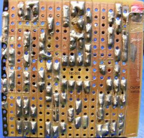
work and give you some idea of the size of the board and where each item
is positioned. The underside of the board is generally a mass of fine
wiring and it may need one more layout to produce wiring that does not
cross at any location. Any wires that cross each other need a jumper and
by carefully re-laying the board, no jumpers will be needed. Here is our
example of the PIC Lab-1 before the final PC layout. The stage before
this was a "rats-nest" and the final design you can see in the PIC Lab-1
article.
If you think our projects "magically appear from no-where" you should
see our boxes of thousands of prototypes!
The second step to making a PC
board
DO NOT use PCB software associated with any PC manufacturer. You are
LOCKED-IN to their costing and it is generally EXORBITANT.
Do not accept "touts" sending you emails from PCB manufacturers. These
costings are also very high and generally the person behind the email is
working from home as a "go-between." They MARK-UP the prices from the
manufacturer and you don't get a bargain.
Here is a website that compares the cost of making a PCB from different
manufacturers:
http://pcbshopper.com/
Many of the manufacturers are a RIP-OFF They quote $36.00
for 3 boards plus $15.00 delivery.
But the size of the board is 3cm x 3cm.
Who wants a board 3cm x 3cm ????
When you peel away all the SCAMs, there are only a few manufacturers who
offer low prices.
The cheapest and best is:
http://www.elecrow.com/
They produce 10 panels 10cm x 10cm double-sided green solder
mask, PTH, HASL with white legend on top and bottom for $12.00
Plus $9.00 shipping.
The quality is perfect and you could not buy the materials for $12.00
The only problem with low-cost boards is the size. You have to keep the
size smaller than 10cm x 10cm.
Any board over 10cm x 10cm costs 300% more and you will find this
provides a very good learning-curve to producing modular systems with a
maximum footprint of 10cm x 10cm.
You can stack the board on top of each other or provide plugs and
sockets to join the edges.
This way you can produce an OUTPUT BOARD, POWER SUPPLY BOARD, display
board and a number of INTERFACE BOARDS and create a whole range of
different produces with a small number of modules.
If you really want the simplest software for designing a simple board, try this
FREE software:
Autotrax
DOS Freeware version 1.61 - Complete PCB layout package with output
support for printers, pen plotters and Gerber.
To install: Download and run the file in the root
directory of your hard drive to extract the install program. The install
program must be run from the root directory.
Download (ZIP 821 KB)
EasyTrax
DOS Freeware version 2.06 - Complete PCB layout package with output
support for printers, pen plotters and Gerber.
System requirements: PC-compatible; DOS 2.0 or later; 640K RAM; 2Mb of
hard disk space.
I have been using the same DOS software for 40 years because no software
is compatible with other programs and when you want to make a panel of
15 different boards, they must all be developed from the same software.
Many free software packages only allow you to make a small board or a
limited number of holes or you cannot export the file or some other
frustration.
That's why I keep using the simplest package:
Autotrax.
Here are some replies from readers who have used different
packages and found the pit-falls:
SoloPCB can be seen at
http://www.fabstream.com/solopcb-design-software.php
Designspark PCB: Requires a registration which is free but it’s
bug-ridden and last time it didn’t work. Support couldn’t solve it.
Later I realised it required constant connection to the net with cookies
enabled.
It's to hard to use. And
the schematics it produces look terrible. The only thing I can see that
it's good for, is if you need to make a really big PCB. Because you can
make a up to a 14 layer board, and it has no pad number restriction.
Also, it has a 3D PCB function.
Diptrace
It's the best EDA software I have ever used! It has a HUGE library of
parts, and a really neat 3D PCB feature. And it's super easy to use!
It's documented better then any EDA program I have ever seen.
Fritzing is a toy.
Kicad I found to be full of bugs to the extent of uselessness. I
deleted it when I found myself fighting the software rather than
designing a PCB.
It's really easy to figure
out, but it takes to long to do anything in it.
FreePCB wasn’t maintained for the last three years – since 2011. This
tells the story.
All I remember about it is,
I did not like it, and uninstalled it within two days of getting it
(that's most likely not very helpful).
OsmondCocoa (http://www.osmondpcb.com/index.html)
Unfortunately, you can only do PCBs in it. It's really good if you have
a Mac computer, and it's also really easy to use.
TinyCad is what the name says: tiny. The library is extremely limited.
For example there are only 11 microcontrollers.
ExpressPCB is anything but express. Very difficult to use it. If you
re-position a part, you have to re-align every-single-connection going
to it. This means, every corner of every line. This is perhaps the most cumbersome to use among all of these. Badly limited library.
ExpressPCB/ExpressSCH
(http://expresspcb.com/ExpressPCBHtm/Free_cad_software.htm)
Really great program, easy to use, and it produces really nice
schematics. Only thing I don't like about it is, you can't export boards
to send to manufacturers other then ExpressPCB.
ZenitPCB (http://www.zenitpcb.com/)
I could never figure out how to use it. It looks like it would be very
useful if it had better documentation.
LIST OF EDA SOFTWARE (ELECTRONICS DESIGN AUTOMATION)
These packages include schematic "capture" and PCB layout. Some include
autorouters. The commercial packages also include autorouters,
simulation, and other features.
Web-based (run in browser):
Free and low-cost packages:
123D Circuits
http://www.123dapp.com/circuits
-
Upverter
http://www.upverter.com
Free for publically visible designs
EasyEDA
http://easyeda.com
-
Professional with free limited versions:
AutoTRAX DEX 2020
http://www.dex2020.com/
Free trial; full price USD 49; not related to Protel Autotrax
DesignSpark PCB
http://www.rs-online.com/designspark/electronics/page/
designspark-pcb-home-page
Free (non-commercial and commercial); affiliated with RS Components.
Anon: Requires (free) registration; buggy; requires constant
internet connection with cookies enabled. Supercap2F: Too hard to
use; schematics look terrible; supports large sizes and many layers;
has 3D PCB view.
Eagle
http://www.cadsoftusa.com/
Windows/Linux/Mac. Widely used. Free version has limitations. Can
only do 90mm x 90mm board!!
Quite useless as most PCB makers will make 100mm x 100mm for $10.00
ExpressSCH, ExpressPCB
http://expresspcb.com
Windows only. Anon: Very difficult and cumbersome to use; moving a
component requires manual realignment of all connections to it; very
limited library. Supercap2F: Great program, easy to use, produces
really nice schematics, but cannot export boards to send to
manufacturers other than ExpressPCB.
FreePCB
http://www.freepcb.com/
Anon: Not maintained since 2011. Supercap2F: I did not like it
Fritzing
http://fritzing.org/
Schematics, PCBs, breadboard and stripboard layouts. Anon: "a toy".
gEDA suite
http://www.geda-project.org/
Posix/Linux; GPL
KiCAD
http://www.kicad-pcb.org/
This has been referenced by Elektor to be the best free CAD program
to make your own boards. Version 4.0.7
PCB123
http://www.sunstone.com/pcb-products/pcb123
Windows only. They offer PCB manufacturing services
Protel Autotrax and EasyTrax
http://techdocs.altium.com/display/ALEG/
Freeware downloads
MS-DOS - use DOSBox (http://www.dosbox.com)
under Windows
TinyCAD
http://sourceforge.net/projects/tinycad/
For schematics (includes netlist export) and line diagrams. Anon:
Library is extremely limited - there are only 11 microcontrollers.
Good reviews on sourceforge.
ZenitPCB
http://www.zenitpcb.com/
Supercap2F: Could be good if it had better documentation.
Professional without free or cheap versions:
Bartels AutoEngineer
http://www.bartels.de/bae/bae_en.htm
Windows, Linux, X11/Unix. Schematic is free; PCB has a free demo
version
But you may not be able to use the free version to make a PCB.
Bartels AutoEngineer Light,
the entry level system for double-sided PCBs up to euro format size
(160 × 100 mm) is
159 Euro plus
VAT and delivery.
Cadstar
http://www.zuken.com/en
Free version limited to 300 pads and 50 components
DipTrace
http://www.diptrace.com/
Windows/Linux. Free version limited to 300 pads and 2 layers.
KrisBlueNZ: Produces very nice-looking schematics. Supercap2F:
Highly recommended. Huge parts library; 3D PCB view; very easy to
use; very well documented.
OsmondCocoa
http://www.osmondpcb.com/index.html
Mac only. Free version limited to 700 pins. Supercap2F: PCB only.
Very easy to use.
Target 3001
http://ibfriedrich.com/
Free version limited to 250 pads and 2 layers
VUTRAX
http://www.vutrax.co.uk/index.htm
-
Altium
-
Formerly Protel
Boardmaker
http://www.tsien.info/
3D viewer. KrisBlueNZ: Looks expensive!
CIRCAD
http://www.holophase.com/index.html
-
EasyPC
http://www.numberone.com/
Free version can’t save nor generate output
EDWinXP
http://www.visionics.a.se/
Evaluation period is 14 days
Multisim
http://www.ni.com/multisim/
Schematic capture and SPICE simulation; see Ultiboard
OrCAD
http://www.orcad.com/
-
PADS
-
-
Proteus
www.labcenter.com/
-
Pulsonix
http://www.pulsonix.com/
-
Sprint-Layout
http://www.abacom-online.de/uk/html/sprint-layout.html
Inexpensive
Ultiboard
http://www.ni.com/ultiboard/
PCB option for Multisim
http://www.ni.com/ultiboard/
http://www.abacom-online.de/uk/html/sprint-layout.html
http://www.cadcam-group.eu/electronics/software/p-cad/ (PCAD)
http://www.rimu.pl/hs/rimuuk.html (RIMU)
Here is an interesting article from David L. Jones on the terminology
you need to know when designing your own Printed Circuit Board:
PCB Design Tutorial
http://sourceforge.net/projects/gerbv/
http://www.easylogix.de/products_detail.php?prog_id=1
http://www.pentalogix.com/viewmate.php#main-content
Does anyone know of a Good Free EDA design package?
I have been looking for a good free EDA design
package, I have looked at Design Spark ,Ki cad, and Easy EDA. Has anyone
recommend a EDA package that has stable parts and components and that is
easy to use.
I’m not sure any decent EDA suite will have “stable parts and
components”. That may suggest it is stagnant!
Answer from ANDY FIERMAN:
Of all the free EDA tools, I can recommend EasyEDA.
It is still in the earlier stages but is developing rapidly into a very
capable EDA tool for schematic capture and PCB layout (up to about 6
layers).
It includes simulation too.
It has a lot of library parts but the single thing that makes it stand
out is that it is easy to learn to drive.
That means that even if the part you need is not there already, it’s
easy to create your own and that automatically gets shared with the
whole library so the library builds up very quickly.
EasyEDA has several import options for Eagle, KiCad and LTspice files.
It also has several export options (have a look at their Tutorial).
KiCad and gEDA are more powerful cross-platform tools but are quite hard
to learn. Being FOSS, they have open file formats. Simulation is not
well integrated with them.
Design Spark is developing well but I don’t know much about using it. I
assume it has open file formats. It’s import and export look reasonably
good.
expressPCB is another free tool but watch out for being tied into buying
PCBs from them.
Even though EasyEDA offers a low cost PCB service, they don’t tie you
into using it. Gerbers can be downloaded and sent to any PCB fab.
The thing I don’t like about being tied to a PCB vendor is that you do
all the work and then you end up with nothing you can carry away with
you.
And if you seriously want to do controlled impedance work then
you must have the freedom to choose your PCB materials, stackup and
maybe even fab house.
EasyEDA supports a single set of PCB track design rules but tracks can
be modified on a per track basis so you can manual define tracks that
you need to be specific widths.
For a defined impedance you will then have to specify a substrate
material and – if it’s really important – a material manufacturer.
You will also have to specify the layer spacings. EasyEDA currently uses
a default set of layer spacings and the material is uncontrolled. You
can contact EasyEDA via their support email address to discuss your
requirements or to find out what the default stackup and materials are
and then design the trace widths to suit.
If that isn’t enough then you still have the option to specify what you
want in the design in EasyEDA, generate and download the Gerbers at the
end of the design and then take them to a PCB fab house than can make
exactly what you want.
That’s the crucial bit that you can’t get with a tied-in free tool.
I don’t think any online tool (certainly not a free one, unless the free
version of Upverter supports it?) allows you to define a trace impedance
and then have it work out the required trace width for you on a given
substrate and stackup.
KiCad has a trace impedance calculator built into it but that is not
tied into any form of Design Rule definition or checking. There are many
similar online trace impedance calculators that would give adequate
trace dimensional information consistent with the degree of impedance
control precision you might be able to achieve using EasyEDA.
It’s not until you get up to the higher end tools like Altium (maybe),
Cadence and Mentor that you get true controlled impedance design
capability. In tools like that you can specify the detailed layer
stackup and then specify trace impedances in the schematic. Then they
are passed through into PCB layout and actually define the trace
dimensions.
All of that information is then used to run Signal Integrity simulations
and, in some tools, RF and Microwave simulations.
That said, it is possible to create quite effective simulations of
controlled impedance circuits in EasyEDA because the underlying spice
engine supports a range of transmission line structures.
It’s fiddly to set up and again is not tied into the PCB design rules in
any way: it just shows what the circuit would do if the PCB had all the
right impedances in it. You still have to manually calculate all the PCB
trace width and stack-up dimensions, taking into account the dielectric
constant of the substrate material. That can be partially automated by
building parameterised expressions into the simulation to incorporate
those given substrate parameters. If you wanted to go into that much
depth, I’m sure contacting support at EasyEDA would get you some further
guidance on this.
http://www.pannam.com/blog/best-product-design-software-tools/
The link above covers 50 CAD packages that allow you to produce a
PCB from a circuit or from laying out the board yourself.
Remember, some of the FREE packages from PCB manufacturers only allow
the board to be made by the company that has supplied the free software
and they generally charge a lot more than the Chinese manufacturers.
In addition, you cannot get the artwork without paying a lot for it.
The free package ends up a lot more than using a package that is not
tied to any manufacturer.
If you are just starting out, you need to use the simplest software
because that is all you need and keep to the same package as you will
need to import older boards when you make new panels.
The cheapest is to get 1, 2, 3, 4 or 5 boards on a panel 100mm x 100mm
and cut them yourself with a hacksaw. Make sure the cut lines can be
done with a saw. You can get 10 panels for $25.00 incl post from:
http://www.elecrow.com/
without any complex forms on the web and without any tricks.
It's wonderful to have a CAD package that creates a CIRCUIT BOARD
from a schematic.
But there are a number of things you have to remember.
These types of packages has a lot of automatic or "controlled" features
that make it difficult for you to "do your own thing."
It's only a completely manual package that gives you full control.
On top of this, some packages are very difficult and time-consuming to
learn and things such as "reverse reading" of text may takes you hours
to work-out.
The first thing to do is try a number of packages and make sure thy can
be saved to a file and then sent to a manufacturer. Some packages can
only be sent to one manufacturer and the cost will be very high.
When you are satisfied with a package, it will be the only one you use
for ALL
your boards.
It may not be possible to combine two programs and thus you
will not be able to import old boards to your recent panels. So, stick
to a single package.
Stick to dimensions up to 10cm x 10cm as this is the cheapest panel to
get processed and if you are thinking of making boards larger than this, consider
creating modules of 10cm x 10cm and plugging them together.
This will make manufacturing and servicing easier and cheaper.
When creating the layout, you need to place the major components on the
layout in places where you want them. The program will then connect them
via tracks. Always use a double-sided board as this is the cheapest
option.
Always identify EVERY component on the board so you can build it without
referring to any other list of materials.
Give every board a name, add your email address and date of manufacture,
so anybody can contact you if a fault occurs.
When you have hundreds of boards, you will appreciate this. Customers
email after 10 years and want a replacement.
Now we come to the technical side.
Don't expect a project to work perfectly the first time.
You may need to add or move a component or add more text.
If these changes are major, re-name the board with a new serial number and make sure the old
boards are placed in a sealed bag and destroyed when the new boards
arrive.
When making changes, you will appreciate software that allows you to
move any track or component without moving other tracks on the
board.
Some software moves tracks "off the screen" and when you zoom out, the
whole board is messed up.
You also need to be able to change the size of any track or pad to make
modifications, so make sure the software can do this before deciding on
the package you will use.
Always save your work after 10 changes so you can go back to a
previous board if you make a mistake.
Use the simplest software package so you are in charge and able to make your own
modifications without being limited to angles, widths, sizes etc.
If you get frustrated with a package, try another. There are over 30
packages on the web.
Once you enjoy making boards you will want to create something every few
days.
I have been making boards for over 30 years and I am creating a new
board every week.
I use the first CAD package to be invented PROTEL (Easy Trax
version). It has NEVER fallen over, crashed or frozen-up. Unlike some of
the other packages that run out of memory when you are trying to combine
boards.
It is up to you to choose a package and stick with it and enjoy the
reward of making your own boards.
It is not economical making one board at a time.
You can fit 5 small boards on a 10cm x 10cm panel and only get the outer
edge routed. This will cost $25.00 posted for 12 panels.
Make sure you can cut the boards yourself with a hack saw and allow 70
thou between boards for cutting.
Linish the edges with sandpaper and you will have expertly made boards.
And finally, the most important tip of all.
As you get a collection of boards, you can use various parts of the
previous boards to help create a new board.
This is a very good idea because you know the size and shape of the
components is correct and things like switches and sockets will fit the
board without any problems.
You also need a digital caliper to measure different components to make
sure the spacing is correct.
All boards are measured and created in inches but the final boards have to fit in
a 10cm x 10cm (3.93inches) panel. I know it is messy but digital calipers cost
less than $25.00 and are useful in the workshop for measuring all sorts
of things. They are especially useful when making components (for your
own library) such as switches, to get the spacing correct.
Here is a set of notes and more references to additional PCB design
packages:
http://www.electro-tech-online.com/threads/the-scoop-on-pcb-layout-software.111236/
(copy and past if this link does not work inside this frame)
There are some manufacturers that combine your boards with those of
others and charge by the square inch.
You have to do your own research before starting - to find out
which is the cheapest and best for your situation.
In the end you will get great satisfaction in creating a compact board
from a very complex design.
These designs take years of experience to master.
Just start with simple boards and get the satisfaction of seeing your
ideas come to life.
Work up gradually and make sure you use a package that does not make you
frustrated.
Making PC boards is one of the best things you can do. It is so
rewarding.
Do you need a free PCB design software or
tool to put in practice the new electronic project
you’ve just designed? So, we present you 10 of the best
PCB software tools available on the internet that will
help you to develop your printed circuit board faster
and with ease.
PCBWeb is a free CAD application for designing and
manufacturing electronics hardware. Design multi-sheet
schematics with our fast and easy-to-use wiring tool.
Route multi-layer boards with support for copper pours
and DRC checking. Integrated Digi-Key Parts Catalog with
Bill of Materials Manager.
1
ZenitPCB
Is an excellent pcb layout design software tool to
create professional printed circuit board ( PCB ). It is
a flexible easy to use CAD program, which allow you to
realize your projects in a short time. With ZenitPCB
Layout is possible to create the project starting both
from the schematic capture or by the layout itself.
2
TinyCAD
Is a program to help you draw circuit diagrams. It comes
complete with symbol libraries to get you started
straight away. As well as being able to simply print
your designs, you can use TinyCAD to publish your
drawings by copying and pasting into a Word document or
saving as a PNG bitmap for the web.
3
Osmond PCB
Is a flexible tool for designing printed circuit boards.
It runs on Macintosh. Its many features include:
virtually unlimited board sizes, number of board layers,
number of parts, support for both through-hole and
surface mount parts and more.
4
BSch3V
Is a schematic capture program for Windows. The name
“BSch” is an abbreviation of “Basic Schematic”. It has
only basic functions, in order to simplify operation.
6
Kicad
Is an open source (GPL) software for the creation of
electronic schematic diagrams and printed circuit board
artwork. It is useful for everybody working in
electronic design (schematic diagrams and Printed Board
up to 16 layers).
7
gEDA
Runs on Linux and has produced tools which are used for
electrical circuit design, schematic capture,
simulation, prototyping, and production. Currently, the
gEDA project offers a mature suite of free software
applications for electronics design, including schematic
capture, attribute management, bill of materials (BOM)
generation, netlisting into over 20 netlist formats,
analog and digital simulation, and printed circuit board
(PCB) design layout.
8
Fritzing
Fritzing software is an interesting open-source
initiative to support designers, artists, researchers
and hobbyists to work creatively with interactive
electronics and develop electronic projects. Fritzing
helps you learn more about electronic circuits, to
document your projects and even let’s you prepare them
for production.
9
DesignSpark PCB
DesignSpark PCB is the world’s most accessible
electronics design software. Easy to easy to learn and
easy to use, it is designed to significantly reduce your
concept-to-production time. At the core of this unique
approach is a powerful software engine that enables you
to capture Schematics, design PCB boards and layouts.
10
EasyEDA
EasyEDA is a free, zero-install, Web and cloud-based EDA
tool suite, integrating powerful schematic capture,
mixed-mode circuit simulation and PCB layout in a
seamless cross-platform browser environment, for
electronic engineers, educators, students and hobbyists.
1 PPE - Pre Production Engineering
Customer supplied data (gerber) is used to produce the
manufacturing data for the specific PCB (artworks for
imaging processes and drill data for drilling programs).
Engineers compare demands/specifications against
capabilities to ensure compliance and also determine the
process steps and associated checks.
2 Preparing the phototools
Artwork Master is PCB production in the key steps, which
directly affect the quality of the final product
quality. An accurately scaled configuration of electronic
data used to produce the artwork master or production
master. Artwork Master – The photographic image of the
PCB pattern on film used to produce the circuit board,
usually on a 1:1 scale. In general, there are three types
of Artwork Master: (1) Conductive Pattern (2) solder
mask (3) Silkscreen.
3 Print inner layers
Stage 1 is to transfer the image using an artwork film
to the board surface, using photosensitive dry-film and
UV light, which will polymerise the dry film exposed by
the artwork. This step of the process is performed in a
clean room. Imaging – The process of transferring
electronic data to the photo-plotter, which in turn uses
light to transfer a negative image circuitry pattern
onto the panel or film.
4 Etch inner layers
Stage 2 is to remove the unwanted copper from the panel
using etching. Once this copper has been removed, the
remaining dry film is then removed leaving behind the
copper circuitry that matches the design. Etching – The
chemical, or chemical and electrolytic, removal of
unwanted portions of conductive or resistive material.
5 Inner layer Automatic Optical Inspection (AOI)
Inspection of the circuitry against digital “images” to
verify that the circuitry matches the design and that it
is free from defects. Achieved through scanning of the
board and then trained inspectors will verify any
anomalies that the scanning process has highlighted.
6 Lay-up and bond (Lamination)
The inner layers have an oxide layer applied and then
“stacked” together with pre-preg providing insulation
between layers and copper foil is added to the top and
bottom of the stack. The lamination process consists of
placing the internal layers under extreme temperature
(375 degrees Fahrenheit) and pressure (275 to 400 psi)
while laminating with a photosensitive dry resist. The
PCB is allowed to cure at a high temperature, the
pressure is slowly released and then the material is
slowly cooled.
7 Drilling the PCB
We now have to drill the holes that will subsequently
create electrical connections within the multilayer PCB.
This is a mechanical drilling process that must be
optimised so that we can achieve registration to all of
the the inner layer connections. The panels can be
stacked at this process. The drilling can also be done
by a laser drill.
8 Electroless copper deposition
The first step in the plating process is the chemical
deposition of a very thin layer of copper on the hole
walls. PTH provides a very thin deposit of copper that
covers the hole wall and the complete panel. A complex
chemical process that must be strictly controlled to
allow a reliable deposit of copper to be plated even
onto the non-metallic hole wall. Whilst not a sufficient
amount of copper on its own, we now have electrical
continuity between layers and through the holes. Panel
plating follows on from PTH to provide a thicker deposit
of copper on top of the PTH deposit – typically 5 to 8
um. The combination is used to optimise the amount of
copper that is to be plated and etched in order to
achieve the track and gap demands.
9 Image the outer layers
Similar to the inner layer process (image transfer using
photosensitive dry film, exposure to UV light and
etching), but with one main difference – we will remove
the dry film where we want to keep the copper/define
circuitry – so we can plate additional copper later in
the process. This step of the process is performed in a
clean room.
10 Plating
Second electrolytic plating stage, where the additional
plating is deposited in areas without dry film
(circuitry). Once the copper has been plated, tin is
applied to protect the plated copper.
11 Etch outer layer
This is normally a three step process. The first step is
to remove the blue dry film. The second step is to etch
away the exposed/unwanted copper whilst the tin deposit
acts an etch resist protecting the copper we need. The
third and final step is to chemically remove the tin
deposit leaving the circuitry.
12 Outer layer AOI
Just like with inner layer AOI the imaged and etched
panel is scanned to make sure that the circuitry meets
design and that it is free from defects.
13 Soldermask
Soldermask ink is applied over the whole PCB surface.
Using artworks and UV light we expose certain areas to
the UV and those areas not exposed are removed during
the chemical development process – typically the areas
which are to be used as solderable surfaces. The
remaining soldermask is then fully cured making it a
resilient finish. This step of the process is performed
in a clean room.
14 Surface finish
Various finishes are then applied to the exposed copper
areas. This is to enable protection of the surface and
good solderability. The various finishes can include
Electroless Nickel Immersion Gold, HASL, Immersion
Silver etc. Thicknesses and solderability tests are
always carried out.
15 Profile
This is the process of cutting the manufacturing panels
into specific sizes and shapes based upon the customer
design as defined within the gerber data. There are 3
main options available when providing the array or
selling panel – scoring, routing or punching. All
dimensions are measured against the customer supplied
drawing to ensure the panel is dimensionally correct.
16 Electrical test
Used for checking the integrity of the tracks and the
through hole interconnections – checking to ensure there
are no open circuits or no short circuits on the
finished board. There are two test methods, flying probe
for smaller volumes and fixture based for volumes. We
electrically test every multilayer PCB against the
original board data. Using a flying probe tester we
check each net to ensure that it is complete (no open
circuits) and does not short to any other net. Good
products come from good manufacturing but not
inspection.
17 Final inspection
In the last step of the process a team of sharp-eyed
inspectors give each PCB a final careful check-over. Visual
checking the PCB against acceptance criteria. Using manual visual
inspection and AVI – compares PCB to gerber and has a
faster checking speed that human eyes, but still
requires human verification. All orders are also
subjected to a full inspection including dimensional,
solderability, etc.
18 Packaging
Boards are wrapped using materials that comply with packaging demands (ESD etcetera) and then
boxed prior to be being shipped using the requested mode
of transport.
Email:
jonny@apollopcb.com
Web:
www.apollopcb.com
15/4/2019
