| THE HEX SCHMITT TRIGGER |
| The 74c14 |
See Page 49 for the first section of this discussion.
We have already mentioned the 74C14 is one of the most versatile chips on the market.
It is also known by a number of identities: 74c14, 74HC14, 40014 and 40106. These are CMOS chips and are characterised by low current consumption, high inputimpedance and a supply voltage from 5v to 15v. (Do not substitute 7414 or 74LS14. They are TTL chips and operate on 4.5v to 5.5v and have low impedanceinputs.)
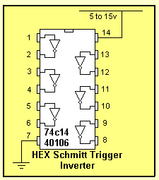
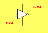
The Hex Schmitt Trigger IC contains 6 separate gates:
 |
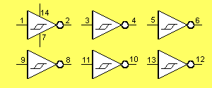
Each inverter can be used as a separate "block" or "building block" or "circuit" in a project. You can use 1, 2 or all 6 "gates." We can call the inverter a "gate." This is a very loose term as a "gate" normally has more than one input and the second input is used to activate or de-activate the gate.
The following diagram shows the six inverters:
Pin 7 is connected to the 0v rail, commonly called "negative" or "earth rail."
Pin 14 is connected to the positive rail (5v - 15v) - commonly called the "supply."
When the chip is connected to the "supply," all 6 inverters are connected to the power rails via circuitry inside the chip. This saves connecting each inverter to the supply!
If nothing is connected to any of the inputs or outputs, the chip will consume only a few micro-amps.
The action of a Schmitt Trigger is shown in the following animation.
The action shows the output changing rapidly as the input rises and falls. The output always changes from one state to the other VERY QUICKLY. The input can rise and fall slowly - the output is always a fast action. 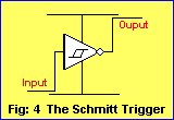
The actual voltage at which the output changes is not important in this discussion as we will be providing a voltage above 66% and below 33% to make sure the output changes from one state to the other.
There is one hidden feature of a Schmitt Trigger.
It is used in the circuits below because the gap between detecting a High and LOW on the input is about 33% of rail voltage.
This gap is called the HYSTERESIS GAP.
With many other inverter chips the gap between detecting a HIGH and LOW is very small.
If we use one of these inverters and take the input from 0v to rail voltage very slowly, the output will start to flutter when the input is about mid-rail, as shown in the animation below:
The inverter "jumps" when input at mid-rail
This is because the chip does not know if the voltage is a HIGH or a LOW.
The output can produce 10 to 100 "false pulses" during this time.
It requires the signal to go from one state to the other VERY QUICKLY and it is not suitable for slow rising and falling signals.
The SCHMITT Inverter is ideal for projects where "HUMAN INPUT" is involved - such as a push button, turning on equipment, photo-cell detection, magnetic inputs and anything where a slow-rising signal is present.
The
Thus the Schmitt Trigger Inverter becomes a very useful gate.
Here are some basic building blocks:
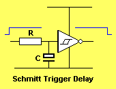
In the diagram above, the input goes HIGH and remains HIGH. It can be detecting a piece of equipment being turned on, for example.
The output goes LOW after a period of time called the "DELAY TIME."
The Delay Time is determined by the values of R and C. We are not concerned with the actual values of R and C at this point in time. They can be worked out by experimentation.
The point to not is the placement of the two components to produce a DELAY.
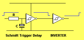
If the output is required to be the opposite of the circuit above, an inverter is added:
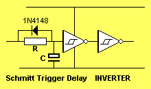
If a diode is added across the input resistor, the capacitor "C" will be discharged when the input goes low, so the "Delay Time" will be instantly available when the input goes HIGH:
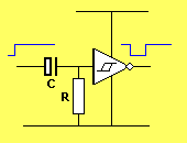
The following circuit produces a PULSE when the input goes HIGH:
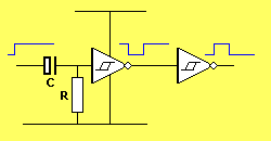
To invert the output, add an inverter:
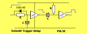
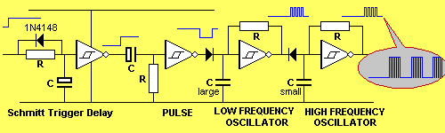
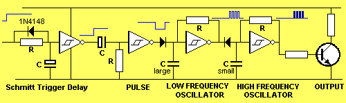
To produce a pulse after a delay, the following circuit is required:
The following circuit produces a tone during the HIGH period. When the output of the second inverter is HIGH, it places a high on the input of the third inverter, via the diode.
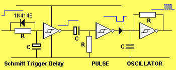
The oscillator above can be set to produce a 100Hz tone and this can activate a 2kHz oscillator to produce a 2-tone output. A "jamming diode" is needed between the third and fourth gates to allow the high-frequency oscillator to operate when the output of the low-frequency oscillator is HIGH.
The output can be buffered with a transistor:
Extending the action of a push button
The action of a push button can be extended by adding the following circuit:
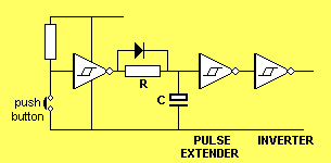
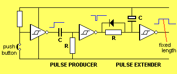
To produce a pulse of constant length, (no matter how long the button is pressed), the following circuit is needed:
GATING
Gating is the action of preventing or allowing a signal to pass though a circuit.
In the following circuit, buttons "A" and "B" are gated to allow the oscillator to produce an output.
The first two inverters form an "OR-gate." When the output of the gate is HIGH it allows the oscillator to operate.
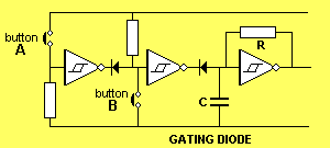
The second diode is called the gating diode. When the output of the second inverter is LOW, the capacitor is prevented from charging as the diode will not allow it to charge higher than 0.7v, and thus the oscillator does not operate.
When the output of the second inverter is HIGH, the capacitor is allowed to charge and discharge and thus oscillator will produce an output.
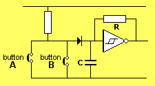
If the push buttons can be placed together, the circuit can be simplified to:
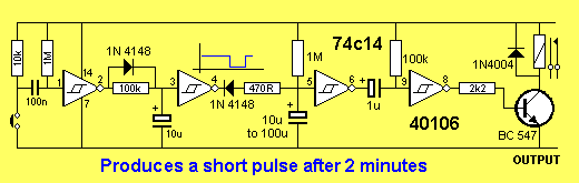
2 MINUTE TIMER
Some of the features we have discussed have been incorporated into the following circuit. The relay is energized for a short time, 2 minutes after the push-button is pressed. The push-button produces a brief LOW on pin 1, no matter how long it is pushed and this produces a pulse of constant length via the three components between pin 2 and 3.
This pulse is long enough to fully discharge the 100u timing electrolytic on pin 5.
The 100k and electrolytic between pins 6 and 9 are designed to produce a brief pulse to energize the relay.
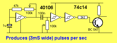
The 74c14 can be used for lots of different circuits. In the following design, the output produces 3mS pulses every second. The circuit is adjustable to a wide range of requirements.
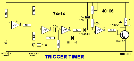
TRIGGER TIMER
The next design interfaces a "Normally Open" and "Normally Closed" switch to a delay circuit.
The feedback diode from the output prevents the inputs re-triggering the timer (during the delay period) the so that a device such as a motor, globe or voice chip can be activated for a set period of time.