FLASHER CIRCUITS |
Basic Electronics Course
Page 83
This page comes from our
Basic
Electronics
Course
It is so important, we have
added it to the
FREE section.
The complete BEC is in the
subscription section
Some circuits in this discussion are available from
Talking Electronics as kits.
(or this link for the web:
Talking Electronics)
All the circuits can be built on our
Matrix Boards. (or this
link for the web: Matrix Boards)
 15 holes x 40 holes $2.95 or: 15 holes x 40 holes |
 24 holes x 25 holes $3.60 or: 24 holes x 25 holes |
|
Each hole in the Matrix Boards above has a circular tinned-copper land and the
components are joined with fine tinned-copper wire. These boards are ideal for creating a project that can then be designed on CAD, using the same layout and you will be sure it will work. If you think you can make a perfect CAD board without firstly creating a prototype, you are either an "expert" or fooling yourself. You must make a prototype to check the performance of anything before launching into a final design. That's why we use MATRIX BOARDS ourselves. It's almost 100% guarantee of success. (or this link: MATRIX BOARDS) Place the components on the top of the board and solder the leads to the lands. The boards can also be used "up-side-down" but this is only for experimenting, when components need to be added and removed until the circuit is operating perfectly. |
|
![]()
Flashing circuits are very interesting. They grab your attention and can be
used in many applications.
They consume very
little energy and some circuits use a single cell that can last as long as 12 months.
You can flash globes, LEDs and pulse all types of devices such as motors,
solenoids and piezo diaphragms.
In this discussion we will cover a number of interesting "oscillator circuits."
They can be adapted for other applications - but to do this you
have to know how they work. This is not easy as most of them are quite complex. In fact oscillator circuits are one of the most
difficult circuits to understand. But if you read the text, everything
will become clear.
But before we do, let's look at a red Flashing LED as a SURFACE MOUNT
component:
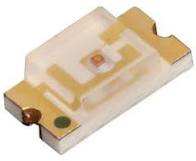
The oscillator inside the case is so small, it cannot be seen.
These devices are the same price as an ordinary surface mount LED and need
no other components. They will operate from 3v to 6v and have an internal
dropper-resistor.
The flash rate is about 1- 2 Hz and are available in red, green, blue and
white.
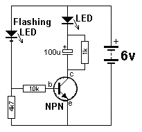
You can also get 3mm LEDs red, green, blue flashing and random flashing and
flickering orange LEDs. These are all available on eBay. Most of them work
on 3v to 7v and take about 10mA to 20mA. You can connect a piezo diaphragm
across them and listen to the oscillator "clocking."
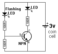
You can use them to illuminate a brighter LED with the following single
transistor circuit. The second circuit operates on 3v from a coin cell.
However, if you want to know how to design a LED Flasher Circuit, this article
will get you started.
Flasher circuits have developed over a long period of time, with many of the
earlier designs proving to be unreliable. One of the earlier successful designs
is discussed in our article,
Spot This Mistake P4
(or use this link for the web: P4).
The first circuit we will cover is the first project you should build, it is:
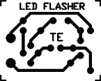
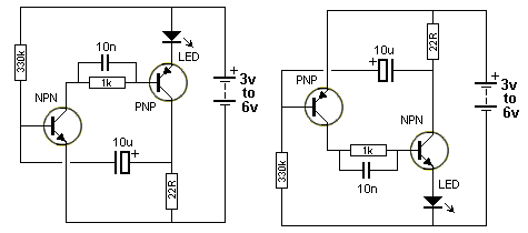
THE LED FLASHER
K-LF1 $3.10
This is a very simple project
using a printed circuit board and 8 components. It will flash an ordinary 3mm or
5mm (1/8" or 1/4") LED at a rate of about one flash per second.
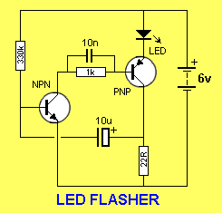 |
PARTS LIST 1 - 22R 1 - 1k 1 - 330k 1 - 10n 1 - 10u 16v electrolytic 1 - BC 547 - NPN 1 - BC 557 - PNP 1 - 1/4" (5mm) red LED 1 - LED FLASHER PC |
A complete kit for this project is
available from Talking
Electronics. (or:
Talking Electronics)
The circuit has a couple of advantages over a flashing LED you
can buy as an individual item. It pulses it with a higher peak
current to give a brighter illumination and consumes less average
current. This means it will work for a long time
on an almost flat battery and cost nothing to run. It can be used
for battery equipment to indicate the power is ON or as an ALARM ON
indicator.
You can use a super-bright LED and get a really bright flash, or an ordinary
green, orange or yellow LED to get something better than a flashing red LED.
 |
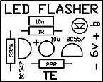 |
THE CIRCUIT
This circuit works on the basis of a high-gain amplifier being driven into saturation (fully turned-on), firstly by the very small amount of current delivered by a high-value resistor and then from energy stored in an electrolytic.
When the energy from the electrolytic has been fully delivered, it cannot keep the amplifier fully turned on and it turns off slightly. This action removes the "turn-on" effect from the electrolytic and the amplifier begins to turn off. This action continues until the amplifier is fully turned off and is kept in the off state while the electrolytic begins to charge. The off-state is very long and the on-state is very short. This is how the LED produces a brief flash.
Here is the technical description of the operation of the circuit:
When the supply is connected, both transistors are off and the electrolytic charges via the 330k resistor and 22R. When the voltage on the base of Q1 rises to about .6v, the transistor begins to turn on and the resistance between its collector-emitter terminals is reduced. This allows current to flow in the collector-emitter circuit and Q2 is turned on via the 1k resistor. The 10n reduces the effect (the resistance) of the 1k resistor. Q2 conducts and the LED is illuminated. The current through the LED is limited by the 22R resistor and at this point in the cycle a voltage is developed across the 22R. The negative end of the electrolytic is `jacked up' by this voltage and the positive end pushes the charge on the electrolytic into the base of Q1 to turn it on even harder. In a very short time all the energy in the electrolytic has been delivered to Q1 and it cannot hold Q1 ON any longer. The transistor turns off slightly and this has the effect of turning off Q2 a small amount. The LED begins to turn off and the voltage across the 22R reduces. The negative lead of the electro drops a small amount and so does the positive lead. This action continues around the circuit until Q1 is fully turned off. This turns off Q2 and the LED is extinguished. The cycle starts again by the 10u charging. The charge-time is considerably longer than the discharge time and this gives the LED a very brief flash.
CONSTRUCTION
All the parts mount on a small PC board and it has an overlay (all our boards have overlays) as shown in the diagram below:
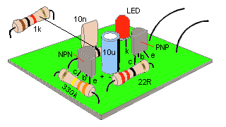
This makes construction very easy and all you have to do is bend
the leads of the components so they pass down the holes in the board. The
resistor leads are bent to 90° and are
pushed
all the way down so they rest on the board. The leads are then bent
slightly to hold them in place while the leads are soldered.
Fit the three resistors in this way and you are ready for the two
capacitors. The 10n can be fitted either way around but the 10u
electrolytic must be fitted so the positive lead goes down the hole marked with
a "+." The positive lead is the shorter of the two
leads
and the
negative
lead is marked on the side of the body of the component with a "
—"
Refer to the
diagram above for the identification of the cathode lead. Keep the LED above the board so
it can be clearly seen. Solder a short length of red and black wire to the board
and to 4 cells to complete the project. You can use almost any old cells for
the 6v supply and let the LED FLASHER use them up completely.
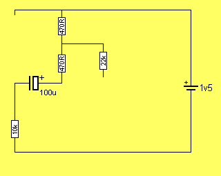
The next circuit replaces a flasher chip. These are no longer available but
many circuits use them. Here's the alternative:
When power is applied, the 100u is uncharged and zero voltage is across its
terminals.
The voltage on the top of the 10k resistor actually goes about 1v below the 0v
rail and makes the 10k dip down as shown in the diagram above.
There is one very important requirement when designing an oscillator.
The two transistors are next and it is important not to mistake the
PNP for the NPN. They both look identical. Check with the parts list
for the types you have been given in the kit. Fit the leads down the
holes so that the transistor is 2mm (1/8") from the board and
bend the leads slightly so it does not fall out when the board is
turned over and soldered. Finally the LED is fitted to the board.
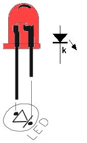
Fitting the LED
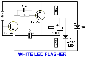
1.5v LED FLASHER
The next circuit flashes a LED and uses a 1.5v supply. The LED does
not turn on via the 1k resistor because the characteristic voltage of a LED
is between 1.7v and 2.3v, (depending on the colour). It turns on when
the 100u is "jacked up" by the collector of the BC557.
The circuit is a charge-pump design. This is where a capacitor
(electrolytic) is allowed to charge and is then raised higher and allowed to
discharge into a load. The load sees a voltage that can be higher than the
supply.
This is the case with this circuit.
The two transistors operate as a high-gain amplifier with the output being
the 47R. The cycle starts with the first transistor being turned on via the
100k. This action also charges the 10u until 0.75v appears on the base of
the transistor.
This turns on the second transistor and the negative end of the 10u is
raised when the BC557 turns on. This raises the positive end of the 10u and
the first transistor turns on even more. This action continues until the
first transistor is fully turned on and the BC557 is fully turned on. The
voltage across the collector-emitter terminals of the BC557 will be small
and about 1v will appear across the 47R. This voltage "jacks up" the 100u
and since it is fully charged via the 1k resistor, it will present a voltage
of about 2.5v to the LED. Any voltage over 1.7v will turn on a red LED and a
green LED will turn on at 2.3v. The energy in the 100u is now passed to the
LED to illuminate it.
The flash is very brief due to the operation of the two-transistor
amplifier. Although the energy in the 100u will produce a brief flash, the
timing of the two transistor circuit is even faster and it provides the
duration.
The actual duration of the flash depends on the time the two transistor
amplifier can be in a fully turned-on state. This is governed by the
charging of the 10u electrolytic.
When the base of the first transistor sees 0.7v, the two transistors start
to turn on by a process called REGENERATION. This is explained further in
our article: REGENERATION, in
Circuit Tricks.
Regeneration is a condition where a circuit turns on more and more without
any external assistance.
And this is what happens in this circuit.
The 10u is "jacked up" by the BC557 turning on and it delivers a current to
the base of the BC547. Initially it delivers its energy to the base but very
soon is is higher than 0.7v and it is fully discharged. The electrolytic now
starts to charge in the reverse direction and this process continues to keep
the BC 547 turned on. It charges very quickly in the reverse direction as
the charging path is the emitter-collector junction of the BC557 and
base-emitter junction of the BC547. When it is nearly charged, the
current-flow reduces and this turns off the BC547 very slightly. This turns
off the BC557 slightly and the 10u is "lowered." This puts less "turn-on" on
the BC547 and the two transistors start to turn off very quickly.
The 10u is now charged in the reverse direction and a negative voltage is
presented to the base of the first transistor. This voltage is is gradually
reduced by the electrolytic charging via the 100k and that's why the circuit
has a very long off cycle.
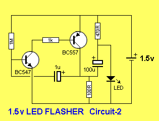
Two circuits are shown. They use slightly different components to produce
the same results.
The only critical value is the 100R. The circuit will not work with a value
higher than about 150R. It needs a low value so the BC557 transistor is
turned on to a high level before a voltage is developed across the 100R. If
the value is too high, a voltage will be developed across this resistor when
the BC557 is turned on a small amount and this voltage will be sent to the
BC547 to turn it on too. The two transistor will sit in a conditions that
they are both turned on and the circuit will freeze.
The circuit has to function such that the BC547 is turned on to its maximum
when the electrolytic is pulled HIGH. This transistor will now be turned on
by the current delivered by the 100k (or 1M) plus the charging current of
the electrolytic. As the electrolytic charges, the current into the
base of the BC547 will fall and the transistor will turn off slightly. This
slight turn-off must be passed to the BC557 to turn it off slightly too and
lower the "turn-on" effect of the electrolytic. It is the 47R (or 100R) that
is pulling the electrolytic down to the 0v rail and if this resistor does
not have sufficient "pull-down" effect, the cycle will not continue. When
this resistor has a low value, the BC557 must deliver a high current and it
must be turned on via a proportionally high current into the base. This
current comes from the BC547 and it needs a proportionally high current into
its base to provide this condition. We are only talking about fractions of
milliamps and microamps, but these conditions must be met for the circuit to
work. 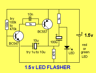
THE LM 3090 FLASHER CHIP
The LM3909 flasher chip has been discontinued for a number of years and the following circuit can take its
place: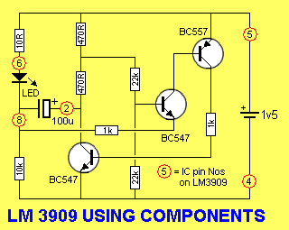
It is charged via the two 470R resistors and 10k resistor and these three
resistors create a voltage divider across the 1.5v supply such that the voltage
on the top of the 10k resistor is
about 1.4v
This makes the emitter of the middle transistor about 1.4v and thus it is not
turned on.
The BC 557 is also not turned on and the first transistor is also not turned
on.
As the 100u charges, the voltage across the 10k resistor decreases and the
middle transistor begins to turn on.
This turns on the BC 557 and the first transistor begins to turn on very
quickly and very soon it is fully turned on.
This effect brings the positive of the 100u towards the 0v rail and the best
way to see how the voltage across the electrolytic adds to the 1.5v supply to
produce a voltage above 2v, is to refer to the following diagram: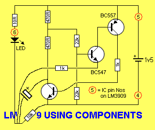
The timing capacitor must be discharged.
In other words the circuit must create a state that discharges the
capacitor and remains in that state until the capacitor is fully or almost
fully discharged.
If it is not discharged, it cannot be charged again!
So, let's start at the beginning:
The analysis of the circuit starts at the base of the middle transistor. The voltage at this point is approx half the supply voltage when the circuit is turned on as no transistor is conducting and the electrolytic is discharged.
Since the voltage on the circuit is only 1.5v, the LED is a very high impedance at this voltage as it does not activate until the voltage is above its characteristic voltage of approx 1.7v.
The only components that are effectively "in circuit" are shown in the following diagram, and the electrolytic begins to charge:
When the circuit is first tuned on, the electrolytic has zero voltage across
it and the 10k and 470R resistors are in series. About 0.13v is across the two
470R resistors and 1.37v is across the 10k resistor.
As the electrolytic charges to about 1.2v, the middle
transistor begins to turn ON as the voltage on the top of the 10k resistor
drops from 1.37v to about .17v.
Charging the electrolytic
As the electrolytic charges, the voltage across the 10k reduces.
The following animation shows how the voltage across the 10k changes: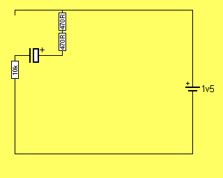
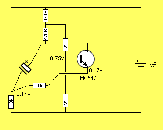
The voltage between the base and emitter of the transistor is 0.58v and the
transistor begins to turn on.
The transistor used in the prototype turned on at 0.38v and this is the secret
behind the circuit operating down to a supply voltage of about 0.8v
In the diagram below, the middle transistor is turned on slightly and this
turns on the third transistor. The third transistor turns on the first
transistor.
The first transistor pulls the lower 470R resistor towards the 0v rail and
the positive end of the electrolytic. The negative end is also pulled down as
shown in the following animation:
Here is the clever part:
The FM transmitter section above operates continually from the 1.5v and the
"flasher chip" provides a slight interruption to create a "beep" on the
airwaves which is really the transmitter shifting off frequency and the
carrier being lost. It does not use the "jacked-up voltage" feature of the
chip.
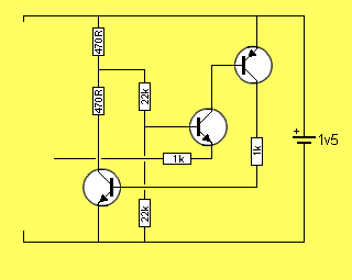
All the transistors are
turned ON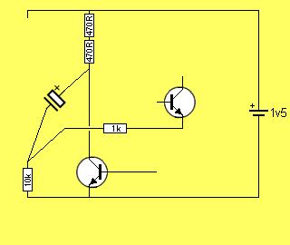
As the electrolytic charges, the emitter of the middle transistor is being pulled down
and the base is
being pulled down at half the rate. This means the voltage between the base
and emitter is widening and the transistor is being turned on MORE.
This is called REGENERATIVE ACTION. The action continues until the
first transistor is fully turned ON. 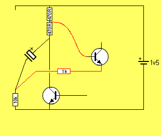
Here is a circuit using the LM 3909: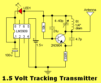
If a load other than a LED is connected to the circuit, the electrolytic will
not charge.
The circuit relies on the fact that the LED is an "open-circuit" when the
supply voltage is below the characteristic voltage of the LED (approx 1.7v).
The circuit, however, can be used as an oscillator to drive other loads
providing the LED and electrolytic are retained as they provide the "timing
component" and "load."
This makes the circuit very wasteful with current if required for other
applications.
There are other circuits more suitable, as you will see.
Next, we have the astable multivibrator, or FLIP FLOP [pronounced (h)ay
stable] - meaning it has unstable states. In this case, two unstable states.
This is the simplest circuit capable of alternately flashing two LEDs. The
flash-rate is determined by the two 10k resistors and two 100u electrolytics.
The flash-rate can be increased or decreased and one LED can be made to flash
brighter by altering the 4 components.
The operation of the circuit is fully discussed in the Basic Electronics
Course P17 & P19
(subscription needed)
and in
5 Projects
P16. (use this link for the web:
5 Projects)
It can be purchased as one of the kits in
5 Projects. (use this link
for the web: 5 Projects)
This circuit does not have the advantage of the two described
above. It does not pulse the LED with a high current for a short period of
time and thus it is not as efficient as the two above. When a LED is pulsed
with a high current for a very short period of time, the output is almost as
bright as a constant, lower-current. 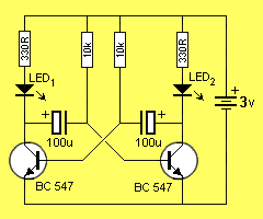
Here are some Flashing LED circuits from "200 Transistor Circuits' eBook. The first 4 circuits show how to change an NPN transistor for PNP.
UNCONVENTIONAL CIRCUITS:
The following circuit converts 1.5v to a voltage
that is higher than the reverse break-down voltage of the emitter-collector
junction of the BC547. When this voltage is reached the junction breaks-down
and creates a low voltage across it. This allows the voltage on the 100u to
pass to the white LED and create a flash. The voltage across the 100u
drops and the junction comes out of conduction and the cycle repeats.
The next circuit uses the same
"Junction Breakdown" phenomenon but this time the high
voltage is supplied by a 12v to 20v battery.
The circuit above is very unreliable and only works with some transistors. The
voltage is very important. It must be high enough to cause the junction(s)
between the emitter and collector leads to breakdown.
The following simple circuit flashes a globe at a
rate according to the value of the 180R and 2200u electrolytic.
All transistors have a single junction or two junctions between each pair of leads. They
are
called a "PN" junction or a PNP junction or an NPN junction - depending on
which leads are selected. The junctions between each pair of leads behave
differently, however the junction(s) we are interested in, is between
the collector and emitter leads.
When a voltage is applied to these leads in the reverse direction, an
unusual thing happens.
As the voltage is increased, the junction suddenly breaks
down and a high current will flow , according to the energy available from
the electrolytic. This occurs at a voltage of between
12v and 20v, (some transistors will require a higher voltage) depending on the type of transistor and the manufacturer.
When the voltage across the leads falls, the current stops.
In other words, the resistance between the two leads decreases when the
voltage rises to between 12v and 20v (and the voltage across the two leads
is about 0.5v and this is a characteristic of the junction). When the
supply-voltage drops, the
junction-resistance increases and the electrolytic charges.
This feature can be used to flash a LED as shown in the following
diagram:
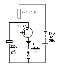
Flasher circuit using "Junction
Breakdown"
The flash-rate will depend on the value of the top resistor and the
electrolytic and also the voltage at which the transistor break-down.
The circuit consumes less than 1mA and the 100R prevents a high current
flowing through the LED (from the electrolytic). Without the 100R, the LED
is destroyed instantly.
The circuit is a very good demonstration of breakdown
but due to the high supply voltage needed, it is not a practical design. The
previous circuit should be used.
LAMP FLASHERS
The following circuits will flash a car globe for a Warning
Beacon.
It uses two Darlington transistor in a flip-flop circuit. The
layout must be kept "tight" (thick wires) to be sure it will oscillate.
A complete kits of parts and PC board costs $5.00 plus postage from: Talking
Electronics. Email
HERE for
details.
![]()
Warning Beacon
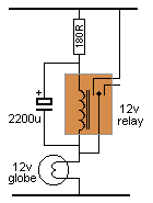
Simple Flasher
The Flasher can alternately flash 2 globes as shown in the following circuit. You will need to adjust the value of the components to get an equal flash-rate for the two lamps. It is a mechanical equivalent to the flip-flop circuit above.
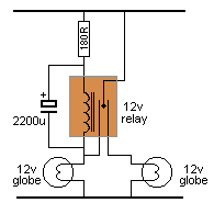
Dual
Flasher
7-10-2020