SPOT
Biasing Resistors
The resistors have values 1k, 10k and 47k:
When testing a transistor with in-built resistors, you will get a "false"
reading when measuring across the leads of the transistor as the resistor will
change the value. This is a feature you need to be aware of.
The 200k will damage the discharge transistor inside the chip when it is turned to zero
ohms.
A "Stop Resistor" prevents the resistance of a potentiometer going to
zero ohms. In some cases a very low resistance will cause a high current to
flow and damage either the potentiometer and/or other circuit components. You
must always check this when fitting a "pot."
Tracking Transmitter
The emitter of the transistor should have a resistor so that the signal through
the 4p7 will modify the voltage on the emitter and make the transistor
oscillate.
If the resistor is omitted, the
circuit may work due to the fact that the LM3909 flasher chip has a high
impedance on its pins but the output will certainly be reduced.
The collector-emitter junction of the PNP transistor
and base-emitter junction of the NPN transistor are connected directly across
the power supply.
Both circuits have a number of
defects:
The revised circuit has one mistake. It does not work!
Here is another LED FLASHER circuit:
This circuit has a problem. It does not work when the voltage drops a small
amount and will not work on 9v. It is very voltage-critical.
The next discussion is not a mistake but "how to go about it."
It is a 6-leaded surface-mount chip
1.13mm X .71mm with "D2" identification.
UM 3561 4-Sound IC
The problem lies in the connection of the first transistor to the positive
rail. As the voltage on pin 3 rises, the two transistors begin to turn on
when the voltage on the base of the first transistor is 1.3v.
THE MISTAKES!
Page 4
Page 1
Page 2
Page 3 ____
Page 5
Page 6
Page 7
INDEX
![]()
The next discussion is not a mistake but an item that needs careful
attention.
A range of surface-mount transistors are appearing on the market with in-built
biasing resistors.
While this may sound like a good idea, it presents a lot of problems.
Biasing a transistor is a very critical factor and depends on the current to be
delivered by the transistor and the quiescent current you want the circuit to
take.
The bias-value can range from a few "k" to more than "1M."
You don't want to be "dictated to" by a supplier of components. The
range of values offered by the supplier in this case is very limited.
But the major problem with using transistors with built-in bias resistors is the cost.
Surface-mount devices are only available on reels of 3,000 and if the wrong
value is chosen or you need to change a particular value, a reel is wasted.
The wonderful part of electronics is its universality.
Electronics is made up of interchangeable components that are common throughout
the world
and that's why it has flourished and expanded.
We have already made electronics universal, so let's not ruin the concept
by individualizing basic components.
When designing a project, make a point of not using specialised components, unless
absolutely necessary.
It will only back-fire in the long run.
Your products will be harder to service and less-likely to be recommended.
![]()
.gif)
.gif)
.gif)
.gif)
.gif)
.gif)
.gif)
.gif)
Stop Resistor
A 555 circuit posted on an "electronics forum" had the following mistake: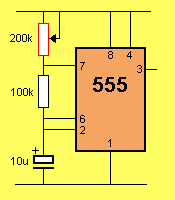
The circuit needs a "stop resistor" as shown in the diagram below: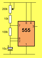
Use a "stop resistor"
The diagram below shows the internal structure of a 555. Pin 7 is connected
to the collector of a transistor and must not be connected directly to the positive
rail. If the collector of the transistor is connected to the positive rail, it
will conduct a very high current when it is turned on. It is turned on every
time the output pin (pin 3) is taken HIGH.
To learn about the 555, see
our 3-page article on the CD,
P1
P2
P3 or
P1 in our Projects section.
On the CD, see the TEST on the 555. On
the website the TEST is
HERE.
This 555 article is the most comprehensive you will find. It includes a program
to show the frequency of oscillation for any value of resistance and
capacitance and the HIGH and LOW times. 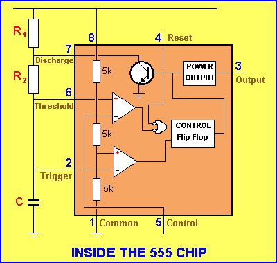
The next discussion comes from the web.
The circuit is very well designed but a small improvement can be made. 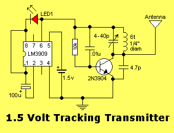
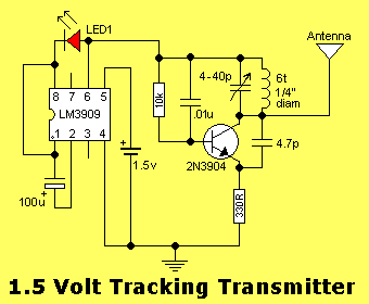
The way the transistor gets its feedback to maintain oscillation, is as
follows:
The PARALLEL TUNED CIRCUIT, made up of the variable 40p trimmer and coil
creates a waveform and this is passed through the 4p7 to the emitter of the
transistor. The base is held rigid by the 10n capacitor and the emitter "moves
up and down."
There are two ways to turn a transistor on.
One is to raise the voltage on the base, while keeping the emitter fixed and
the other is to change the voltage-level on the emitter, while keeping the base
fixed.
The 330R keeps the emitter away from "ground" so it can be injected with a
signal (voltage) by the 4p7.
The LM 3909 is no longer manufactured and a substitute circuit is shown in our
Flasher Circuits
article.
The next mistake is similar to one of the first items we discussed in this
chapter.
It's the mistake of allowing the junctions of transistors to be connected
directly across the power supply. The following circuit contains the fault: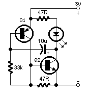
The faulty circuit
When both transistors are turned ON (when the LED is illuminated) they form a
voltage drop that can be as low as 0.2v for the
collector-emitter junction and 0.7v for the base-emitter junction. This is
lower than the 3v supply and will cause a very high current to flow.
The end result is about 80% of the current taken by the circuit flows though the junctions and only
20% through the LED!
This circuit is very wasteful.
By adding a 100R resistor as shown below, the current drops to 10% of the
original!
This is only a "proving-point." It does not alter the fact that the circuit is
of poor design.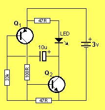
The improved circuit
1. They will not operate on weak batteries.
2.
The bottom 47R represents a low value of resistance and indicates waste of
energy. (The
top 47R is needed as a current-limiting device for the LED and cannot be
changed or omitted.)
The circuit
should be re-designed and the bottom 47R replaced with a higher value.
Here is the reply from the author of the original circuit: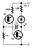
The author says it works. But it did not work for me.
Who's right? Obviously I am.
A circuit must work and must be reliable for almost any type of
similar transistor. It must also be reliable for component values slightly different
to those
specified.
That's the art of making a reliable circuit. It must work under a wide range of
conditions.
Obviously this circuit is too fiddly.
The answer is to re-arrange the components: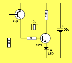
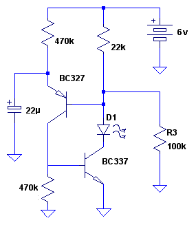
The flash-rate is very low @ 9sec per flash for 22u and 4 seconds per flash
for 10u.
However it has one advantage. The current consumption is very low at 50
microamps.
The energy from the electrolytic is delivered to the LED to create a fairly
bright flash and there are no losses in a load resistor for the LED.
The 100k and 22k resistors form a voltage-divider to set the point at which
the circuit turns on.
The 22u must charge to a point that is 0.6v higher than the mid point of the
voltage divider and this creates the timing for the flash as well as the
brightness.
If you have a reliable supply voltage, this circuit is suitable. If you are
trying to use the last of a 6v set of cells, this circuit will stop when the
voltage reaches about 5v.
See our Flasher Circuits
article for more circuits.
A readers sent a request to identify a surface-mount component: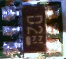
The letter "D" does not mean it is a diode and the 6 leads do not mean
all the pins are used.
After searching through surface-mount identification lists, the reader was
no further advanced. He spent more than 8 hours trying to find a answer.
At this point things become desperate.
You need to advance, so here's my suggestion:
The next step is try and work out if the product is very new or not. This may
mean the chip is a "new style" device containing transistors, resistors and
diodes in a mini-circuit arrangement.
Next, you have to work out if it is faulty and if you want to risk removing it
from the board.
Before you remove it, take a resistance reading across each of the pins in both
directions. This will be a lot of readings so make a number of drawings and fill
in the details.
To remove the chip you will need a surface-mount removal tool or a fine
soldering iron, some fine solder, long-nose pliers and de-solder wick.
Start by soldering each pin with fresh solder. Only solder one pin at a time
and wait for the chip to cool down.
This cleans up the joints and makes removal of the solder very quick and easy in
the next step.
Use a hot iron and suck up the solder from one pin at a time with a new section
of de-solder
wick.
Continue with the other pins.
You will now need to put a very fine jewelers screwdriver under the end of the
chip and exert a small amount of lifting pressure while running the hot
soldering iron down one side of the chip. One side of the chip will then lift
off the board. Grip the chip with fine pliers and run the soldering iron down
the other side.
Measuring the chip with a multimeter will not tell you anything. You do now
know what's inside it. But measuring it will help in the next step.
Trace out the circuit surrounding the chip.
Sometimes the external components will help you work out what's inside.
You can then solder components onto the lands and create the circuit as a
"bird's nest" to see if it works.
This may be a lot of work, but you have to do something.
If you go to our Chip Data
eBook, you will find outline diagrams for many of the chips as well as the new
"hybrid" chips and links to the web.
From this you will get some idea of what to expect inside the chip.
It's just a matter of duplicating this and see if the circuit works.
Now we have a mistake that has been covered before. See if you can find the
problem: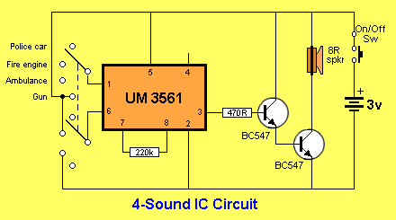
This voltage will not increase but as the voltage on pin 3 increases, the
current through the 470R resistor will increase and the first transistor
will allow at least 100 times this current to flow between the
collector-emitter terminals and into the base of the second transistor.
Using Ohms Law, this comes to 3mA through the 470R resistor and up to 300mA
into the base of the second transistor. This is clearly a waste of current
and may damage the transistor.
The solution is to add a current-limiting resistor in the collector of the
first transistor as shown in the diagram below: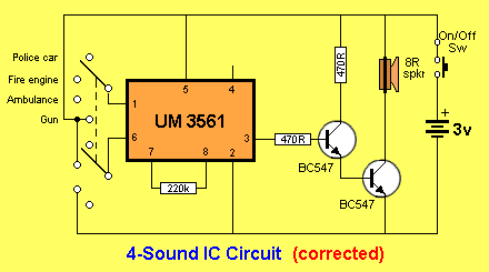
The next fault comes from the same circuit we covered above. It is the
turn-on section.
When the light-beam is broken, the infra-red receiver transistor has a high
resistance and
the turn-on transistor is pulled high via the 33k and top 10k resistors.
But there is a fault in the turn-on section. Can you spot it?
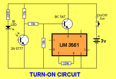
The chip will not see a "turn-on" voltage. The
voltage-divider, made up of the 33k, 10k and bottom 10k resistors will put a voltage of 0.56v
on the base of the BC 547 transistor. The voltage drop of 0.6v between the
base and emitter will result in zero volts reaching the chip.
The lower 10k is causing the problem. It is not needed.
How do you work out the voltage that will appear on the base of the BC 547?
We firstly assume the two transistors are not putting any load on the
circuit. In other words, they are high-impedance (not turned on) for this
part of the discussion.
The circuit becomes as shown in the next diagram:
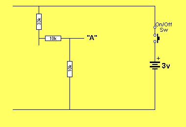
The total resistance of the network is: 33k + 10k
+ 10k = 53k
The voltage across the network is 3v.
The voltage across each 1k = 3/53 = 0.0566v
The voltage across the lower 10k = 0.566v
As we have mentioned above, the base-emitter voltage of the BC 547 will
remove this voltage and the chip will see 0v.
The next point to note is purpose of the upper 10k.
It serves no purpose at all.
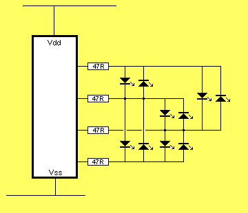
The corrected circuit is shown below:
Here is the improved circuit diagram:
In the diagram above, it is obvious that the LEDs are in pairs, with one LED
connected in the opposite direction to the other. 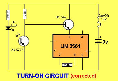
The next item is not exactly a mistake, but an
improvement to a layout.
Circuit diagrams should always be laid out so they give an immediate
indication of how the circuit works.
The following circuit looks very neat but it is more complex than it should be.
The LEDs are actually connected in opposite directions to the 4 drive-lines of a
micro, but this is not obvious.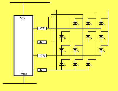
Each pair of LEDs is connected to two output lines so that by reversing the
polarity of the lines, any LED can be individually accessed.