SPOT
THE MISTAKES!
Page 2
Page 1 ___
Page 3
Page 4
Page 5
Page 6
Page 7
INDEX
![]()
THE KEY-HOLE LIGHT
The possible reasoning behind the circuit goes
something like this: The first transistor is turned on by the electrolytic charging via the
820k resistor and this holds the other two transistors off.
The 100k resistor serves two purposes. Firstly it limits
the current into the base of the first transistor when the switch is closed and it allows the
positive side of the electrolytic to charge to full rail voltage.
The way the circuit works is the Light Dependent Resistor robs the SCR of gate voltage when
the light is bright. This is because the resistance across the LDR (in bright light) is low.
At first glance you may accept
these figures but let's look into the reality of the situation. No values of components were
given on the diagram and this is possibly why the writer made the mistake. He obviously did not
try the circuit himself - which is a gross oversight.
When the base is shorted to the emitter, the transistor turns off and it effectively comes out
of circuit.
The basic fault in the circuit is the placement of the buzzer. It is in the emitter of the
transistor and this makes the transistor an emitter follower.
If the water being detected has a lot of dissolved salts, the resistance across the sensor
plate will be very low and you may require a resistor to limit the base current to prevent the
transistor being damaged.
Before we look at the
faults, let's talk about the development of circuits that flash one or more Light Emitting
Diodes. In the early days a number of circuits were designed to flash a small globe or
alternately flash two globes. These circuits were either a multivibrator or a positive
feedback amplifier.
I built it twice, without any
luck! It is supposed to produce a siren sound but after putting it together, all I got was a
click from the speaker after about 5 seconds.
It comes from Charles Rener, of Starlight Electronics. Charles
is constantly working with oscillators to drive his electroluminescent displays, so he knows a
lot about oscillators. He thought it would be good for this series. We are utilizing the characteristic voltage drop of 1.7v per LED to
connect a point on the oscillator to a point on the output stage that has a difference in
voltage of about 3.4v.
If the output of the saw-tooth oscillator is connected directly to the base of the PNP driver
transistor, the transistor will be turned on ALL THE TIME.
WHY THE 56R?
It consists of a Hall effect device
(contained within the dotted rectangle) with leads labelled 1, 2 and 3. Two external
transistors connect the hall device to a load.
The circuit now changes from a poor design to one that cannot be criticised.
500 MILLIAMPS!
The text accompanying the circuit read as follows: There are two major mistakes in the circuit. Apart from the danger of
over-driving the LEDs, the circuit is actually incapable of delivering the
current suggested in the article. The 12R resistors in series with each LED
will allow nearly 800mA to flow when the transistor is turned on. Fortunately
for the designer of the circuit, the maximum current capability for a BC547 is
only about 100mA and so the maximum current through each LED will be within the
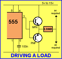
range we stated above. I found the next mistake in a 555 Projects book. This is a
glaring example of the writer not knowing the in's and out's of the chip. The
555 has a maximum output voltage that is 1.7v LESS than rail voltage. This is a
very poor feature and is one of the reasons I do not recommend using this chip
for anything other than the simplest 12v project.
The 555 loses 1.7v on the output pin, why fit an emitter-follower to the output
and lose another 0.7v? For a 12v supply, the load voltage will be a maximum of
9.6v The solution is to connect a common-emitter stage and deliver
11.6v to the load.
The next circuit (shown in Fig: 10) has two mistakes. One of them was so serious it folded the company! The company marketed the device as a key-hole light to illuminate a key-hole for 6 seconds then turn off. It was a brilliant idea (no pun intended) and they sold thousands of units. But a problem arose. The batteries did not last 2 years as stated on the package. They only lasted
2-3 weeks!
Something must be wrong, they thought. The batteries must be faulty. But after careful testing,
the circuit was found to be at fault!
What a disaster. The problem was the circuit did not power down to zero. It took 60uA in the off condition and even though this may not sound very much current, the combination of current and time was sufficient to completely flatten two AAA cells in 3 weeks.
The circuit was obviously designed by someone who knew absolutely nothing about electronics as it had been designed incorrectly.
The original circuit is shown in fig: 10
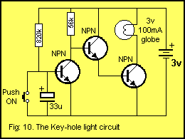
But the current required to keep the electrolytic charged plus that flowing through the 56k
load resistor to keep the other two transistors off, is wasted current and when designing a
battery operated device like this you have to think very carefully about the "shut-down"
current.
By a slight re-arrangement of the parts, and the omission of one transistor, the same 6 second
delay can be obtained and the current will drop to less than 1uA when it is not being used.
This allows the batteries to last up to 50 times longer and a failed product turns into a
success.
Now you can see why it's so important to learn the basics of electronics.
The rise or fall of a company can hinge on knowing a little about circuit design - especially
in this case.
Our improved design is shown in fig 11.
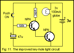
This gives the electrolytic more energy so the time delay can be as long as possible. The
energy from the 47u is then fed into the first transistor via the 100k to keep it turned on for
as long as possible.
As the energy flows out of the 47u, the voltage across it decreases and when it drops to about
1.4v, the two transistors (in Darlington mode) cannot be kept on any longer and the lamp begins
to dim. Eventually it goes out completely.
To make sure the current in the "off" mode drops to a very low level (about 1uA) it is
important that the voltage on the electrolytic is less than 1.4v.
To make sure this happens you could add a 1M bleed resistor across the 47u, but tests on the
circuit we built, show the shut-down current falls to below 1uA and this is acceptable for long
battery life.
These changes took only a few minutes to re-design and they could save a company thousands of
dollars.
THE NIGHT-LITE
Another device that needs slight improvement is the night-lite shown in the
diagram below. It turns off when the ambient
light in the room reaches a certain level. But the set of night-lites I bought did not go off
at all because the light level in the room was not sufficient to turn off the SCR.
The circuit for this is shown in fig 12.
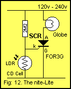
The lamp turns off when the photo resistor (LDR) has a resistance of about 10k. But the light
has to be fairly bright to get the cell to go this low and so we had to think of a solution.
There are three possible solutions. Can you think of a way to fix the problem? Solution 1 is to
buy another, more expensive night lite.
Solution 2 is to increase the 2M2 to 4M7 so that the voltage divider network made up of the
resistor and photocell, will give the gate less voltage at a particular light intensity.
But the simplest answer is to place a 10k resistor across the photo resistor so that it helps
rob the gate of turn-on voltage.
A TRANSISTOR CIRCUIT
Next we come to a transistor circuit from a text book. The author states that if the base is
shorted to the emitter, the voltages will be as shown in fig 13.
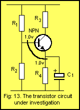
The resistor values in fig 14 are typical and will produce about 1v on the emitter of the
transistor.
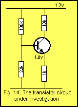
The only remaining components are the 100k in series with the emitter resistor and 22k. The
voltage across the 1k will be 1/100th of 12v or 0.12v and NOT 1v as stated in the text book.
A WATER DETECTOR
Here's another simple circuit with a basic fault in the design.
Fig: 15 shows a water detector using a sensor plate made from a PC board having two
interleaving tracks. The circuit detects water such as the flooding of a basement etc.
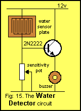
The resistance of the detector plate forms a voltage divider with the 1M sensitivity pot and
the voltage at the junction of these two is passed to the base.
As the resistance of the detector plate decreases, the voltage at the junction increases and
the transistor passes this voltage to the buzzer. When the plate is 1M, for example, the
voltage at the junction will be 4.5v. At this voltage the buzzer will not be very loud. The
plate must reduce to less than 100k to get the maximum voltage possible for the buzzer.
If the buzzer is placed in the collector, it will be louder for the same degree of moisture
detected. In other words the circuit will be more sensitive.
Obviously the circuit needs to be as sensitive as possible so that it can be "turned down" if
necessary. Fig: 16 shows the correct circuit.
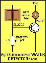
One other minor point. A buzzer is not a very loud device and if you require a loud output, you
should use a piezo sounder. This is a piezo diaphragm with an active circuit that will produce
a very loud output at 9v. It requires very little current (about 15mA) and is ideal for this
purpose.
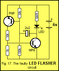
LED FLASHER
Three faults in the next circuit (shown in fig: 17) are fairly technical.
With the development of the Light Emitting Diode, the circuits were re-designed.
An example of the multivibrator is the Robot Man project in Learning Electronics Book-1 and an
example of the positive feedback circuit is the LED Flasher project, also in Learning
Electronics Book-1. Both these circuits are highly reliable. They will operate with almost any
types of transistor and any component values near the ones stated on the circuit diagram. They
are also completely independent of supply voltage. Along with these good designs there were a
number of others that were very tricky to get going. I recall three early designs and have
shown one of them in fig: 17. At a quick glance the circuit appears to work ok but when you
build it up, the 150k resistor is very critical and the flash from the LED is very weak. Once
you get the circuit going, it will cease to function when the battery voltage falls by even a
volt or so. It is simply an unreliable design and that's why it is in the spotlight.
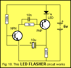
Fortunately, by re-designing the circuit slightly, (as shown in fig: 18),
the LED will produce a brilliant flash and
the circuit is guaranteed start-up every time. That's the way a circuit should be. It should be
completely reliable and guaranteed to work.
AN OSCILLATOR CIRCUIT?
Next we come to a circuit that has me fascinated. It's fig: 19.
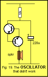
The circuit charges the capacitor via the 10k resistor. When a certain voltage is reached, the
emitter-collector junction of each transistor breaks down and they conduct. This causes the
capacitor to discharge into the speaker.
In theory, the capacitor is supposed to discharge to zero volts and unlock the junctions of the
transistors so the capacitor can start to charge again. But unfortunately about 0.7v remains
across the capacitor and the transistors do not unlock so the cycle halts after one click.
Maybe some types of transistors will work but rather than take the risk, I suggest avoiding
anything that requires fiddly attention to get it going.
Most of the circuits in use today are extremely reliable. This is because they have been
refined from circuits that did not always have reliability. I classify fig: 19 as unreliable
and should be avoided.
A SAWTOOTH WAVEFORM
The next circuit is different. It looks too simple to be an oscillator and you may wonder how
it works. The amazing thing is it DOES work. The only problem is interfacing it to other
building blocks, as we shall see.
The circuit has a couple of problems that don't come to light until it is put together and
tested. That's why we have added it to our list.
The circuit is shown in fig: 20.
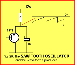
Provided the circuit is supplied with a voltage above 9v, it will produce a sawtooth waveform.
The actual frequency of oscillation depends on the value of the capacitor and resistor in the
'TIMING CIRCUIT.' With 1k and 1u, the frequency is approx 3kHz.
The circuit relies on the fact that a transistor breaks-down or ZENERS when a reverse voltage
is applied between the emitter and collector leads.
For a BC 547 this break-down will occur at about 9v. When the voltage drops below 7v, the
transistor comes out of break-down.
The capacitor across the transistor is part of a Time-Delay circuit to create an interval of
time between 'break-down' and 'non-breakdown.'
The circuit operates as follows: Power is applied and the capacitor charges via the 1k
resistor. When the voltage across the capacitor reaches 9v, the transistor breaks down (as it
is directly across the capacitor). The transistor effectively puts a short across the capacitor
and thus the capacitor discharges through the transistor.
When the voltage across the capacitor falls to about 7v, the transistor comes out of break-down
and the capacitor begins to charge to repeat the cycle.
The first fault in the design lies in the fact that the base lead of the transistor is left
open or floating and has the tendency to pick up noise and affect the frequency of the
oscillator.
But the biggest problem with the circuit is the difficulty to interface it to other building
blocks.
The output has a 2v swing but this swing does not come near either of the rails. It is between
7v and 9v. In other words it is very difficult to DC couple the output to another stage.
Finally, the circuit is very wasteful with current. It draws about 4mA at 12v and only produces
a 2v swing.
COUPLING
One of the ways to directly couple the oscillator to another stage is to include two red LEDs
as shown in fig: 21.
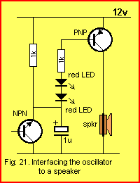
To see how this difference is arrived at, we refer to Fig: 22.
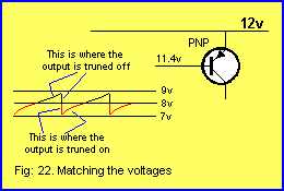
To produce a tone in the speaker, the driver transistor must be turned on and off. For this to
occur, the waveform must be higher than 11.4v at some point in the cycle.
To create this situation, we add two diodes in the form of LEDs between the output of the
oscillator and the base of the driver transistor. Each diode has a 1.7v drop, making a total of
3.4v. This voltage is effectively added to the waveform, creating an output between 10.4v and
12.4v.
It's very important to see how the LEDs are used in this situation. They have not been used as
light emitting devices but purely as a voltage drop device. We could equally use a 3.4v zener
diode (if one were available) or a series of five signal diodes. The result would be the same.
When the waveform is at 9v, the voltage difference between the output of the oscillator and the
emitter of the output transistor is 11.4 - 9 = 2.4v. This is less than the 3.4v required to
turn on the two LEDs and thus no current flows through them. This is the same if we use a
string of diodes or a zener. No current flows through this type of device until the voltage
across it (or them) reaches a potential called the zener voltage.
As the waveform drops to 8v, the voltage at the anode of the top LED is: 8 + 3.4 = 11.4v. and
the driver transistor is turned on while the waveform drops to 7v and remains on until the
waveform rises above the 8v level. The 1k base resistor separates the voltage on the LEDs from
the base voltage.
Overall, this circuit doesn't have any worthwhile applications. However it can be built for its
novelty and simplicity.
There is nothing more embarrassing than designing a project, then being told there is something
wrong with the design. This is one such incident.
It's a story about a simple circuit that, on first appearances, is difficult to find the
fault - you have to look very close.
The circuit we are talking about is shown in figure 23.
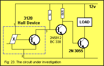
Firstly a bit of background. A Hall effect device detects the presence of magnetic flux. Some
are sensitive enough to measure the earth's magnetic flux and can be used to produce an
electronic compass. Others will detect magnetism from a bar magnet or coil etc.
Hall effect devices can range from a simple device to quite a complex item, depending on the
number of stages contained within the transistor-looking device. The number of stages determine
the sensitivity.
The device used in this circuit is fairly complex, containing an amplifier and Schmitt trigger
to give an ON-OFF output, or digital resolution, similar to a switch.
It also contains a buffer transistor capable of handling up to about 25 to 50mA. If a higher
current is required, a power amplifier can be added and this is the purpose of the two external
transistors.
The middle transistor is an inverting transistor and the third transistor is a power transistor
to drive the load.
When the Hall device detects magnetic flux, a special transistor contained inside the Schmitt
trigger symbol is turned on (a small amount). This signal is amplified by more stages then
passed to the Schmitt trigger stage that "snaps high" when the amplitude is a certain level.
This turns the linear activation of the Hall section into an ON-OFF action to drive the buffer
transistor inside the package and the output is pin 3.
The 1k resistor between pin 3 and the positive rail turns the output of the Hall device
into a digital signal and causes the output to be high (12v) when the buffer transistor is not
conducting and low (about 150mV) when the transistor is conducting.
When the Hall effect device is placed in a circuit such as figure 23, the output voltage will
not swing as high as 12v as the output is connected to the base of a transistor, we call
transistor Q2. The base prevents the output going higher than .65v and we have said the
voltage does not go lower than 0.15v when no flux is detected, so these are the two levels you
will find when you are measuring the voltages on the circuit.
Going over it again: when the Hall effect device detects a certain level of flux, the Schmitt
section causes the internal transistor on pin 3 to conduct and the voltage on pin 3 will drop
to about 150mV. This is the collector-emitter saturation voltage of the transistor.
If we now add the two external transistors, the change of state provided by the Hall effect
device will be passed to the second and third transistors and finally to the load where a
device such as relay or motor will be turned on.
Before we describe the fault with the circuit, we will explain how the second and third
transistors work.
The circuit operates in a digital mode and this means the change from one state to the other is
quick and the voltage change is a maximum.
The Schmitt symbol inside the Hall device indicates the circuit operates in this mode (fast
mode) and when no flux is detected, the buffer transistor is not conducting. This means the 1k
resistor is turning ON the second transistor and the voltage between its collector and emitter
leads is only about 150mV.
This voltage appears on the base of the output transistor and is below that required to
turn the transistor ON and thus the 2N 3055 is NOT TURNED ON.
When flux is detected by the Hall device, the buffer transistor is turned ON and the voltage
between its collector and emitter leads drops to about 150mV. This voltage appears on the base
of the second transistor and, as we know, it is not sufficient to turn the transistor on.
This is effectively the same as taking the transistor out of circuit so we have only the 2N
3055, with a 56R connected to the base.
This resistor turns the transistor ON and current passes through the collector-emitter leads
and also the load.
Now comes the fault in the design.
It revolves around the fact that any circuit should be designed to consume the least power when
it is in the non-activated state. The 56R passes about 200mA when the circuit is in the 'ON' state and the same current flows
when in the 'OFF' state.
This current is quite considerable and represents about 2.4 watts of wasted energy during the
OFF state. If you use a 56R 1/4watt resistor it would burn out! You would need a
3watt wire-wound
resistor!
If the circuit was battery operated, even a rechargeable battery would last only a day or so!
This is really wasteful and I don't know how it got past the designer of the
project or the editor of the magazine.
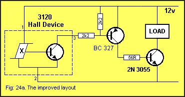
When the buffer transistor in the Hall device switches ON, current flows through the
2k2 base
resistor to turn on the second transistor. This in turn allows current to flow through the
56R
and turns ON the 2N 3055 to supply current to the load.
It's simple improvements like this that make the circuit look 'professional.'
A fault like this would not normally be picked up until the project is built and run for a few
hours, or maybe after it has been used by a customer and his battery has gone flat! Only then
would you be aware that the circuit is consuming an enormous amount of current in the
'OFF'
state.
Sometimes it is very difficult to see faults like this in a circuit diagram.
THE 56R
Why did we choose 56R for the second circuit?
The value of this resistor determines the current that can be delivered to the load and if you
want to deliver about 8 amps, here is a simple way to work out the value of the turn-on resistor.
The gain of a 2N 3055 is in the range 20 - 70, depending on the quality of the device and the
current it is handling.
We will assume the gain is 50 and allow a current flow of 8 amps.
The reason we have chosen 8 amps is due to the use of a 2N 3055 transistor. If
the current requirement was only a few amps, a low-power transistor would have
been used.
There are two instances when a very high initial current is required. When a
motor is first turned on, a very high current flows. It can be as high as
10 times the running current. The current will also be much higher than normal
when the motor is loaded. Also, when a globe is first turned on, the initial current is about 6 times the
operating current. If this current cannot be supplied, some interesting results
are produced, especially if the circuit is a flasher or flip flop. The circuit
simply does not work!
For our case, the current to be delivered to the base of the 2N 3055 is
8,000/50 =
160mA. To be on the safe side, we will deliver 200mA.
The voltage across the base resistor will be about 11v and it has to deliver 200mA, so the
value of the resistor is determined by ohms law and will be 11/.2 = 55R. We have chosen
56R.
Don't think this is an accurate determination of resistance as we are assuming the gain of the
transistor is 50 at a collector-current of 8 amps but it may be as low as 20 or 30.
What happens if the gain of the transistor is as low as 20?
The circuit will still work but the transistor will
not turn on fully and the load will not receive full-rail voltage. This is when the circuit
becomes unreliable and that's why you have to allow "a little bit up your sleeve," when
selecting component values, to allow for extreme situations and variations in manufacturing
tolerances.
Before putting this circuit to rest, you should work out the wattage consumed by the
56R
resistor.
A calculation shows the dissipation to be more than 2 watts and so the
56R should
be a 2 watt wire wound resistor.
Note that this dissipation only occurs when the globe or motor is activated.
Note: This wattage is called WASTED POWER.
If you do not want to waste energy, I suggest using a MOSFET - but this is a
subject for another discussion.
I could not end this article without including this glaring (and dangerous) mistake. LEDs are
amazing devices and are capable of emitting light when as little as 1mA is
flowing through them.
The brightness increases with current and at 25mA, the LED has reached full
brightness and its allowable heat dissipation. Even though we say a LED doesn't
get hot, it has a dissipation of 25 x 1.7 = 42 milliwatts for a 25mA current-flow.
If we pulse the LED with a slightly higher current (say 40mA) and deliver a
duty-cycle of 25% at a repetition rate of 1kHz, the LED will appear to be fully
lit and yet the actual milliwatts being delivered to it is only 40 x 1.7 x 25%
= 17mW. This is less than half the consumption for the same effective
output.
That's the advantage of strobing or pulsing a LED.
Now we come to the recent article. It stated the current through a LED could be
increased to 500 milliamps for a short period of time to get the best
efficiency out of a high-brightness LED.
We have already stated the maximum allowable current is 25mA for
continued use or 40mA in pulse-mode. Any current higher than 40mA will have the
danger of burning out the LED if something goes wrong with the circuit.
Why would you further jeopardise the situation by advancing on this feature and
saying a LED can be pulsed with 500mA of current for a very short period
of time?
You cannot improve on the efficiency by pulsing with a higher current than 40mA
for a shorter duration.
So, let's look at the circuit and see the faults:
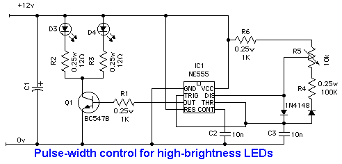
If the LED is run at 0.5 amps for very long, it will burn out (usually within
a fraction of a second). By keeping the pulse duration relatively short, we can
avoid overheating it.
The circuit above allows adjustment of the pulse width so that the maximum
average current is no more than 50mA.
To ensure long life, the circuit should be
adjusted for maximum brightness then reduced slightly to an average current of
around 40mA. One or two LEDs can be driven simultaneously. C1 can be around
1000u and acts as a reservoir because the average battery is unable to supply
half amp pulses of current. The circuit can be run from a battery or dc supply
of 9 to 12 volts.
But if someone changed the transistor for one with a higher current rating, the
LEDs would explode!
You can see the danger of presenting a circuit like this. Not only is the text
incorrect but the circuit does not behave as stated. This is simply another
circuit that has not been thoroughly tested.
Refer to the following diagram for the fault:
![]()