SPOT
THE MISTAKES!
Page 1
Page 2
Page 3
Page 4
Page 5
Page 6
Page 7
INDEX
![]()
This group of circuits comes from various books and magazines that caught the author's eye due
to one or more mistakes in a circuit diagram.
It is a positive-feedback amplifier but
you cannot instantly see this by the way it was presented in a hobby magazine.
The speaker is obviously in the collector of the output transistor and you can see how the 47n
capacitor rises when the voltage across the speaker increases.
In any case, see if you can find seven things. You may not agree with
everything I have found.
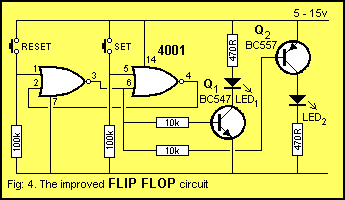
It shows the two gates used to form a bi-stable flip flop, while the other two gates are unused. Positive
logic has been used for the two switches so that their operation is easy to understand and the
resistors have been changed to the correct values. The IC has been changed to a quad NOR gate
(4001) so that positive logic can be used.
It centres around a
Three-Terminal Regulator. These are sometimes called TTR's and all regulators are adjustable to
any voltage above their minimum output voltage and up to their maximum safe working
voltage, by "jacking-up" the common terminal.
When the switch is changing from one voltage to another, the output voltage
DROPS momentarily to the lowest setting. IN the circuit above, the lowest
setting is 50% higher than the rating of the regulator. For a 5v regulator, the
lowest setting is 7v5.
It's another example of putting a circuit together without actually testing it.
The solution is to include an extra resistor called the load resistor or current limit resistor
and the value will be worked out by limiting the current to 40mA for the stair-case of LEDs and
a maximum voltage of 20v.
Don't forget the current limit resistor or you will damage the LEDs, as discussed in fig: 7.
It does not provide a HIGH above 50% of rail voltage and this is insufficient to
guarantee clocking of a digital IC. A signal above 70% of rail voltage is
needed. In 20 years, the magazine using the circuit in one of its projects did
not point out the dangers. It would be a simple matter of viewing the circuit on
a CRO to realise the output goes +50% and –20%.
The best way to learn electronics is through mistakes - either yours or others.
No-one is perfect and we all make mistakes, so it's handy to see how mistakes are made and how
they get through the proof-reading of a publication.
Some mistakes I have selected are a matter of opinion while others are definitely technical.
Maybe I'm too critical, but that's the nature of electronics.
One of the circuits discussed in this article represents a project designed by
a "fairly-competent" technical person. It is a key-hole light. He
spent months on the design and travelled overseas to complete the project and
organise manufacture of both the electronics and hardware. He then had 100,000 units manufactured and shipped to
distributors. The unit had the batteries installed because he thought the
circuit shut down to zero current. The idea was it could be operated on a display-stand so the customer could see how it worked. Unfortunately the
circuit shut down to about 60uA! By the time the units hit the shops, all the
batteries were dead! He had a total recall problem. He lost a fortune! All for
the sake of 59uA! Who said you couldn't loose a fortune over 1mA?
This is just one instance for the need for perfection - and thorough testing.
Some of the other faults that lead to the demise of "inventors" and
"suppliers" include poor quality-control where a component was missing or a wire left unsoldered.
A design has to be 100% correct for it to function. So why can't we
strive for a perfect layout and presentation of a circuit diagram?
Electronics is a universal language and even a circuit in overseas magazine can
be viewed and interpreted correctly, even though the text may be completely
indecipherable. Fortunately numerals and symbols are universal and this is just about all
you need to work out how a circuit functions.
The purpose of a circuit diagram is to make it easy to understood what the circuit
is doing. This means it must be CLEAR and include as much information as possible. All the component
values should be included as well as chip numbers and coil winding details.
If it is user-friendly it shows it was produced by a competent technical
person.
A circuit diagram is intended for you to be able to either build the device or fault-find an
existing problem.
Looking up a parts list to determine the value of a component is both time-consuming and very
frustrating. A diagram without any values does not give you any idea of how it works.
A circuit of this nature obviously has not been produced by a competent
technical person. It is
essential to know the value of each component so you can mentally work out what it is doing and
how it affects the other parts. How much more convenient to have the values
included on a diagram.
That's what POPTRONICS
Interactive Edition is all about - showing how to draw circuit diagrams
correctly and how to "see how they work."
The secret to understanding a complex circuit is to break it into simple sections called
building blocks. Many of them have (and will be) described in various articles in this e-magazine and
this way you will be able to work out how the circuit operates.
We have picked out a set of about 10 examples, here's the first:
THE OSCILLATOR CIRCUIT
The circuit to be discussed is shown in Fig: 1.
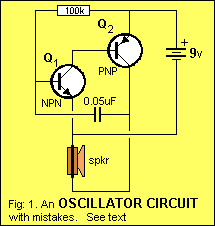
The layout doesn't follow any convention and you have to study it carefully to realise the
speaker is connected to the output transistor.
The circuit should be much clearer. It should give an instant mental picture of the operation
and you should be able to reproduce it by memory, without having to think too hard.
The second mistake is specifying non-standard values. The 0.05uF capacitor should be
marked 0.047uf or more appropriately 47n. This value comes under the group called preferred
values and our discussion on Page 18 of the Basic
Electronics Course explains the range of preferred values
for capacitors and also lists design values, such as 10n, 22n, 47n, and 100n.
These are used in designs if the value is not important. They convey to the reader that the
value is a non-critical.
The third mistake is the battery symbol. It shows two cells in series, or 3v. A 9v battery is
multi-cell and the correct symbol is shown in fig: 2.
But the most dangerous fault is the connection of the two transistors directly across the
supply.
If you follow the circuit you will find a current path through two junctions with no
current-limiting resistor.
From the positive rail, the current can flow through the base-emitter of the PNP transistor and
the collector-emitter of the NPN transistor without limit.
When the circuit is first turned on, the 100k resistor begins to turn on the NPN transistor and
this starts to turn on the PNP transistor. Current flows through the speaker. This puts a
voltage-drop across it and creates a click. The right hand side of the 0.05u capacitor rises
and takes the left side up too.
The capacitor is slightly charged and all this charge goes into the base of the NPN transistor.
This turns it on almost fully. A large current flows through the collector-emitter junction
of the NPN transistor and this current comes via the base-emitter junction of the PNP
transistor. This current will be higher than the allowable amount and may damage the
transistor.
The high current will also cause the supply voltage to fall and reduce the voltage to the
speaker, so the speaker will not be as loud as in fig: 2. The corrected circuit is shown
below. It is much easier to see exactly what is happening.
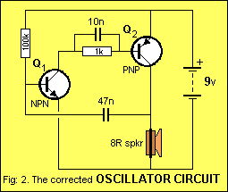
The 1k between the two transistors acts as a current limiter to prevent the two transistors
being damaged.
The 10n allows a high pulse of current to flow in the base-emitter circuit of the PNP
transistor, without damaging it and fully turns it on to drive the speaker.
The second circuit will take less current to achieve exactly the same result as in fig: 1, and
avoid high currents flowing through the junctions of the transistors.
The second circuit clearly shows the two transistors are a directly coupled high gain amplifier
with the speaker as the collector load of the output transistor.
The circuit works on regenerative action (positive feedback).
This is where one section passes a signal to another and it is amplified and returned to the
first to make the signal even larger. This happens until the signal is as high as possible
(generally almost as large as the supply voltage) and since it cannot get any larger, something
happens to reverse the situation, so the signal gets as small as possible and the cycle
repeats.
In our case the cycle starts with the 100k on the base of the first transistor charging the
47n capacitor and when the voltage is above 0.65v, the transistor begins to tun on.
This turns on the second transistor and a current flows through the collector-emitter junction
and also the speaker.
When a current flows through a load such as a speaker, a voltage is developed across it and
this voltage is seen by the right side of the 47n capacitor. The right side of the capacitor
rises and takes the left side up with it.
The charge on the capacitor is dumped into the base of the first transistor and this makes it
turn on even harder.
This action continues around the circuit until both transistors are fully turned on. This is
called positive feedback.
They stay fully tuned on for a short period of time and then the capacitor runs out of charge.
This makes the NPN transistor turn off slightly. This turns off the PNP transistor and the
voltage across the speaker reduces and the capacitor drops slightly. This puts less voltage on
the base of the NPN transistor and it turns off. This action continues around the circuit until
both transistors are fully turned off.
The 100k resistor begins to charge the 47n to start the cycle again.
This action repeats 500 to 5,000 times per second, depending on the value of the
capacitor (47n) and 100k resistor. If the capacitor is reduced in value, the frequency is
increased. If the resistor is increased in value, the frequency is reduced.
THE FLIP FLOP CIRCUIT
The second circuit we will discuss is shown in fig: 3. It was found in a project booklet for
beginners and contains no fewer than seven mistakes. Some you will agree with while others will
create a debate.
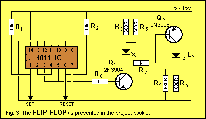
1. The first, and most obvious mistake is the 1k resistors on the base of the transistors. A 1k
resistor is a very low value for a small-signal transistor. It will deliver about 15mA to the
base and this is too high. The base should see no more than 1mA. In this case the resistor
should be 10k to 47k.
2. The 4011 IC is a CMOS device and has high impedance inputs. It should have 100k to 1M for the
pull-up resistors.
3. The supply voltage of 15v is getting very close to the maximum voltage for some CMOS chips.
Some have a maximum of 15v or 18v, or 22v, depending on the manufacturer.
CMOS should be limited to 12v to be on the safe side.
4. The circuit has two 680R resistors in parallel as the load resistors for the Light Emitting
Diodes. The supply voltage is in the range 5 - 15v.
With a 15v supply, the current through the LEDs will be nearly 36mA and this is higher
than the allowable maximum. LEDs are rated at 20mA for normal operation. The current can be
increased to 25-30mA for short periods and up to 40mA in pulse mode.
5. When designing a circuit such as this, it is normal for a switch to give a positive pulse
when it is closed. This is called positive logic and is the easiest logic to
understand.
The opposite logic is called negative logic in which a negative pulse (or zero pulse) is
applied to an input when a switch is closed. The SET and RESET switches in fig: 3 introduce negative logic
and this makes the circuit difficult to understand. (In fig: 4 we have given the switches positive logic.)
6. The LEDs are identified as L1 and L2. The letter 'L' is reserved for coils
and inductors not LEDs. LEDs are diodes and are given the letters LED1
, LED2 etc.
The two additional 680R resistors have the same part number
R5. They should be R5 and R8. Every component must have its own separate part number. This mistake was carried
through to the parts list where it specified 3 x 680R!
7. Now here is the most interesting fault.
The circuit description says both LEDs will come on when pin 3 is HIGH and go off when pin 3 is
LOW. But what is the point of having the second transistor to drive the second LED? Both LEDs
could be placed in series with each other and this would save 3 or 4 components.
A better arrangement is to have the circuit drive two LEDs independently as shown in fig: 4. For
this, the two base resistors of the transistors go to pin 3 of the IC.
The diagram in figure 3 is not really a circuit diagram or schematic. The wiring around the
chip may be suitable for the beginner so he can wire up the chip but the block diagram
for the chip does not
tell you anything about the type of gates inside the chip. You would have to refer to a
technical manual to find out the 4011 is a quad NAND gate.
The purpose of a circuit diagram or schematic is to show all the symbols so the reader can
instantly work out what is happening.
The layout in figure 3 doesn't help you understand how the circuit works and this form of
presentation is to be avoided.
The preferred way of laying out the circuit is shown in fig: 4.
AN ADJUSTABLE REGULATOR
The third faulty circuit is shown in fig: 5.
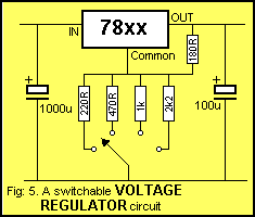
For a 5v regulator the output can be between 5v and 35v. For a 12v regulator it
can be 12v to 40v and for a
LM 317, it can be 1.2v to 37v. There are other factors that come in to the ability of a regulator
to deliver the current at a particular voltage and this is mainly the result of wattage
dissipated in the package. This will be covered in other articles.
The Common terminal is sometimes called the adj (adjust) pin and any increase on this pin is passed
to the output via the circuitry inside the package.
The electronics inside the package is not simply one or two transistors and a few
resistors. It
is a complex monitoring circuit requiring 20 or more transistors to maintain a constant output
voltage over a wide range of current fluctuations. It also has thermal detection to prevent the
package getting too hot and current limiting to prevent overload.
Three terminal regulators are very inexpensive for the operation they perform.
Now back to the problem. The fault with fig: 5 is mainly mechanical.
The rotary switch used to change from one voltage to another is a break-before-make type and
this means there will be a very short period of time when no voltage divider resistor is
connected to the ground or earth rail.
This means the 180R "pull-up" resistor will pass the full output voltage to the common pin and
increase the common terminal by a value equal to the voltage of the regulator. If the regulator
is a 7805, the output voltage will increase by 5v to 10v. The 10v will be passed back to the
common pin and the output will rise a further 5v. The output will keep rising until it is about 4v less than the input and this could be 25v or
higher!
Any voltage-sensitive equipment being supplied by the regulator will get a pulse of very high
voltage during switching and may be damaged.
The correct way to add a selector switch to a regulator is shown in fig: 6.
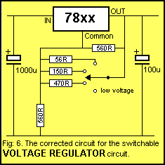
The "low voltage" setting of the switch does not need any connections
as it represents 7v5.
As the other positions are selected, the output voltage is jacked up and when the switch is
between positions, the voltage drops to the "lowest value."
The resistance values given in the diagram are only examples and you will have to work out
values for your particular voltages.
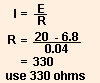
5-LED VOLTAGE INDICATOR
The next circuit, shown in fig:7, is a very simple voltage indicator using 5 LEDs to indicate voltages from
about 5.5v to 8.5v.
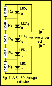
This is one of the things we don't do. We never present a circuit without actually trying it
first because things always creep in where you least expect them. This circuit is a typical
example.
The author obviously didn't try the circuit because if he had, it would have blown up!
The text says "The two test points are applied to the unknown voltage with the polarity shown."
Can you see what would happen to the circuit if the unknown voltage is 12v?
If not, we will go into a little theory about LEDs, but first let's look at the voltage at
which each LED will start to illuminate.
The circuit is perfect in theory - just one resistor has been left off. The parts list did not
specify the colour of the LEDs and this is important as each colour has a different
characteristic voltage that develops across it and once this voltage is reached, it does not
increase.
The other fault is the specification of "oddball" resistors. It doesn't really matter what
voltage each LED turns on at, provided the resistors are easy to obtain.
The corrected diagram is shown below but don't refer to it until you have tried to
work out what is wrong with the original circuit.
Here's how to work out the turn-on voltage for each LED.
Firstly we will specify red LEDs for the ladder and a red LED turns on when the voltage across
it is 1.7v. Some red LEDs need 1.8v - 1.9v so your ladder will need to be calibrated before
use.
Let us use 1.7v red LEDs. Suppose we start with a voltage that increases from zero. When the
voltage is low, the LEDs exhibit infinite resistance and do not put any load on the circuit.
The only components in the circuit are the chain of resistors.
A voltage will develop across each resistor according to its value and as the voltage rises,
the 550 ohm resistor will create the highest voltage across it. This means the 550 ohm resistor
is the first resistor we look at.
When the voltage across it is 1.7v, each of the other resistors will have a voltage across them
according to its resistance. Resistor R2 will have 1.23v, R3
will have 0.93v, R4 will have 0.62v, R5 will have 0.3v, making a total of
4.8v.
You can see the only resistor with enough voltage across it to turn on a LED is R1 and
this occurs when the test voltage is 4.8v.
Here comes the next surprise. The voltage across LED1 does not rise any higher
than 1.7v. As more current flows though the circuit, the LED gets brighter but the voltage across it
does not increase.
This feature has to be taken into account when working out the rest of the calculations.
As the voltage increases, the voltage across R2 becomes 1.7v, and LED2 begins to
turn on. When the voltage across R2 is 1.7v, the voltage across the total of R3,
R4 and R5 is 1.27 + 0.85 + 0.42 = 2.54v
This makes the test voltage = 1.7v + 1.7v + 2.54v = 5.94v.
We really don't have to get into accuracy like this but it has been presented to show you how
to work out the various values.
LED3 turns on at 6.79v. LED3 turns on at 7.65v and LED5 turns on at 8.5v.
Remember what we said about the characteristic voltage of LED. The voltage does not rise above
1.7v.
If you supply the circuit with a voltage above 8.5v, the LEDs are not going to allow the
voltage to rise above 8.5v and any voltage above this is simply going to drive more current
through them. When the current rises above 40mA, one or more will be permanently damaged.
This has not been taken into account when the circuit was designed and is a bad omission.
The answer is the circuit shown in fig: 8:
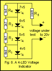
By Ohms law:
Now we have to work out a set of resistances for the ladder so the LEDs come on at about the
same voltages as before.
The 330R current limiting resistor sets the parameters for this circuit and has turned it into
a very complex design problem.
The whole circuit will have to be designed around very low current because the 330R resistor
has set the minimum current.
It works like this:
Firstly we will not be able to have 5 LEDs. Only 4 will operate with the new design.
Secondly we have to assume a LED starts to illuminate when 0.5mA is flowing through it. If you
test a LED you will be able to see a faint glow when this current is flowing.
If the LEDs are exactly 1.7v devices, the top LED will turn on at 7v5 and at 9v, it will have
about 6mA flowing through it.
For LED3 to turn on at 6.5v, resistor R4 must be 1k5.
Working out the values for the staircase of resistors is a lot of work and beyond the scope of
this article.
A LED is very similar to a zener diode. In fact it is exactly like a zener diode with a window
so you can see the current flowing.
A red LED is a 1.7v zener diode. A green LED is about 2.1v zener and orange is about 2.3v.
As soon as the voltage reaches 1.7v or 2.1v or 2.3v, the voltage across the device does not
increase. All that happens is the current through the LED increases when you try to put a
higher voltage across it.
The increased current flow can be seen by the increase in the brightness of the LED.
In fact you can use a LED as a zener diode and see how a normal zener operates.
You can create any zener voltage by putting LEDs in series as shown in fig: 9.
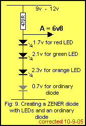
The zener voltage appears between point "A" and the 0v rail. In the example of fig: 9, the
voltage will be 1.7 + 2.1 + 2.3 + 0.7 = 6.8v.
Almost any voltage from 0.7v can be created, depending on the combination of LEDs and ordinary
signal diodes.
THE TOUCH SWITCH
The following Touch Switch circuit misses the point of the high impedance
front-end. The 1M on the base of the BC557 is a very high value and will
give the transistor very little current capability to make the output of the
circuit HIGH.
The super-alpha pair on the front end (made up of the two BC547 transistors)
has already created a low impedance output (as shown by the 10k on the
output), so the line can be driven low when a finger is placed on the Touch
Plates. The 1M could be lowered to 47k to give the output more "driving
power" and show that the front-end has produced a low impedance arrangement. 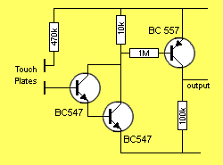
THE OSCILLATOR
Here's an oscillator circuit that
doesn't work: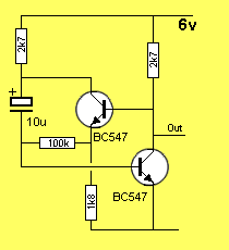
Maybe that's why this circuit has never been repeated in any other magazine.