;*******************************
;;8x8 Module.asm
;
; 23-6-2013
;*******************************
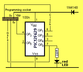
list p=12F629
radix dec
include "p12f629.inc"
errorlevel -302 ; Don't complain about
;BANK 1 Registers during assembly
__CONFIG _MCLRE_OFF & _CP_OFF & _WDT_OFF & _INTRC_OSC_NOCLKOUT
;_MCLRE_OFF - master clear must be off for gp3 to work as input pin
;****************************************************************
; variables - names and files
;****************************************************************
Cblock 20h
temp1 ;used in delays
temp2 ;used in delays
temp3 ;used in EEPROM data fetching
temp4 ;used in EEPROM data fetching
temp5 ;used in EEPROM data fetching
temp6 ;used in EEPROM data fetching
current ;holds current EEPROM location
letters ;letters holds the number of letters in EEPROM
serial
address
_data
jump ;table1 jump value
columns ;for 6 columns
Sw_Flag ;detecting sw-press
eefile ;total number of characters in EEPROM
endc
;****************************************************************
;Equates
;****************************************************************
status equ 0x03
rp1 equ 0x06
rp0 equ 0x05
GPIO equ 0x05
status equ 03h
option_reg equ 81h
; bits on GPIO
pin7 equ 0 ;GP0 LED - flashes to indicate key number
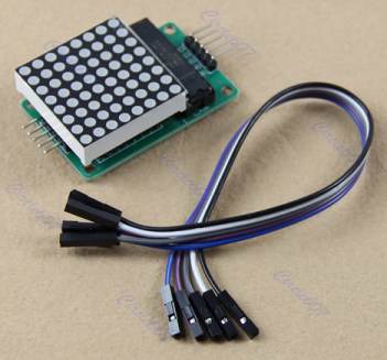
pin6 equ 1 ;GP1 Data to 8x8 Module
pin5 equ 2 ;GP2 Chip Select
pin4 equ 3 ;GP3
pin3 equ 4 ;GP4 Clock
pin2 equ 5 ;GP5 4 switches
;bits
rp0 equ 5 ;bit 5 of the status register
;****************************************************************
;Beginning of program
;****************************************************************
org 0x00
goto SetUp
;****************************************************************
;Table
;****************************************************************
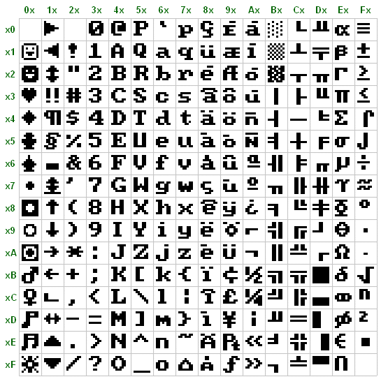
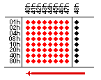
table1 addwf 02h,1 ;add W to program counter
dt 7Eh,09h,09h,09h,7Eh,00h ;A
dt 7Fh,49h,49h,49h,36h,00h ;B
dt 3Eh,41h,41h,41h,22h,00h ;C
dt 7Fh,41h,41h,22h,1Ch,00h ;D
dt 7Fh,49h,49h,41h,00h,00h ;E
dt 7Fh,09h,09h,01h,00h,00h ;F
dt 3Eh,41h,49h,49h,3Ah,00h ;G
dt 7Fh,08h,08h,08h,7Fh,00h ;H
dt 7Fh,00h,00h,00h,00h,00h ;I
dt 20h,40h,40h,3Fh,00h,00h ;J
dt 7Fh,08h,14h,22h,41h,00h ;K
dt 7Fh,40h,40h,40h,00h,00h ;L
dt 7Fh,06h,18h,18h,06h,7Fh ;M
dt 7Fh,02h,0Ch,18h,20h,7Fh ;N
dt 3Eh,41h,41h,41h,3Eh,00h ;O
dt 7Fh,09h,09h,09h,06h,00h ;P
dt 1Eh,21h,31h,21h,5Eh,00h ;Q
dt 7Fh,09h,19h,29h,46h,00h ;R
dt 26h,49h,49h,49h,32h,00h ;S
dt 01h,01h,7Fh,01h,01h,00h ;T
dt 3Fh,40h,40h,40h,3Fh,00h ;U
dt 0Fh,30h,40h,30h,0Fh,00h ;V
dt 3Fh,40h,38h,40h,3Fh,00h ;W
dt 63h,14h,08h,14h,63h,00h ;X
dt 03h,0Ch,70h,0Ch,03h,00h ;Y
dt 61h,51h,49h,45h,43h,00h ;Z
dt 42h,7Fh,40h,00h,00h,00h ;1
dt 72h,49h,49h,49h,46h,00h ;2
dt 22h,41h,49h,49h,36h,00h ;3
dt 18h,14h,12h,7Fh,10h,00h ;4
dt 2Fh,49h,49h,49h,31h,00h ;5
dt 3Eh,49h,49h,49h,32h,00h ;6
dt 01h,71h,09h,05h,03h,00h ;7
dt 36h,49h,49h,49h,36h,00h ;8
dt 26h,49h,49h,49h,3Eh,00h ;9
dt 00h,00h,00h,00h,00h,00h ;space (0D8h)
;****************************************************************
;Set Up
;****************************************************************
SetUp bsf status, rp0 ;Bank 1
movlw b'11001000' ;Set TRIS GP0,1,2,4,5 out GP3 not used
movwf TRISIO
bcf status, rp0 ;bank 0
movlw 07h ;turn off Comparator ports
movwf CMCON ;must be placed in bank 0
clrf GPIO ;Clear GPIO of junk
clrf jump
clrf 40h ;clear files for RUN
clrf 41h
clrf 42h
clrf 43h
clrf 44h
clrf 45h
clrf 46h
clrf 47h
;Delete EEPROM Data - pressing "RUN" before switch-ON
;deletes DATA by zeroing the number of letters in address 07h
call SwPressed
btfss Sw_Flag,4 ;see if "Run" switch pressed
goto Main ;not pressed
movlw 7Fh
bsf status,rp0 ;select bank1
movwf eeadr
bcf status,rp0 ;select bank0
clrw
bsf status,rp0 ;select bank1
movwf eedata
bcf status,rp0 ;select bank0
call write
call SwPressed
btfsc Sw_Flag,4 ;see if "Run" switch not pressed
goto $-2
goto Main
;****************************************************************
;* Delays *
;****************************************************************
_6uS goto $+1
retlw 00
_12uS goto $+1
goto $+1
goto $+1
goto $+1
retlw 00
_1mS nop
decfsz temp1,f
goto $-2
retlw 00
_10mS movlw .10
movwf temp2
call _1mS
decfsz temp2,f
goto $-2
retlw 00
_50mS movlw .50
movwf temp2
_50 nop
decfsz temp1,f
goto _50
decfsz temp2,f
goto _50
retlw 00
_100mS movlw .100
movwf temp2
_100 nop
decfsz temp1,f
goto _100
decfsz temp2,f
goto _100
retlw 00
;****************************************************************
;* Sub Routines *
;****************************************************************
Dec_Jump
decf jump,f
decf jump,f
decf jump,f
decf jump,f
decf jump,f
decf jump,f
retlw 00
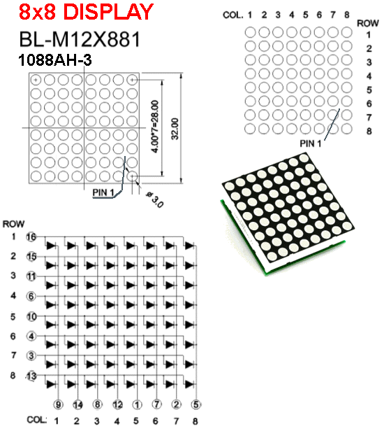
;creates blank column 1,data for cols:234567 and blank col8
Display
movlw 0D8h ;Look for end of table
xorwf Jump,w
btfss status,z ;zero bit will be set if the same
goto $+2
clrf jump ;start at top of table
clrf address
incf address,1 ;col1 = address 1
clrf _data
call Load
movlw 6
movwf columns ;load counter for 6 columns
incf address,1
movf Jump,w ;move jump value into w
call table1 ;get jump value for table1
movwf _data ;load data from table1 into _data
call Load
incf jump,1 ;increment jump value for table1
decfsz columns,f
goto $-7
incf address,1 ;col8 = address 8
clrf _data
call Load
retlw 00
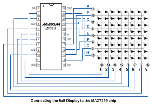
;send 16 bits to 8x8 Module
;address 0 - 7 for columns
;and data for each column
Load bcf gpio,2 ;open chip to receive address and data
movlw 8
movwf serial ;load loop counter with 8 to transfer 8 bits
movf address,w
movwf temp3
rlf temp3,f ;move bit through carry
rlf temp3,f ;move bit to bit0 position
btfss temp3,0 ;these 3 instructions are very clever!!!!
bcf gpio,1 ;to send LOW data bit
btfsc temp3,0 ;see if the lowest bit is 0 or 1
bsf gpio,1 ;to send HIGH data bit
rlf temp3,f ;put here to separate two gpio commands
bsf gpio,4 ;clock HIGH
call _12uS ;must have small delay between bsf and bcf
bcf gpio,4 ;clock LOW to lock-in data bit
decfsz serial,f
goto $-9
;send 8 bits DATA
movlw 8
movwf serial ;load loop counter with 8 to transfer 8 bits
rlf _data,f ;move bit 7 to bit 0 position
rlf _data,f
btfss _data,0
bcf gpio,1 ;to send LOW data bit
btfsc _data,0 ;see if the lowest bit is 0 or 1
bsf gpio,1 ;to send HIGH data bit
rlf _data,f ;put here to separate two gpio commands
bsf gpio,4 ;clock HIGH
call _12uS
bcf gpio,4 ;clock LOW to lock-in data bit
decfsz serial,f
goto $-9
bsf gpio,2 ;close chip
retlw 00
;create non-shutdown mode
noshutdown
bcf gpio,2 ;open chip to receive address and data
movlw 8
movwf serial ;load loop counter with 8 to transfer 8 bits
movlw 0Ch ;0Ch accesses shutdown register
movwf address
rlf address,f ;move bit 7 to bit 0 position
rlf address,f
btfss address,0 ;these 3 instructions are very clever!!!!
bcf gpio,1 ;to send LOW data bit
btfsc address,0 ;see if the lowest bit is 0 or 1
bsf gpio,1 ;to send HIGH data bit
rlf address,f ;put here to separate two gpio commands
bsf gpio,4 ;clock HIGH
call _12uS
bcf gpio,4 ;clock LOW to lock-in data bit
decfsz serial,f
goto $-9
movlw 8
movwf serial ;load loop counter with 8 to transfer 8 bits
movlw 7 ;1 needed in data register for normal operation
movwf _data ;
rlf _data,f ;move bit 7 to bit 0 position
rlf _data,f
btfss _data,0
bcf gpio,1 ;to send LOW data bit
btfsc _data,0 ;see if the lowest bit is 0 or 1
bsf gpio,1 ;to send HIGH data bit
rlf _data,f ;put here to separate two gpio commands
bsf gpio,4 ;clock HIGH
call _12uS
bcf gpio,4 ;clock LOW to lock-in data bit
decfsz serial,f
goto $-9
bsf gpio,2 ;close chip
retlw 00
;Run - scrolls message across screen data held in 40h to 4Fh
Run movlw 7Fh ;get number of letters from EEPROM 7Fh
bsf status,rp0 ; select bank 1
movwf eeadr ; look at 7Fh
bsf eecon1,rd ; initiate the read
movf eedata,w ; put the read data into w
bcf status,rp0 ;
movwf letters ;letters holds the number of letters
RunAA clrf current ;holds current EEPROM location
RunA movf current,w ;first location in EEPROM
bsf status,rp0 ; select bank 1
movwf eeadr ; look at 00h
bsf eecon1,rd ; initiate the read
movf eedata,w ; put the read data into w
bcf status,rp0 ;
movwf temp5 ;temp5 holds table jump value
movf current,w ;end of message?
xorwf letters,w
btfsc status,z ;zero bit will be set if the same
goto RunAA ;go to start of message
movlw 6
movwf temp6 ;6 columns for each letter
RunB movf temp5,w ;put jump-value into w
call table1
movwf 48h ;put column-value into ghost column
call Shift ;create "running effect"
movlw 40h
movwf 4 ;fsr for indirect addressing
clrf address ;col1 = address 1
movlw 8
movwf columns ;load counter for 8 columns
incf address,f ;for column 1
movf 0,w ;move data from file 40h into w
movwf _data ;move data to _data file
call Load
incf 4,f ;increment FSR to look at file 41h
decfsz columns,f
goto $-6
call noshutdown ;tell8x8 to illuminate display
call Scancols ;tell 8x8 to scan 8 columns
call _100mS
call _100mS
incf temp5,f ;jump value for each letter
decfsz temp6,f ;loop counter for 6 columns
goto RunB
incf current,f
goto RunA
;scan all columns
Scancols
bcf gpio,2 ;open chip to receive address and data
movlw 8
movwf serial ;load loop counter with 8 to transfer 8 bits
movlw 0Bh ;0Bh accesses scan-limit register
movwf temp4
rlf temp4,f ;move bit 7 to bit 0 position
rlf temp4,f
btfss temp4,0 ;these 3 instructions are very clever!!!!
bcf gpio,1 ;to send LOW data bit
btfsc temp4,0 ;see if the lowest bit is 0 or 1
bsf gpio,1 ;to send HIGH data bit
rlf temp4,f ;put here to separate two gpio commands
bsf gpio,4 ;clock HIGH
call _12uS
bcf gpio,4 ;clock LOW to lock-in data bit
decfsz serial,f
goto $-9
movlw 8
movwf serial ;load loop counter with 8 to transfer 8 bits
movlw 7 ;7 is needed to scan 8 columns
movwf temp4
rlf temp4,1 ;move bit 7 to bit 0 position
rlf temp4,1
btfss temp4,0
bcf gpio,1 ;to send LOW data bit
btfsc temp4,0 ;see if the lowest bit is 0 or 1
bsf gpio,1 ;to send HIGH data bit
rlf temp4,f ;put here to separate two gpio commands
bsf gpio,4 ;clock HIGH
call _12uS
bcf gpio,4 ;clock LOW to lock-in data bit
decfsz serial,f
goto $-9
bsf gpio,2 ;close chip
retlw 00
;shift columns to the LEFT also removes blank columns
Shift movf 41h,w ;shift columns to the left
movwf 40h
movf 42h,w
movwf 41h
movf 43h,w
movwf 42h
movf 44h,w
movwf 43h
movf 45h,w
movwf 44h
movf 46h,w
movwf 45h
movf 47h,w
movwf 46h
movf 48h,w
movwf 47h
retlw 00
;SwPressed sets bit 4, 3, 2, 1 in switch-flag
SwPressed
clrf Sw_Flag ;clear the switch flag
bsf status, rp0 ;Bank 1 (see if switch is pressed)
bcf TRISIO,5 ;clear bit GPIO,5 as output to charge cap.
bcf status, rp0 ;bank 0
bsf gpio,5 ;make pin2 HIGH to charge cap.
call _10mS ;charge cap
bsf status, rp0 ;Bank 1
bsf TRISIO,5 ;set TRIS GP0,5 to detect discharged cap
call _1mS ;create a delay to see if no sw pressed
btfss gpio,5
goto $+3
bsf Sw_Flag,7 ;no switch pressed
retlw 00
bsf status, rp0 ;Bank 1
bcf TRISIO,5 ;clear bit GPIO,5 as output to charge cap.
bcf status, rp0 ;bank 0
bsf gpio,5 ;make pin2 HIGH to charge cap.
call _10mS ;charge cap
bsf status, rp0 ;Bank 1
bsf TRISIO,5 ;set TRIS GP0,5 to detect discharged cap
bcf status, rp0 ;bank 0
call _12uS
call _12uS
call _12uS
call _6uS
btfsc gpio,5
goto $+3
bsf Sw_Flag,4
retlw 00
call _12uS
btfsc gpio,5
goto $+3
bsf Sw_Flag,3
retlw 00
call _12uS
call _6uS
btfsc gpio,5
goto $+3
bsf Sw_Flag,2
retlw 00
call _12uS
btfss gpio,5
bsf Sw_Flag,1
retlw 00
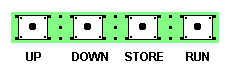
;Sw3 = STORE - stores address of character (table1) into EEPROM
;eefile - total number of characters in EEPROM 217Fh
;eedata will be jump value
;eeadr will be zero at start-up
Store
;look at 7Fh in EEPROM
movlw 7Fh ;get location in EEPROM for storing next value
bsf status,rp0 ; select bank 1
movwf eeadr ; look at 7Fh
bsf eecon1,rd ; initiate the read
movf eedata,w ; put the read data into w
bcf status,rp0 ;
movwf eefile ;and move to eefile
movf eefile,w ;starts at 0 for EEPROM 1st location
bsf status,rp0 ;select bank1
movwf eeadr
bcf status,rp0 ;select bank0
call Dec_Jump
movf jump,w ;dec jump 6 times to get start of letter
bsf status,rp0 ;select bank1
movwf eedata
bcf status,rp0 ;select bank0
call write
incf eefile,f ;increment to store in next EEPROM location
movlw 7Fh ;store in EEPROM last location
bsf status,rp0 ;select bank1
movwf eeadr
bcf status,rp0 ;select bank0
movf eefile,w ;store the number of letters
bsf status,rp0 ;select bank1
movwf eedata
bcf status,rp0 ;select bank0
call write
retlw 00
write bsf status,rp0 ;select bank1
bsf eecon1,wren ;enable write
movlw 55h ;unlock codes
movwf eecon2
movlw 0aah
movwf eecon2
bsf eecon1,wr ;write begins
bcf status,rp0 ;select bank0
writeA btfss pir1,eeif ;wait for write to complete
goto writeA
bcf pir1,eeif
bsf status,rp0 ;select bank1
bcf eecon1,wren ;disable other writes
bcf status,rp0 ;select bank0
retlw 00
;****************************************************************
;* Main *
;****************************************************************
Main
clrf Sw_Flag ;clear the switch flag
call Display ;creates blank col1,
;data for cols:234567 and blank col8
call noshutdown
call Scancols
clrf Sw_Flag ;go to here for looping
call SwPressed
btfss Sw_Flag,7 ;see if no switch pressed
goto $+2 ;sw pressed
goto $-4 ;no sw pressed
btfss Sw_Flag,1 ;see if "Forward" switch pressed
goto $+7 ;see if other switch pressed
Main1 call Display
clrf Sw_Flag
call SwPressed
btfss Sw_Flag,7 ;see if no switch pressed
goto $-3
goto $-.12
btfss Sw_Flag,2 ;see if "Back" switch pressed
goto $+9
call Dec_Jump
call Dec_Jump
movlw 0FAh
xorwf Jump,w
btfss status,z ;zero bit will be set if the same
goto $+3
movlw 0D2h ;address of last letter
movwf jump ;go to bottom of table
btfss Sw_Flag,3 ;see if "Store" switch pressed
goto $+2
call Store
btfss Sw_Flag,4 ;see if "Run" switch pressed
goto Main1
call Run
;****************************************************************
;*EEPROM Values to burn into EEPROM *
;****************************************************************
org 2100h ;org 2100h means the next byte of data will
;>be at location 00 in EEPROM
de 00h ;de means Data EEPROM
org 217Fh
de 00h ;newly burnt chip:
;00 for number of char in EEPROM
END
|