|
BASIC
ELECTRONICS COURSE
TOUCH
SWITCH
A simple circuit to show the
operation of a NAND gate.
Note: No kit is available for this circuit.
Page 27  INDEX
INDEX
Before reading the
article, go to the two animations below and see how the circuit operates.
HOW THE CIRCUIT
WORKS
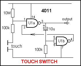
The chip used in this project is a Quad 2-input NAND gate. It normally goes
under the part-number
CD 4001 or HCF 4001 or simply "the 4000 family."
Only two of the gates are used. Read page
26 of this course to
see how a NAND gate operates.
The second gate in the circuit has both inputs tied together and this changes
it from a NAND operation to an inverter (NOT gate). So, there is
only one NAND gate and one INVERTER in the circuit.
When power is applied, pin 1 of the first NAND gate will be pulled HIGH by the
action of the 10M resistor. The output of the gate will be worked out in a
minute, we now go to the input of the second gate and see it has a
TIME DELAY CIRCUIT connected to it. A capacitor and resistor connected in series
is called a "Time Delay" circuit. It does not matter if we consider
the output of U1a is HIGH or low. With any time-delay circuit, the capacitor
will be charged after a period of time and so the voltage on the input of the
INVERTER will be LOW.
This makes the output HIGH and the high is transferred back (called a
FEEDBACK LINE) to the first gate. Thus U1a has a HIGH on both inputs and the
output is LOW.
This is how the circuit "SITS" with the output LOW.
If a finger is briefly placed across the two touch pads, the voltage on
pin 1 will go LOW.
The output of U1a goes HIGH and since the capacitor is uncharged, it takes the
input of the inverter HIGH. The output of the inverter goes LOW and this is
passed to input pin 2 of U1a. In effect, the action of the circuit is taking
the place of your finger as far as U1a is concerned and you can now remove it
from the Touch Pads.
The 10u electrolytic starts to charge and after a short period of time the
voltage on the input of U1b goes LOW. This makes the output of U1b HIGH
and this is transferred to pin 2 of the first gate.
If your finger has been removed before this "time-out," U1a will see
two HIGHs (a HIGH on each of the two input pins) and the output will go LOW. The fully charged capacitor will be
discharged through a diode on the input line of the second gate, and the circuit
will sit in this state until it is activated again.
A LITTLE KNOWN
FACT
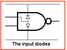 A set of diodes is present on each
input line to prevent the input voltage rising above or falling below the rail
voltages.
A set of diodes is present on each
input line to prevent the input voltage rising above or falling below the rail
voltages.
Under normal conditions these diodes are "reverse biased" and do not
have any effect on the operation of the gate.
But if the input voltage rises above rail voltage, the top diode becomes
forward biased and "clips" the input voltage to rail voltage + 0.65v
above rail voltage. The same applies to the negative excursion. The input
voltage is clipped to -.65v
This is how the electrolytic gets discharged. It discharged through the
lower diode. When the output of the first gate goes low, the charged
electrolytic will try to take the input(s) of the second gate to about -9v (if
the rail voltage is 10v). But the lower diode on the input prevents it going
more than -.65v and thus the electrolytic is discharged through it.
See the action of the capacitor by referring to the multivibrator animations on
the previous pages of this course.
CIRCUIT
OPERATION
When a finger is placed on the "Touch Pads" (and removed very
quickly) the output of the circuit goes HIGH, remains HIGH for a short period
of time, then goes LOW. In other words the circuit produces a brief pulse when
a finger touches the Touch Pads.
There are two animations for this circuit:
A: The first animation shows the operation of the circuit if a finger is
kept on the touch pads for a long period of time. The circuit
"times-out" but does not change state. This is not how the
circuit is intended to be used. It only requires a brief touch of the pads for
the circuit to operate correctly. Keep the mouse on the Touch Pads to see
how the circuit reacts.
B: The second animation shows the correct operation of the circuit. Move the
mouse quickly over the Touch Pads to see it operate.
In the first animation, the things to observe are:
1. Pin 1 goes LOW when a finger is placed on the Touch Pads.
2. Output of U1a goes HIGH.
3. Electrolytic is uncharged and takes input of U1b HIGH.
4. Output of U1b goes LOW.
5. Pin 2 of U1a goes LOW.
6. Electrolytic begins to charge.
7. After a period of time, input of U1b sees a LOW from the "timing
circuit"
8. Output of U1b goes HIGH
9. Pin 2 goes goes HIGH but NAND gate does not change because a finger is on
the Touch Pad is keeping pin 1 LOW.
In the second animation, the things to observe are:
1. Pin 1 goes LOW when a finger is placed on the Touch Pads.
2. Output of U1a goes HIGH.
3. Electrolytic is uncharged and takes input of U1b HIGH.
4. Output of U1b goes LOW.
5. Pin 2 of U1a goes LOW.
6. Pin 1 goes HIGH when finger is removed..
7. Electrolytic begins to charge.
8. After a period of time, input of U1b sees a LOW from the "timing
circuit"
9. Output of U1b goes HIGH
10. Pin 2 goes goes HIGH.
11. Output of NAND gate goes LOW.
THE
"TIME DELAY" CIRCUIT
The capacitor and resistor make up a circuit known as a TIME DELAY CIRCUIT.
When power is applied to the combination, the capacitor charges via the
resistor and the voltage at the join can be monitored. The capacitor can be
placed above or below the resistor and the voltage at the join will
either rise or fall during the charging process. It does not matter if the
voltage rises or falls, the end result is the same.
We are waiting for a CHANGE from LOW to HIGH or HIGH to LOW and the time
for this to occur is the feature of the circuit.
The join of the time delay components (the point on the circuit where the
capacitor and resistor meet) is monitored by one of the input lines of the NAND
gate and in the Touch Switch circuit, the capacitor
is above the resistor. This means the voltage will fall when the capacitor
begins to charge. A point is reached where the gate sees a LOW and the output
goes HIGH.
Keep your mouse on the Touch Pads to see the operation
of the circuit if a
finger is kept on the pads too long.
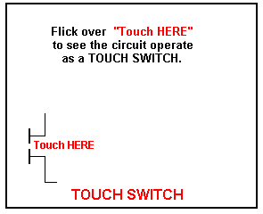
Flick over the TOUCH PADS very quickly to
see the circuit operate
FACTS TO REMEMBER:
Basically there are two different types of DIGITAL GATES: TTL and CMOS.
TTL gates have a very low input impedance (resistance) and CMOS has a very high
input impedance. The end result is they both work the same i.e. the
circuit has the same outcome, but the value of resistors and capacitors for the
biasing and timing components is completely different. The difference can be a
factor of 10 to 1,000 or more so you must design around "TTL"
or "CMOS" and you cannot replace a CMOS NAND gate, for
instance, with a TTL NAND gate without completely re-designing the surrounding
components.
TTL chips require a small amount of current to drive the internal circuitry.
CMOS chips require almost NO POWER to drive the internal circuitry. CMOS gates
require less than a fraction of a micro-amp. TTL requires a milliamp or more
for each gate.
When designing with CMOS gates, you can consider the input impedance of a gate
to be infinity. In other words the gate does not put any load on the
surrounding circuit.
In general, a gate changes state when the input voltage rises above about 55 -
65% of rail voltage. And when the voltage is falling, the gate changes at
approximately 45 - 35%.
If the voltage is rising or falling SLOWLY, the output of a gate can flutter
HIGH-LOW-HIGH-LOW during the time when the voltage is between 34 - 54%. This is
called the INDETERMINATE zone and the voltage should not be kept in this
region.
It takes a short period of time before a gate starts to flutter and
during normal operation the voltage changes from LOW to HIGH very quickly and
the gate does not have time to start to flutter.
In the Touch Switch circuit the voltage changes from one level to the other
quite slowly. When a finger is applied to the touch pads, the voltage on the
input of the first gate rises slowly in digital terms.
And the time-delay circuit raises the voltage on the second gate very slowly.
This may causes the gate to flutter and if this circuit is used to activate a
device such as counter module, it may produce false triggering.
Unless you know the quirks of digital chips, you will wonder where the false
triggering is coming from!
This is only a demonstration circuit and may produce multiple pulses.
WHY?
Why is it important to know how a circuit works?
The answer is simple. You may need to modify, adapt, or interface it to
another circuit. If you don't know how everything operates, it will be almost
impossible to connect the two circuits together.
For instance, you may want to increase the time-delay of the Touch Switch. For
this you need to know the components that create the delay (the 10u
electrolytic and 100k resistor). Once you know the components, you can
experiment with increasing or decreasing the values. You don't have to know the
mathematics to arrive at the time-interval as five minutes of experimenting
will produce the values but it is handy to know that increasing the value of
the capacitor or resistor (or both) will increase the time.
Why is the layout of a circuit so important?
All the circuits we present in this course follow a
very strict code of layout so their operation can be quickly worked out. That's
why we include all component values on the circuit. Anyone who draws a circuit
without including the component values has absolutely no electronics
appreciation at all.
Quite often the operation of a circuit is entirely dependent on the value of
the components and if they are missing, or contained in a list of parts, it
will take time to work out how the circuit works.
The whole idea of a circuit diagram is to be able to quickly work out if it is
doing what you want it to do. And to do this it must contain as much detail as
possible.
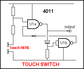
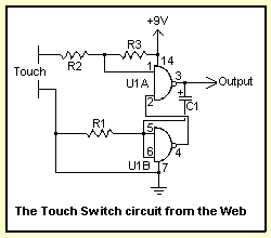 As an example, this Touch Switch
circuit is very hard to follow. The component values are not on the diagram and
the layout makes it difficult to see how the two gates are connected together.
If a circuit is laid out properly, you can "see" it working - just
like the animation we included above.
As an example, this Touch Switch
circuit is very hard to follow. The component values are not on the diagram and
the layout makes it difficult to see how the two gates are connected together.
If a circuit is laid out properly, you can "see" it working - just
like the animation we included above.
Keep this in mind when drawing diagrams. Keep them simple, clear and easy to
follow. This will help others to follow your circuits - especially when you
have designed something new.
The main fault with the diagram on the left is the feedback line (from pin 4 to
pin 2). It should be much clearer as it is extremely important in the
operation of the circuit. In our diagram above, we have placed the two gates
apart, with one gate feeding the other. Then the feedback line goes from the
output of the second gate to the input of the first. The line is also marked
with a "backward arrow" to emphasise the fact that signals on this
line are travelling backwards.
WHERE ARE WE GOING?
The main aim of this course is to get you
familiar with electronic components and "building blocks."
As far as gates are concerned, it is not necessary to go past the elementary
knowledge as any complex gating situations are best handled with a
microcontroller design.
This is the way we are heading with this course as electronics is changing
rapidly and for a few dollars you can get a
microcontroller chip that will take the place of dozens (if not hundreds) of
gates and do it all in an 8-pin chip!
It's all done by programming the chip and you can keep modifying the program
until it works perfectly, without having to connect lots of gates together or
even take up a soldering iron.
There are other advantages of a microcontroller.
It is much easier to interface
a microcontroller to the outside world than a digital chip. Everything on the
outside runs too slowly for digital IC's and they create the effect known as
FALSE TRIGGERING.
So, it's only the very elementary concepts of gating that are required
and when you have studied our PIC microcontroller section you will opt for a micro
design, EVERY TIME!
Some chips do not have the problem of "flutter" when the voltage is
rising and falling because they do not have an INDETERMINATE ZONE. They
have a circuit on each input line that prevents the gate from changing state
until the input voltage reaches exactly 66% of rail voltage. The input
voltage must then drop to exactly 33% for the output to change back to its
original state.
If the voltage swing is between 34% and 65%, the chip does not change state.
This circuit is called a SCHMITT TRIGGER and the gap between the high and low
trigger points is called the HYSTERESIS GAP.
This gap is not a problem when the chips are used in DIGITAL SITUATIONS as a
digital signal is required to rise to at least 85% of rail voltage and drop to
15%.Finally, a point to remember.
Many digital IC's are no longer manufactured, so keep this in mind when
designing a new project.
The NAND gate is called a "universal gate" as it can be converted
into all the other gates by simply wiring 1, 2, 3 or 4 NANDs together. This is
only suitable for demonstration purposes as the use of a whole chip for such a
simple operation is very wasteful.
NEXT
|