|

INDEX
Page 51
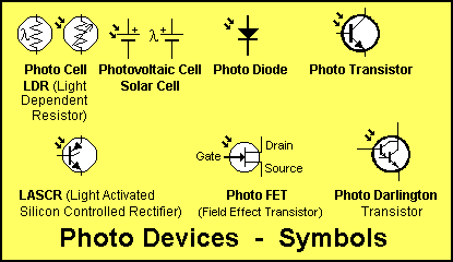
Photo Devices
The devices covered in this discussion are as follows: They are shown
in approximate increasing sensitivity. The Photo Cell is the least sensitive while the Photo Darlington is the
most sensitive:
The Photo Cell -
(Photo
resistor - LDR)
The LDR
(Light
Dependent Resistor - Photo Cell)
The Photovoltaic Cell - solar cell -
produces
an output voltage
The Photo Diode
The Photo Transistor
The Light Activated SCR
The Photo FET
The Photo Darlington Transistor
All the Photo Devices in the Circuit Symbols Library will be
described together in this article because they all do the same thing - detect
light. The diagram below shows the symbols of the devices we will cover:
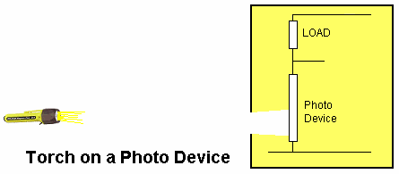
All Photo devices operate very similar to a variable resistor.
When they are receiving no illumination, they have a HIGH resistance.
When the illumination is
bright, they exhibit a LOW resistance.
The
diagram below shows how the circuit sees the Photo device. The output is
taken between the device and the load resistor. The load resistor can also
be called a "stop" resistor or "limit" resistor as it
limits the current taken by the device when it is detecting high
illumination.
Note: the output is shown to "fall" as the brightness increases.
This means the output voltage drops as the illumination increases and must
be detected by the next stage in the circuit. See Page
2 for for details.
The only way to work
out which device you need for a particular application is to build an
experimental circuit.
There is a wide variety of photo devices on the market but very few are
available at retail level and there is no way to compare the relative
sensitivity of each device, from the parameters supplied with each device. So
you have to carry out an actual physical test.
The simplest experimental circuit is to connect each device to the high-ohms
range of a multimeter. The diagram below shows this arrangement and how the
multimeter will react when the device detects light.
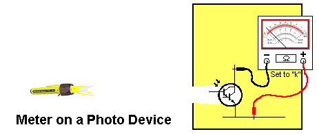
Note: The
multimeter is connected correctly because the negative
lead of the multimeter is connected to the positive of the battery inside
the meter.
There are basically three types of photo devices. Low
sensitivity, medium sensitivity and high sensitivity. The low-sensitivity
devices are the Photo Cell and Photo Diode. The medium sensitivity device is the
Photo Transistor and the high sensitivity devices are the LASCR, Photo FET and
Photo Darlington transistor. When comparing these three groups, you will
be able to see the relative movement of the needle.
TWO
CONDITIONS
Photo devices basically operate under two different conditions. Condition-one
is a change from dark to light (or light to dark. Condition-two
is a change from medium
illumination to
brighter illumination (or brighter to darker).
For the first condition, when the Photo device is connected to the multimeter, the needle will barely move when
it is in darkness and produce almost full-scale deflection in bright
light. In the second condition, the needle will sit somewhere on the scale
and move only a very small amount.
It will move very little for an LDR. It will produce a larger movement for
the Photo transistor and even more movement for the Photo Darlington transistor.
Depending on the amount of movement, you have the choice of using
an expensive high-sensitivity device or a low-sensitivity device with additional
gain being provided by an amplifying stage.
Sometimes the high-sensitivity device is cheaper than a low-sensitivity device,
so this will also influence your decision.
The end-result will depend on the suitability; the availability of the component
and the cost.
All the devices above produce no output voltage. They merely change in
resistance when light is detected. The only device that produces a voltage when
light is detected is the Photovoltaic Cell. It is a solar cell and
produces both a voltage and current when exposed to light. As the light intensity
increases, the voltage increases but the most important feature is the current.
When both a voltage and current are produced, the cell is said to be capable of
delivering ENERGY.
Individual solar cells can have a voltage output from 0.45v or greater (actually
almost any voltage). In actual fact, a number of pieces of semi-conductor
material are connected together in series/parallel within the cell, to produce
the output voltage and current.
Cells can also produce current outputs from a few milliamps to hundreds of
milliamps. This is due to the connection of many pieces of semi-conductor within the device.
The characteristics of each solar cell is provided at the time of
purchase.
A solar cell does not produce very much output (current output) under room
illumination and they are fairly large in size. This may influence your
decision for its use as a detector.
WHICH
TYPE DO I USE?
Due to the general lack of Photo devices in hobby outlets, the
circuit you choose will depend on the types available. For this reason we
cannot provide particular type numbers or specifications. All the circuits in
our discussion will
be of a general nature.
Sometimes it is cheaper to get a "hobby pack" of assorted types or go
to a surplus outlet, as some original types are very expensive.
These notes are designed to help you recognise "photo" transistors and
diodes and show typical circuits for their use.
One point to note is the number of leads on a photo device. Both
photo-transistors and photo-diodes can have two leads as the base of a photo
transistor is not connected to an outside circuit and thus it is not brought out
of the package. This makes it extremely difficult to tell the difference between
a photo diode and a photo transistor. In fact it is impossible without
testing its performance.
A photo transistor will be between 10 - 100 times more sensitive than a
photo diode.
THE
PHOTO
TRANSISTOR
The Photo transistor is an ordinary transistor in a clear plastic
case. If the case is
dark, the transistor will respond to infra-red light only - otherwise the device
can/will respond to both ordinary light and infrared light.
All transistors will respond to light and that is why
they have to be in a light-tight case if you don't want them
to respond to light. The silicon material making
up the junction of the transistor changes resistance when it sees
the energy from a light-source and this change is detected between
the collector and emitter leads.
Sometimes a second transistor is also mounted inside the case and
it amplifies the change in resistance to produce a more-sensitive
device. The combination is called a PHOTO-DARLINGTON
TRANSISTOR.
Two less-sensitive devices are also available. They are a
PHOTO-DIODE and PHOTO-RESISTOR (also called a LIGHT-DEPENDENT
RESISTOR - LDR).
Some devices detect visible light while others detect
infra-red.
Getting a photo-detecting circuit to work requires a little bit of
experimentation.
You need to determine if the device is sensitive enough for the
application and then adjust the circuit for the lighting
conditions.
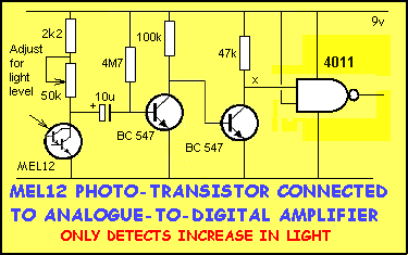
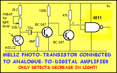
The circuit above can be adjusted so that
almost any light-level can be detected. When light is detected by
the MEL-12 photo-transistor, its resistance DECREASES. This means
the voltage-level sitting on the left-side of the 10u electrolytic
is brought down towards the 0v rail. This causes the right-side of
the electro to fall. The result is the voltage-level on the
base of the first transistor is REDUCED. This turns the transistor
OFF. The second transistor is turned ON and the voltage
at point "x" changes from a HIGH to a LOW. This voltage swing is
passed to the CD 4011 NAND gate to operate a further circuit.
The 50k mini-trim pot
changes the gain of the photo-transistor. It makes the
transistor
more-sensitive
as the resistance of the pot is decreased. The result is the
voltage-fall on the left-side of the 10u electrolytic is greater for
any given change in light and this means a very small change in
light-level will cause the circuit to operate.
The circuit will only detect AN INCREASE IN LIGHT. When the
light-source is removed or reduced, the circuit does not respond.
The circuit below is designed to detect when the light-source turns OFF:
In the following circuit, the A-to-D stage and 4011 NAND gate
have been replaced by a Schmitt Trigger.
The MEL-12 Darlington Photo-transistor is connected directly
to the input of the Schmitt gate and the circuit can be adjusted via
the 50k mini-trim pot.
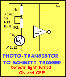
When the MEL-12 receives light, the voltage on the input of the
Schmitt gate drops from a HIGH value to a LOW value. For the circuit
to work, the LOW value must be 33% of rail voltage or less.
When a light-source is removed from a MEL-12, the voltage on the
input of the Schmitt gate rises to a HIGH value. For the gate to
change state, the voltage must rise to 66% of rail voltage or
higher.
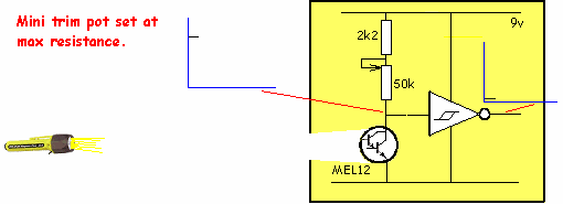
The animation below shows how the mini-trim pot changes the gain of
the photo-transistor.
If the change in light intensity is not sufficient to operate the
Schmitt gate, you can add the A-to-D stage described above
and the 10u electrolytic.
NEXT
|