|
|
THE 555 IC

|
|
Page 1 |
CHIP
PRICES
|
|
Contents:
Amplifier (555)
- Page 3
Bicycle Light
- Page 3
Dark Detector - Page
3
Driving high currents -
Page 3
555 timer IC - Page 1
Inside the 555 chip - Page 1
Flashing Indicators
- Page 3
Flip Flop - Page 3
Function of each pin - Page 1
Gating the Oscillator - Page 2 & 3
How the 555 oscillates - Page 1
IR Transmitter - Page 3
Knight Rider - Page 3
Light Detector - Page 3
Mark-Space ratio - Page 2
Negative Supply - Page 3
One-shot negative trigger - Page 1
One-shot positive trigger - Page 1 & 3
Police Siren - Page 3
Pulse Generator - Page 2
Schmitt Trigger - Page 3
Substituting a 555 - Page 2
Touch Switch - Page 3
Using the 555 - Page 1
1.5v LED Flasher - Page 3
555 Vs 7555 - Page 1
555 as a monostable - Page 1
555 as an oscillator - Page 1
555 Calculator (oscillator) - Page2
555 Oscillator - Page 2
555 as a Delay - Page 3
556 - Page 2
7555 - Page 1 |
|
The 555 IC is one of the
simplest and most rugged IC's on the market. It has been used in thousands of
applications and is extremely popular. This discussion will cover its numerous
modes of operation and present a number of circuits for these
applications.
However I must point out one thing.
The 555 is not suited for battery applications and it is not really suited for
combining with some types of CMOS circuitry. The 555 is a very noisy chip and
has a very nasty internal feature called "crow-bar effect" that can
put a lot of noise on the power rails of a circuit.
Its operation as an oscillator can be done
by other chips and we have provided some alternatives in the notes. The 555 has
a number of derivatives that offer improvements (such as low-power, low
voltage, high speed operation) and these will also be covered.
This is the first time a number of comparisons and alternatives have been provided in a
discussion and this is needed for you to get a complete picture of its
suitability for a particular project. There are cheaper and
better chips to carry out identical operations to a 555 and we will leave it to
you to decide.
THE 555 TIMER IC
The 555 is commonly called a TIMER IC. It is an 8-pin chip and has
a number of different identifications: LM555CN from
National and SE555/NE555 from Signetics are just two manufacturers. These numbers all refer to the
most common and cheapest version, we will call the 555.
The 555 contains more than 28 transistors and it is basically a chip containing
a number of building blocks that end up very similar to an oscillator without
the TIMING COMPONENTS. It needs two or three external components to produce
an oscillator capable of operating at a frequency from 1Hz to 500kHz. When it
oscillates at a frequency less than 1Hz, the circuit is called a Timer or
Delay. The chip also has a pin (pin 2) that prevents the chip from starting the
Timing cycle until it is taken LOW. Another pin (pin 4) stops the chip from
oscillating (or continuing with a delay-time) when it is taken LOW and a pin
(pin 5) that can adjust the mark-space ratio of the waveform.
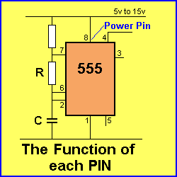
The diagrams below show the names of each pin and a simplified block diagram of
the internal workings.
The 555
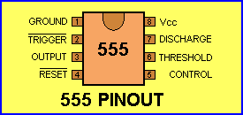
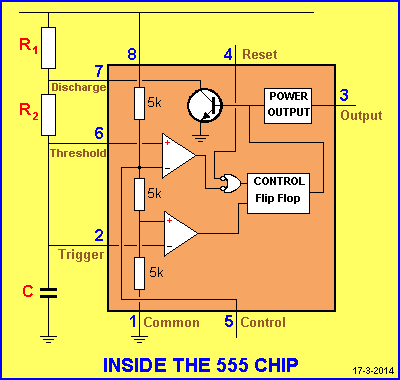
THE FUNCTION OF EACH PIN
Pin 1 Ground
The ground (or common) pin is connected to the 0v rail -
commonly called the negative rail or EARTH rail.
Pin 2 Trigger
This pin connects to the lower comparator and is used to set the control flip
flop. When it is taken LOW, it causes the output
to go HIGH. This is the beginning of the timing sequence for a monostable
operation. Triggering is accomplished by taking the pin below 1/3 of rail
voltage - in digital terms, this is called a LOW. The action of the trigger input is level-sensitive, allowing slow
rate-of-change waveforms, (as well as pulses), to be used as trigger sources. The
trigger pulse must be of shorter duration than the time interval determined by external R and C. If this pin is held low
for a longer period of time, the output will
remain high until the trigger input is high again.
If the trigger input remains
lower than 1/3 rail voltage for longer than the timing cycle, the timer will
re-trigger
upon termination of
the first output pulse. When the timer is used in monostable mode
with trigger pulses longer than the output pulse, the trigger duration must be shortened by
external circuitry.
The minimum
pulse-width for reliable triggering is about 10uS.
If this pin is kept LOW, the output remains HIGH and a high on pin 6
(Threshold) will not force the output LOW. In other words the
trigger pin is the dominant pin.
Pin 3 Output
The output of the 555 comes from a high-current
totem-pole stage. This provides both sinking and sourcing current. The high-state output voltage
is about 1.7 volts less than the supply.
At 15 volt supply, the chip can sink 200mA with an output-low voltage level of 2 volts.
High-state level is 13.3 volts. Both rise and fall times of the output waveform are quite fast,
typical switching being 100nS.
To make the output HIGH, the TRIGGER PIN (pin 2) is momentarily taken from a
HIGH to a LOW. This causes the output to go HIGH. This is the only way
the output can be made to go high.
The output can be returned to a LOW by making the THRESHOLD PIN (Pin 6) go from a
LOW to a HIGH.
The output can also be made to go LOW by taking the
RESET PIN to a LOW state.
Pin 4 Reset
This pin is used to make the OUTPUT PIN (Pin 3) LOW. The reset pin must
go below 0.7 volt and it needs 0.1mA to reset the chip.
The
RESET PIN is an overriding function. It will force the OUTPUT PIN to go LOW regardless of the
state of the TRIGGER PIN (Pin 2). It can be used to terminate an output
pulse prematurely, to gate oscillations from "on" to "off." The pin is
active when a voltage level between 0v and 0.4 volt is applied to
it. When not used, it is recommended that the RESET PIN be tied to the
positive rail to avoid the possibility of false
resetting.
Pin 5 Control Voltage
This pin allows direct access to the 2/3 voltage-divider point. This is the reference level for the upper comparator.
When the 555 timer is used in a voltage-controlled mode,
the voltage-controlled operation ranges from about 1 volt below rail-voltage to
2 volts above ground (0v). Voltages can be
safely applied outside these limits, but they should be confined to between 0v
and rail
voltage.
By applying a voltage to this pin,
it is possible to vary the timing of the chip independently of the RC network.
The control voltage may be varied from 45 to 90% of the Vcc in the monostable
mode, making it possible to control the width of the output pulse independently
of RC. When used in the astable mode, the control voltage can be varied
from 1.7v to the full Vcc. Varying the voltage in the astable mode will produce
a frequency modulated (FM) output.
If the control-voltage pin is
not used, it should be bypassed to ground, with a 10n capacitor to prevent noise
entering the chip.
Pin 6 Threshold
Pin 6 is one input to the
upper comparator (the other is pin 5). It makes the OUTPUT PIN go LOW.
To
make the output go LOW, the Threshold pin is taken from a LOW to a level
above 2/3 of rail voltage. This pin is level-sensitive, allowing
slow rate-of-change waveforms to be detected.
A dc current, termed the
threshold current, must also flow into this pin from the external
circuit. This current is typically 0.1µA, and will determine the upper limit of
total resistance allowable from pin 6 to rail. For 5v operation the resistance
is 16M. For 15v
operation, the maximum resistance is 20M.
Pin 7 Discharge
This pin is
connected to the open collector of an NPN transistor. The emitter
goes to ground. When the transistor is turned "on,'" pin 7 is effectively
shorted to ground. The timing capacitor is connected between pin 7 and
ground and is discharged when the transistor turns "on". The conduction state of
this transistor is identical in timing to that of the output stage. It is "on"
(low resistance to ground) when the output is LOW and "off" (high resistance to
ground) when the output is HIGH.
Maximum
collector current is internally limited by design, so that any size capacitor
can be used without damage to the chip. In certain applications,
this open collector output can be used as an auxiliary output terminal, with
current-sinking capability similar to the OUTPUT (pin 3).
Pin 8 Rail
This pin (also
referred to as Vcc) is the positive supply voltage pin for the 555.
Supply-voltage operating range is +4.5 volts to +16 volts.
The chip will operate over this voltage range without
change in timing period. The only change is the output drive capability, which increases
in current as the supply voltage is increased.
USING THE 555
A 555 can be wired:
1. As a TIMER (monostable operation - also called
a DELAY),
2. As an OSCILLATOR (also called a MULTIVIBRATOR - or astable operation)
3. As a ONE-SHOT (also called monostable operation).
The 555 IC is an extremely popular IC. It is simple to use and very rugged.
It comes in a single, dual or quad package with part numbers such as LM555, NE555, LM556,
NE556. It is ideal
for astable (free-running) oscillators as well as the one-shot monostable
mode.
The 555 can be triggered and reset on
falling waveforms and the output can source or sink up to 200mA. The HIGH
output is about 1.7v less than supply. The NE555 operates 3v - 16v DC.
Maximum
operating
frequency is 500kHz.
THE 7555
7555 is a CMOS version of the 555.
It is exactly the same as the 555 but consumes less power. The 555 consumes
10mA, while the 7555 consumes 80uA (1/120th). The CMOS version comes with different identifications according to the
manufacturer.
LMC555 or LM555CN is made by National Semiconductors, TLC555 is made by Texas
Instruments, ICM7555 is supplied by Philips, ZSCT1555
comes from Zetex and ICM7555 is made by Maxim. The main feature to note
is the inclusion of the number "7" or the letter "C" to
identify the CMOS version.
They use less power than
the older (555, NE555, LM555) versions and don't require a capacitor on
the control pin. Although pin and functionally compatible, the component
values differ between the low-power CMOS and older versions.
The Exar XR-L555 timer is a micro-power
version of the standard 555 offering a direct, pin-for-pin substitute with
the advantage of lower power operation.
It is capable of operation from 2.7v to 18v. At 5v, the
L555 will consume about 900 microwatts, making it ideally
suitable for battery operated circuits. The internal schematic of the L555 is similar to the standard 555 but with
current-spiking filtering, lower output drive capability, higher nodal impedances, and
better noise reduction system.
USING THE 7555
The ICM7555 is a CMOS timer providing significantly improved performance
over the standard NE/SE555 timer, while at the same time being a direct
replacement in most applications.
Improved parameters include
low supply current, wide operating supply voltage range, low THRESHOLD,
TRIGGER, and RESET currents, no crow-barring of the supply current during output
transitions, higher frequency performance and no requirement to decouple
CONTROL VOLTAGE for stable operation.
The ICM7555 is a stable controller capable of producing accurate time delays
or frequencies.
In the one-shot mode, the pulse width of each duration is precisely
controlled by one external resistor and capacitor.
For astable operation as an
oscillator, the free-running frequency and the duty cycle are both accurately
controlled by two external resistors and one capacitor. Unlike the bipolar 555
device, the CONTROL VOLTAGE pin does not have to be decoupled with a capacitor.
The output can source or
sink currents large enough to drive TTL loads or provide minimal offsets to
drive CMOS loads.
Maximum output current 50 - 80mA.
- Exact equivalent in most applications for NE/SE555
- Low supply current: 80µA (typical)
- Extremely low trigger, threshold, and reset currents: 20pA (typical)
- High-speed operation: 500kHz guaranteed
- Wide operating supply voltage: 3v to 16v
- Normal reset function. No crow-barring of supply during output transition
- Can be used with higher-impedance timing elements than the bipolar 555 for
longer time constants
- Timing from microseconds to hours
- Operates in both astable and monostable modes
- Adjustable duty cycle
- Output source/sink driver can drive TTL/CMOS.
Maximum output current 50 - 80mA.
Typical temperature stability of 0.005%/°C at 25°C
Rail-to-rail outputs
An improvement on the CMOS 7555 is the ZSCT1555 from Zetex. It is
guaranteed to work down to to 0.9 volts with bipolar technology. It has been
designed for portable
applications, by offering single battery cell operation. ( See
end of P3 for a technician's difficulty with getting this chip to oscillate.)
It provides the same precision timing capabilities as its
predecessors, (the 555 and 7555) it has the same 8 legged pin-out. With the
simple adjustment of external passive components to set the frequency, the
device's function is just the same, whether it be generating accurate time
delays or oscillations.
Assuming a 5v supply, a typical CMOS part draws 170uA
while the new timer
pulls 140uA, and at 1.5v just 75uA.
555 Vs 7555
The choice between the standard 555 and CMOS version (7555) or ZSCT1555 will depend on
cost, availability, load current required and frequency of operation. It will mainly
come down to battery or mains operation for the project.
Normally, when we change from a TTL chip to a CMOS chip, the component values
change by a factor of 10x or 100x. This is because the TTL chips are very low
impedance and CMOS is very high impedance.
But if a 555 is substituted for a CMOS version, the timing components remain
the SAME!
This is very convenient. Chips can be substituted without having to alter the
surrounding circuitry. The only change will be the current consumption of the
chip. In general, the consumption will reduce from about 10mA to approx 0.5mA.
(A LED Voltmeter circuit made the following circuit-current comparison: using
555 = 7mA, using 7555 = 0.35mA). This is typical of the current-saving of a
CMOS version.
This article covers most types and provides a number of comparisons and
substitutions.
A typical 7555 circuit is shown below: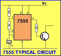
Note the need for the driver transistor in the circuit above,
as the 7555 has an output capability of about 50mA.
DRAWING 555 "BLOCKS"
One of the most important points when drawing a 555 "block" is maintaining
a standard layout. Diagrammatic blocks
on a circuit diagram are not supposed to show the pins in the same order as the
legs on a chip. The wiring to the chip should be placed in positions to represent
their function. The power is placed at the top, ground at he bottom,
input at the left and output at the right. The other lines are also placed in
appropriate positions.
The layout should be positioned to aid in the interpretation of a diagram. The
end result should be to provide the maximum information and make it easy to
interpret the symbol.
Many of the 555 circuit diagrams place the lines to the 555 block so you have
to interpret every diagram individually. This makes reading a circuit diagram
very slow.
The first thing you need to know is the function of each pin. See the animation
below:
The 555 can be used for a number of applications.
It can be wired as an OSCILLATOR or a MONOSTABLE or DELAY and many different circuits
can be produced with these modes of operation.
THE 555 AS AN OSCILLATOR
The 555 can be wired as an OSCILLATOR. It needs 2 external components - a resistor
R
and a capacitor C. These are called
TIMING COMPONENTS. The diagram below shows these two components:
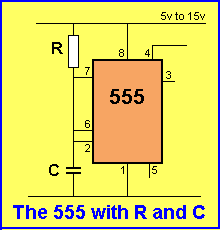
The
capacitor charges via R
and when it reaches 2/3 of rail voltage, pin 7 shorts
the capacitor to ground. This means the capacitor charges slowly but discharges
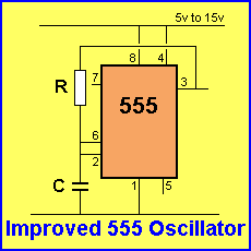
very quickly. An improved layout is shown below:
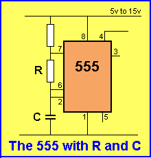
The
capacitor charges via R (plus the top resistor) and discharges via R (only). If
the top resistor is small compared with R, we can neglect it, so that
C
charges via R and discharges via R
at about the same
rate.
The top resistor simply
separates pin 7 from the positive rail as pin 7 shorts to ground to discharge
the capacitor during part of the cycle.
HOW THE 555 OSCILLATES
The capacitor charges via the timing resistor
R
and when the voltage across it reaches 2/3 of the supply voltage, the output of the 555 goes
LOW. The timing resistor is taken to the 0v rail via pin 7 and the capacitor discharges.
When the voltage across the capacitor reaches 1/3 of rail voltage the output of
the 555 goes HIGH. The timing resistor is taken to the positive rail
via the top resistor (pin7 effectively comes out of circuit) and the
cycle repeats. Don't worry about pins 4 or 5 at the moment.
The animation below shows how the 555 oscillates:
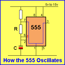
These are the three points to note:
1. Pin 2 detect the low voltage on the capacitor, and makes pin 7 and the output go
HIGH
2. Pin 6 detects the high voltage on the capacitor and makes pin 7 and the output go LOW
3. Pin 7 is "in-phase" with the output. (both are low at the same
time)
An improved oscillator is shown in the diagram below. It uses only one resistor
to charge and discharge the capacitor and the circuit does not have the
wasteful top resistor. The circuit draws less current than the circuit above
but the only difference is the frequency of operation will be lower for the
same value of components because the voltage delivered by the output line is
1.7v less than the supply rail. The output can deliver up to 200mA but if it is
delivering a high current, the output voltage may be reduced and this will
affect the frequency of operation. If a reliable frequency is needed, this is
not the circuit to choose.
THE
ACTION OF PIN 4
Pin 4 is called the RESET PIN. It is called an ACTIVE LOW pin.
When pin 4 is HIGH, the chip operates normally. When pin 4 is taken LOW,
the output of the chip is INHIBITED - it remains LOW. Pin 7 is
also taken low and the chip is prevented from oscillating.
Mouseover the following animation to see the action of pin 4:
Mouse-over to INHIBIT the 555
THE
555 AS A MONOSTABLE
The 555 can be wired as a monostable. A monostable has one stable state and
that is the OFF state. The unstable state is called the ON or HIGH state.
When it is
triggered by an input pulse, the monostable switches to its temporary or ON state. It
remains in that state for a period of time determined by an RC network and returns
to its stable state. In other words, the monostable circuit generates a
single pulse of a fixed time duration each time it receives and input trigger
pulse.
The monostable circuit can also be called a ONE-SHOT due to the single-pulse
it creates. This type of circuit can be used for activating an external device
for a specific length of time. They can also be used to generate delays.
Another use for this type of circuit is to take the brief pulse of a
push-button and activate a device. This is called a PULSE-EXTENDER.
It can also be used to clean-up the noisy output of a push-button and this is
called SWITCH DEBOUNCING.
The diagram below shows a push-button connected to a 555. When the button is
pressed, the relay operates for 5 seconds. The button must be released before
the time-interval has expired otherwise the time is extended. This is the only
limitation of this circuit.
The next circuit
is an improved design. The switch can be pressed for any length of time and the
circuit will only produce a 5 second output. The circuit is prevented from
re-triggering by the addition of a 470k and 100n capacitor. When the switch is
pressed, the uncharged capacitor takes pin 2 low and triggers the
circuit. If the button is kept pressed the 100n charges and takes pin 2
high. The potential across the voltage divider formed by the 47k and 470k resistors is insufficient to
re-trigger the monostable. The circuit "times-out" and the output
goes low. When the button is released, the 100n discharges through the 470k and
is ready for the next press.
A monostable (one-shot) can be connected to an astable
(free-running oscillator) so that it gates (or inhibits) the oscillator to
produce an output tone for a short duration. The circuit below can be used
for an application such as doorbell. It is not suitable for battery operation
as the 555 IC's are connected to the supply and draw current at all
times.
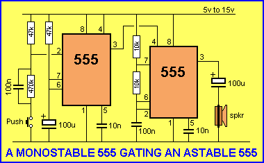
This circuit can be used
for a doorbell.
Pin 2 of the first 555 is HIGH and thus it is
"non-operational" as it detects a LOW. Pin 6 is detecting a HIGH and
thus the output of the IC is LOW. The output of the first 555 goes to the
INHIBIT pin of the second 555. When pin 4 is LOW, the output of the chip is kept
LOW.
HOW THE 555
WORKS
Here's a circuit to help you understand how
the 555 works.
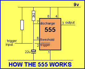
In the circuit above, the trigger input is HIGH
and a 22u and 2k2 are connected to the chip.
When the power is connected, the trigger input will be high and the
threshold line will be low. The internal circuitry of the chip will cause it
to produce a HIGH and the Discharge pin will be effectively not connected.
The 22u will charge via the 2k2 and when pin 6 (threshold) sees 2/3 rail
voltage, the output goes LOW and the discharge pin goes LOW and discharges
the 22u.
This is how the chip sits.
If the trigger input goes low for a short period of time, the output pin
goes HIGH and the discharge pin goes high and the22u charges. When the
threshold pin sees 2/3 rail voltage the output pin goes LOW and the chip
remains in this state.
If the trigger line remains LOW, the output pin remains HIGH as the trigger
pin controls the state of the output. The 22u will be fully charged and the
chip will change state immediately the trigger line goes high.
NORMALLY CLOSED TRIGGER
Here is a circuit that uses the features we
have just discussed:
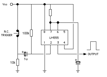
Normally-closed trigger
Here is the circuit rearranged so that the function of the pins are obvious.
A circuit diagram does not follow the pin-out of the chip, (that's the
function of a wiring diagram). A circuit diagram conforms to the functions
of the chip.
ONE-SHOT USING A
NORMALLY-CLOSED SWITCH
In the circuit above, the trigger input (pin 2) is HIGH and a 22u and 100k are
connected to the threshold pin (pin 6) of the chip.
When the power is connected, the trigger input will be high and the
threshold line will be low. The internal circuitry of the chip will cause it
to produce a HIGH and the Discharge pin will be effectively not connected.
The 22u will charge via the 100k and when pin 6 (threshold) sees 2/3 rail
voltage, the output goes LOW and the discharge pin goes LOW and discharges
the 22u.
This is how the chip sits – with the 22u discharged.
If the n.c. switch opens, the trigger input goes low. The output pin goes
HIGH, the discharge pin goes high (it actually goes to a condition of
high-impedance – or more accurately it goes to a state where it disconnects
from the 100k and 22u) and the 22u charges via the 100k. When the threshold
pin sees 2/3 rail voltage the output pin goes LOW and the chip remains in
this state.
If the trigger line remains LOW, the output pin remains HIGH as the trigger
pin controls the state of the output. This is most important to remember.
But in our case the trigger line is connected via a 1u capacitor and it does
not remain low. It has a short low period as determined by the timing of the
10k, 1u and 100k and ideally this low period is shorter than the timing on
pin 6.
If the switch is kept open, the 1u will charge and it will take a short
period of time for pin 2 to see a voltage 2/3 of rail voltage. Providing
this time is shorter than the time-delay created by the 22u and 100k (it
is), the timing will depend on the 22u and 100k, otherwise the 10k, 1u and
100k will create the time-delay.
To explain the trigger-line again:
When the switch is opened, the 1u will have no voltage across it (as it is
discharged by the 100k when the switch is closed) and the 100k and 10k will
form a voltage divider of approx 10:1 so that pin 2 will see a voltage less
than 1v. This will start the time-delay of the chip and the 1u will charge
via the 10k and 100k so that the voltage on pin 2 will rise at a rate
allowed by these resistors. This means pin 2 (which is the CONTROLLER of the
chip!!) will be at its high value VERY QUICKLY and will no longer control
the chip. The chip will now be looking for a HIGH on the threshold line to
perform the next part of the sequence.
If we keep pin 2 LOW for an extended period of time, the output will
immediately go HIGH. Pin 7 will immediately go open (it was previously LOW
and drawing current through the resistor connected between pin 7 and rail)
and the cap will charge. When pin 6 sees 2/3Vcc it will try to make the
output go LOW but pin 2 will keep it HIGH.
If pin 2 is taken HIGH, the output will go LOW immediately.
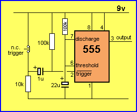
ONE-SHOT USING A
NEGATIVE-GOING TRIGGER
ONE-SHOT USING A
NEGATIVE-GOING TRIGGER
The circuit above shows the 555 with a
discharged 22u. The discharge pin will be connected to 0v and the output
will be LOW. When the negative-going trigger pulse is detected by pin 2, the
discharge pin (pin7) "opens" and the 22u is charged via the 100k. At the
same time pin 3 goes HIGH. The threshold pin (pin 6) detects when the
voltage on the 22u is 2/3Vcc and makes the output pin 3 LOW. The trigger
pulse must be shorter than the delay-time for this sequence to work.
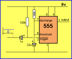
ONE-SHOT USING A POSITIVE-GOING TRIGGER
ONE-SHOT USING A POSITIVE-GOING
TRIGGER
If a positive-going trigger pulse is available, the above circuit can be
used.
P 2
|