|
|
|
|
THE 555 IC

|
|
Page 2 |
|
|
|
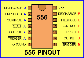
THE
556
The 556 is a DUAL 555.
It contains two identical 555 timer circuits.
The NE556/SE556 timers can be directly replaced by the CMOS types MC3456/MC3556.
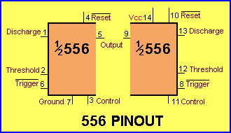
The following three pin-outs identify the 556 dual timer IC and the function
of each pin.
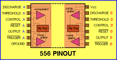
Discharge
is "in-phase" with the Output. (both are low at the same
time)
Threshold
detects the high voltage on the capacitor and makes
Discharge and
Output
go LOW
Trigger
detect the low voltage on the
capacitor and makes Discharge
and Output
go
HIGH
HIGH Interval (T1)
= 0.693 x (R1+R2) x C
LOW Interval (T2) =
0.693 x R2 x C
Frequency = 1.44 / ( (R1+R2+R2)
x C)
HOW TO USE THE CALCULATOR
Enter values for R1, R2, and C and press Calculate to determine HIGH
interval and LOW interval. For example, a 10k (R1), 100k
(R2) and 100n will produce output time
intervals of 7.62mS HIGH and 6.93mS LOW. The frequency will be about
70Hz
and a Delay of 0.01sec. R1
should be greater than 1k and C should be greater than 50p.
SUBSTITUTING A 555
A 555 (and the 556 varieties) can be replaced by low-power 555's
such as TLC555, LMC555, ICM7555. This has been covered above.
In this section we will show how to replace any of the 555 or 7555 devices with
a building block called a SCHMITT TRIGGER. The Schmitt Trigger chip we suggest is a 74c14 (40106 -CD 40106).
This chip contains six Schmitt Triggers.
It allows up to 6 building blocks to be created, similar to the
capabilities of a 555.
This is a much-more economical and
professional way to designing a circuit and two other
very important features are also provided.
The Schmitt Trigger consumes less current
and battery designs can be created.
A Schmitt Trigger does not put noise on the power rails of a project and
it can be used with other digital blocks without creating interference
problems.
Six gates in a single
hex Schmitt trigger chip allows the designer to produce 6 different building
blocks and quite complex circuits can be produced.
The type of 555 circuit we are suggesting be replaced with a Schmitt design is
one that meets one of more of the following criteria:
1. A design that needs to be upgraded and improved in
"professionalism."
2. A design that needs to be reduced in quiescent current,
3. A design that uses more than one 555
4. A design that employs 555 IC's with digital IC's.
A simple 555 design for a car, for example, does not need to be converted.
THE 555 OSCILLATOR
The following diagrams show a free-running 555 oscillator and its Schmitt
Trigger equivalent.
The circuit can be called an OSCILLATOR, SQUARE-WAVE OSCILLATOR or FREE-RUNNING
OSCILLATOR.
The 555 can sink or source 200mA and the two diagrams show this:
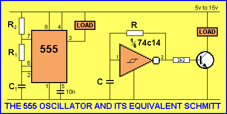
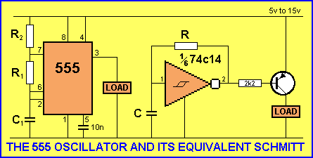
The only difference between the two circuits is the Schmitt
version will draw about 10mA -15mA less.
The 555 draws about 10mA for its internal operation and about 1mA - 5mA will be
"wasted" through R2.
If the load is less than 25mA, the following circuits can be used:
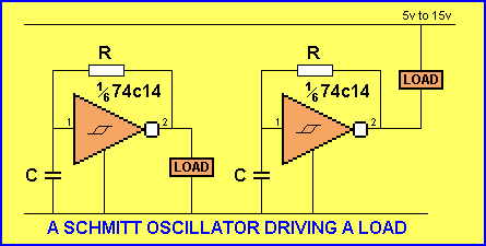
The output of a single Schmitt Oscillator will drive a load up
to 25mA, depending on the frequency of oscillation and the voltage of the
supply. As the voltage decreases, the load current reduces. At 5v, the load
will be a maximum of 10mA.
As the load current increases, the output will not rise to 66% of rail voltage
and the oscillator will "freeze."
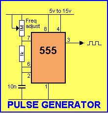
PULSE
GENERATOR
Another name for "oscillator" is PULSE GENERATOR. The following
circuit shows a 555 wired as a square-wave oscillator called a MULTIVIBRATOR.
The output waveform is adjustable and is ideal for injecting into RF and IF
stages. The square-wave is rich in harmonics and will pass through both RF and
IF stages to produce a tone or "buzz" in the speaker.
CHANGING
THE MARK-SPACE RATIO
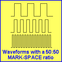
The MARK and SPACE are the HIGH and LOW values
of a waveform. When a waveform is HIGH, it is called the MARK.
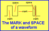
The
diagram above shows MARK and SPACE durations of different
lengths. Marks and spaces can be any length and can change during the
production of a waveform. If the length of the mark is equal to the space,
the waveform is said to have a 50:50 Mark:Space ratio, as shown below:
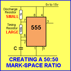
 A
waveform with a 50:50 Mark:Space ratio is produced by a 555 when the top
resistor (called the DISCHARGE resistor) is very small compared to
the TIMING resistor. This is shown in the diagram below:
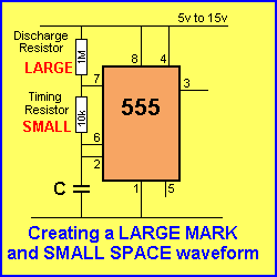
To
increase the MARK, the Discharge resistor must be LARGE compared to the
Timing resistor.
To
increase the SPACE, a diode is needed as shown in the diagram below: 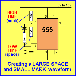
The MARK:SPACE ratio can be adjusted without altering the
frequency by connecting two diodes as shown in the diagram below:
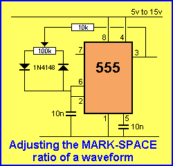
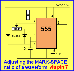 The two circuits above adjust the output from about 3% to 97% at a
frequency of approximately 1kHz.
You can use either pin 3 or pin 7 as they are "in phase" with each other.
Pin 7 needs a pull-up resistor as the transistor connected to this pin is in
an open-collector configuration.
GATING THE
OSCILLATOR
The 555 oscillator can be turned on and off via a control line. This is called
"Gating the Oscillator" or "Controlling the Oscillator."
When designing this type of circuit, two things need to be considered:
1. The oscillator to be switched off with the output HIGH
2. The oscillator to be switched off with the output LOW
The next consideration is:
3. The oscillator (block) to be switched off
4. The oscillator (block) to remain in circuit.
There is an enormous difference between these designs. The main difference is
the current consumption of the load, but the actual consumption of the chip can
also be important.
Take for example, these two circuits:
In the first
circuit, the key is in the output and the chip draws current all the time. If
the project is battery operated, it will need an on-off switch. The second
circuit uses the key as the switch and the circuit will not need a switch. The difference
is only 10mA but if the first circuit is left on, the battery will be dead in a
few weeks.
P 3
|
|