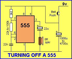
The next circuit shows one way to turn off a 555 after a period of activation:

The only problem
with this circuit is the gradual lowering in volume as the electrolytic
discharges. The 1,000u to 4700u determines the length of time the circuit is
activated AFTER the Bell-Push is pressed. The circuit drops to zero current
(the only current is the leakage of the 1,000u electrolytic).
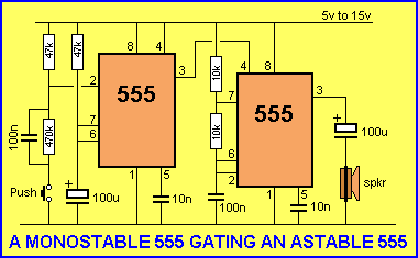
In the following circuit the first 555 gates the second 555.

The second 555 is
not turned off. The circuit inside both 555's are always drawing current.
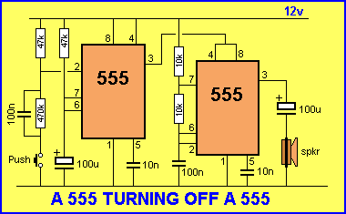
It is not practical to "turn off" a 555 as shown in the next diagram:

The output of a 555
is 1.7v less than rail voltage. This means the second 555 is receiving 10.3v
from the output line of the first 555 if the rail voltage is 12v. The maximum
output of the second 555 will be 10.3 - 1.7 = 8.6v This may be too low for many output
devices and the result may be disappointing.
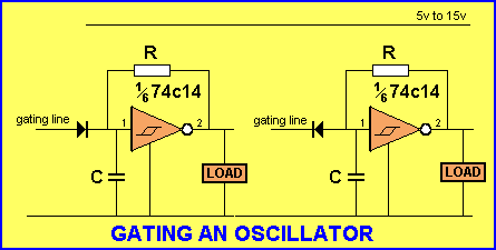
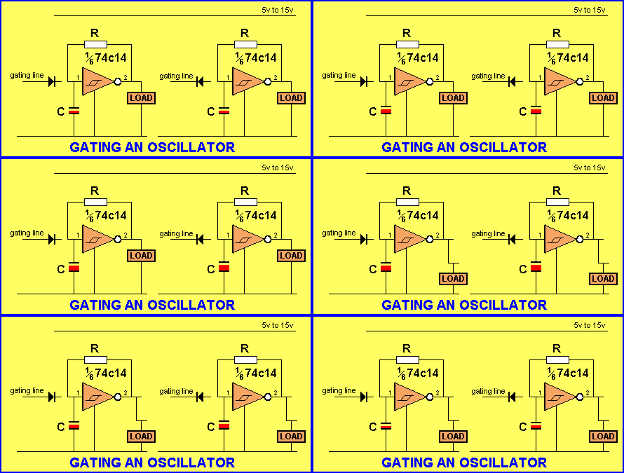
The Schmitt Trigger can be gated too.
The first point to note is the hex Schmitt trigger IC contains 6 identical
gates and the chip is normally permanently connected to the supply rail. If any
of the unused inputs are tied HIGH, the particular gate draws very little
current (less than 1uA), making the total for the chip about 6uA.
There are two ways to GATE a Schmitt Trigger and prevent it from
oscillating.
The diagrams below show a Schmitt Trigger being gated so that the output is:
1. LOW,
2. HIGH.

Mouseover the animations below and see how the GATING LINE
inhibits the oscillator:

Mouse-over to INHIBIT the Left Oscillator
For the left circuit, if the gating diode is taken HIGH,
the capacitor charges quickly. This inhibits the operation of the oscillator
and the output goes LOW. If a load is connected to the output of this gate, it will
not be driven and the gate will consume the least current.
For the right circuit, when the gating diode is taken HIGH it does not have any
effect on the operation of the circuit and the oscillator continues to operate.

Mouse-over to INHIBIT the Right Oscillator
For the left circuit, if the gating diode is taken LOW, it does not have any
effect on the operation of the circuit and the oscillator continues to operate.
For the right circuit, if the gating diode is taken LOW, the capacitor is
discharged and the oscillator is INHIBITED. The output goes HIGH and the load will be
driven. The circuit will draw maximum current.
If NO LOAD is connected to the output, an inhibited gate will draw more current
than when it is oscillating. Both arrangements will draw a similar current when
inhibited. The current taken will be about 1uA for the gate plus the
current through R.
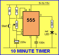
THE 555 AS A DELAY
The 555 can be used as a timer up to 10 minutes. This circuit is also called a
DELAY.
To start timing, the START button is pressed briefly and the output of the chip
goes LOW. At the expiration of 10 minutes, the output goes HIGH and the red LED
illuminates.
A simple application may be for a cooking operation in a shop.
If a product needs to be cooked or heated etc, the button can be pressed and
the LED illuminates when the time has expired.

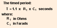
When
calculating the time-duration for the circuit above, the capacitor charges
from 0v to 2/3 rail voltage.

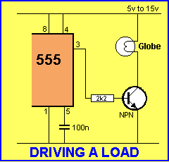
DRIVING
HIGH-CURRENT LOADS
The output drive-current for a
555 is 200mA maximum. The output voltage is 1.7v less than rail voltage.
A driver transistor can be connected to the output pin to improve the output
current to 1amp (or more) and deliver an output voltage that is near rail
voltage. Globes are a typical example of a high-current load. They require up
to 6 times the normal current when starting. This is due to the cold filament
having a very low resistance. The same applies to motors. They have a high
start-up current requirement.
Any driver transistor can be fitted as shown in the diagram below:

Use a driver transistor for loads greater than 200mA
The CMOS 7555 has an output current capability of 50mA and will
need a driver transistor for currents above 80mA.
MISTAKES
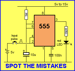
Here are some mistakes in a 555 circuit. They are "technical." Can you
spot them?

1.
Pin 2 must be taken LOW for it to activate the 555. The circuit shows a positive
voltage being applied to pin 2. This will do nothing.
2. Connecting pin 2 to pin 4 and leaving them "open" as shown in the
diagram above is very dangerous. These are fairly high-impedance pins and the
consequences of leaving them open will be unpredictable.
3. Pin 2 cannot be left "open." The 10u will initially charge to
2/3 rail voltage and the voltage will be detected by pin 6. Pin 7 will then
discharge the 10u and wait for a low to be detected by pin 2. Pin 2 will
actually have no voltage on it but the pin requires a very small current (about
500 nano-amp) to activate the chip. If a static charge delivers this
current, the chip will cycle. The outcome is unpredictable.
4. Pin 4 cannot be left "open." For pin 4 to reset the chip, it must
be taken below 0.7v and supplied a current of 100uA. If it is left open you
cannot guarantee the chip will operate.
POSITIVE TRIGGERING
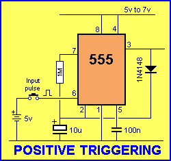
The only way to trigger a 555 with a positive
pulse is to have the output sitting HIGH. A positive pulse on pin 6 will
change the output to LOW. The voltage on pin 6 must be greater than 2/3 supply
voltage. When the 555 detects the trigger pulse, the output goes low and a
transistor inside the 555 takes pin 7 to the 0v rail. This starts to discharge
the 10u via the 1M resistor and when pin2 detects a LOW, the output goes HIGH
again. See Positive and negative triggering on
P1 of
this discussion.

555 PROJECTS
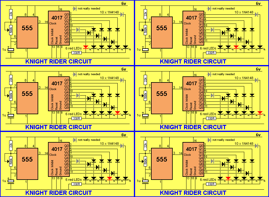
KNIGHT RIDER

In the Knight Rider circuit, the 555 is wired as an oscillator. It can be adjusted to give the
desired speed for the display. The output of the 555 is directly connected
to the input of a Johnson Counter (CD 4017). The input of the counter is
called the CLOCK line.
The 10 outputs Q0 to Q9 become active, one at a
time, on the rising edge of the waveform from the 555. Each output
can deliver about 20mA but a LED should not be connected to the output without
a current-limiting resistor (330R in the circuit above).
The first 6 outputs of the chip are connected directly to the 6 LEDs and
these "move" across the display. The next 4 outputs move the effect in
the opposite direction and the cycle repeats. The animation above shows
how the effect appears on the display.
Using six 3mm LEDs, the display can be placed in the front of a model car
to give a very realistic effect. The same outputs can be taken to driver
transistors to produce a larger version of the display.
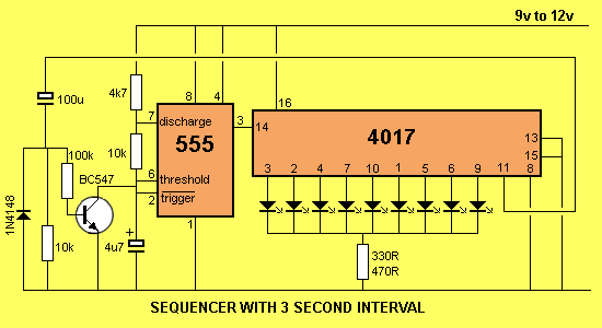
SEQUENCER WITH 3 SECOND HALT
The circuit runs 9 LEDs and the 10th output goes to the 555 via a transistor.
The 10th output takes the 100u HIGH and this turns on the BC547 to inhibit the
555 for approx 3 seconds.
The 100u gradually charges via the 10k and the voltage on the base of the BC547
drops to a point were the transistor turns off and the 555 oscillates 10 cycles
and halts again.
LIGHT DETECTOR

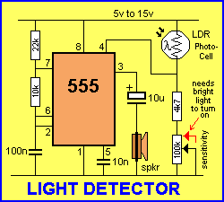
The Light Detector circuit detects light falling on the Photo-cell (Light
Dependent Resistor) to turn on the 555. Pin 4 must be held below 0.7v to turn
the 555 off. Any voltage above 0.7v will activate the circuit. The adjustable sensitivity
control is need to set the level at which the circuit is activated. When
the sensitivity pot is turned so that it has the lowest resistance (as shown in
red), a large amount of light must be detected by the LDR so that its
resistance is low. This produces a voltage-divider made up of the LDR and 4k7
resistor. As the resistance of the LDR decreases, the voltage across the 4k7
increases and the circuit is activated.
When the sensitivity control is taken to the 0v rail, its resistance increases
and this effectively adds resistance to the 4k7. The lower-part of the
voltage-divider now has a larger resistance and this is in series with the LDR.
Less light is needed on the LDR for it to raise the voltage on pin 4 to turn
the 555 on.
DARK DETECTOR

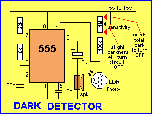
For the Dark Detector circuit above, when the level of
light on the photo-cell decreases, the 555 is activated. Photo-cells
(Photo-resistors) have a wide range of specifications. Some cells go down to
100R in full sunlight while others only go down to 1k. Some have a HIGH
resistance of between 1M and others are 10M in total darkness. For the circuit
above, the LOW resistance (the resistance in sunlight) is the critical
value.
More accurately, the value for a particular level of illumination, is the
critical. The sensitivity pot adjusts the level at which the circuit turns on
and allows almost any type of photo-cell to be used.
POLICE SIREN

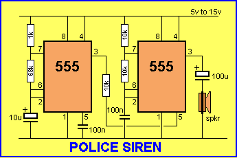
The Police Siren circuit uses two 555's to produce
and up-down wailing sound. The first 555 is wired as a low-frequency
oscillator to control the VOLTAGE CONTROL pin 5 of the second 555.
The voltage shift on pin 5 causes the frequency of the second oscillator to
rise and fall.
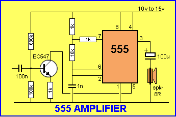
555 AMPLIFIER

The 555 can be used as an amplifier. It operates very
similar to pulse-width modulation. The component values cause the 555 to
oscillate at approx 66kHz and the speaker does not respond to this high
frequency. Instead it responds to the average CD value of the modulated
output. The output is low but demonstrates the concept of pulse-width modulation
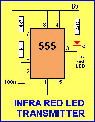
IR LED TRANSMITTER

The Infra-Red
Transmitter circuit produces a low for about 40uS and has a
duty-cycle of 90% HIGH and 10% LOW. It delivers a pulse of 150mA at a frequency
of about 2kHz to the infra-red LED.
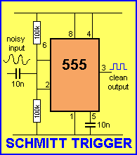
SCHMITT TRIGGER

A 555 can be
wired as a Schmitt Trigger to clean up noise signals.
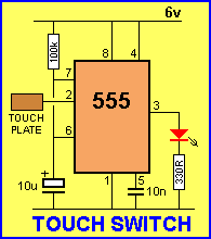
TOUCH
SWITCH

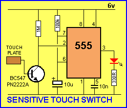
The Touch Switch circuit will detect stray voltages produced by
mains voltages and electrostatic build-up in a room. Pin 2 must see a LOW
for the circuit to activate. The circuit can be made 100 times more
sensitive by adding a transistor to the front-end as shown in the diagram
below:

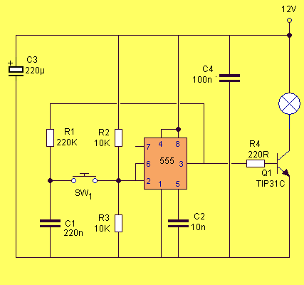
555 AS A FLIP FLOP
A 555 contains a flip flop
along with a couple of comparators.
When the output at pin 3 is 'high', C1 slowly charges through
R1 up to 12V; when it is 'low' C1 discharges through R1 down to 0V. Pressing
switch S1 upsets the 6v balance between R2 and R3 on pins 2 & 6 for a
split second, triggering the flip flop and changing the state of the output
from 'high' to 'low' or vice-versa. The wide hysteresis of the
555 (between 1/3 supply voltage and 2/3 supply voltage) limits false
switching from switch bounce.

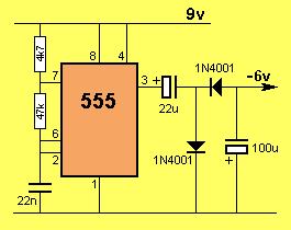
NEGATIVE
SUPPLY
A negative supply can
be generated with a 555 operating in astable mode. The generated voltage is
approximately 3v less than the rail voltage due to pin 3 rising to about
1.7v below rail voltage, plus the loss in the power diode. A small loss is
produced by the electrolytic in the diode-pump design, creating an overall
loss of approx 3v.
The output current should be kept to below 50mA, otherwise the output
voltage will drop further.

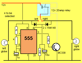
FLASHING
INDICATORS
This is a request from Daniel, one of
our subscribers.
He needs to flash "turn indicators" using a 555 and a single 20
amp relay. Here is our suggestion. The timing resistor needs to be
selected for the appropriate flash-rate.

Flashing the "TURN INDICATORS"
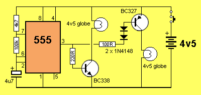
BICYCLE LIGHT
This circuit will alternately flash two 4.5v globes.

1.5v
LED FLASHER
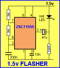
The 1.5v LED Flasher circuit will flash a LED at approx 1
flash per second. The ZSCT1555 IC from Zetex is designed to operate from a
single 1.5v cell and will continue to operate to a terminal voltage of 0.9v.
The circuit was originally presented by A J De-Guerin.
The first thing we note is the 1.5v supply voltage. From our previous
discussions we know that a LED will not illuminate until the voltage across
it reaches 1.7v. This means the circuit will not work unless the output is
generating a voltage higher than 1.7v.
And that is exactly what happens.
The circuit charges the 47u via the 330R resistor when the output of the
chip is HIGH. This puts a voltage of 1.5v on the electrolytic.
We will now replace the electrolytic by a 1.5v battery to make the
discussion easier to understand.
We have a 1.5v battery connected to the output of the chip with the positive
of the battery connected to the output of the chip.
When the output goes LOW, the left-hand-side of the battery falls by 1.5v
and this causes the right-hand-side to fall by the same amount.
The negative lead of the "battery" is actually 1.5v BELOW the 0v
rail and this puts a total of 3v (in theory) across the LED.
We have already learnt that the voltage across a LED will never rise above
1.7v (for a red LED) and so the voltage on the electrolytic creates a voltage
higher than 1.7v across the LED and the energy flows into the LED to make it
flash. The circuit is called a VOLTAGE DOUBLER.

I have just received a comment from a design engineer. He
has built a similar circuit to the one above and it has failed to
oscillate.
He comments:
I've even tried
different values for the components (lower values for the capacitor and
higher resistor values) with the same results. When I turn it on, the
output stays low and the voltage on the capacitor stays at around 1.1-1.2v
with a supply voltage of 1.5v. I've replaced the ZSCT1555 with another
one, with the same results.
With this type of uncertainty
about reliability, I would give this circuit a MISS! The
problem could be the low voltage. The circuit may work at a higher voltage
but this would negate its purpose. A 1.5v LED flasher
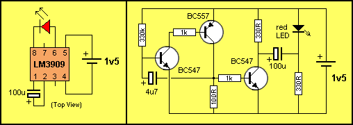
circuit can be created with a "3909" chip (LM 3909 - now obsolete, but you
may find one in a junk store) or by using the discrete 3-transistor
oscillator/driver circuit, shown below:

LM 3909 Flasher
circuit
3-Transistor Flasher circuit on 1.5v
supply
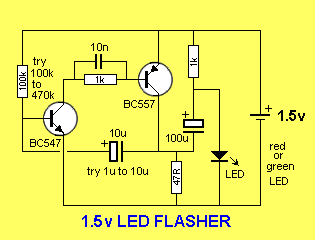
Here is another 1.5v flasher circuit
using 2 transistors:

SUMMARY
Hundreds of projects have been designed around the 555 and
its dual and quad versions.
Some of the projects will be presented in this e-magazine from time to
time but in general the consideration of the author is to design a circuit
with a chip that consumes less current. The 7555 meets this requirement
but has a very low drive capability.
The 555 (7555) is suitable for a circuit needing a single building-block
but if it requires more than one "block," it it suggested to go
to the 74c14 (Hex Schmitt Trigger IC) where 6 separate gates are available.
For an equivalent cost you get six times more value!
The versatility of the 74c14 Hex Schmitt Trigger will be covered in a future
issue.

