
Pages 22 to 41
Index
Pages:
1 to 21
Pages:
42 to 62
Pages:
63 to 85
.
The pages can be printed and collated into a book for easy reference.
More circuits and projects can be found on TALKING ELECTRONICS website:
http://www.talkingelectronics.com
Colin Mitchell
talking@tpg.com.au
Tel: 0417 329 788
|
CONTENTS |
|||
|
|
|
|
|
Page 22
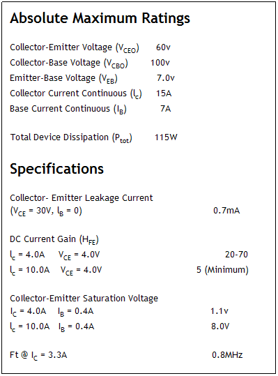
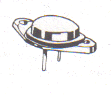
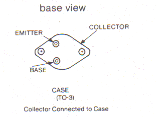
2N3055 Power Transistor
The 2N3055 is a medium speed
NPN Silicon Power Transistor designed for general purpose switching and
amplifier applications.
Features
•
DC current Gain (hFE) = 20-70 @ lc = 4.0A
•
Collector-Emitter Saturation Voltage = 1.0V @ lc = 4.0A
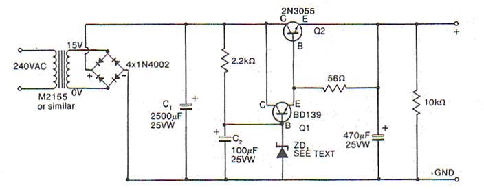
Low Ripple Regulated Power Supply
The excellent
characteristics of the 2N3055 at high currents (high hFE and
low collector-emitter saturation voltage) makes it ideal as a series
regulator transistor in regulated power supplies. The power supply
circuit shown below can be used when high current with low ripple is
required. Q, and Q2 form a high power Darlington. ZD1
and R1 provide a reference voltage at the base of Q1
The voltage output will be:- VOUT = Zener Voltage -
1.2v
Page 23
Car Voltage Converter for radios and cassettes
This circuit is suitable
for dropping a 12v car battery to the correct voltage to run portable
cassette players/radios etc. Using a 2N3055 might seem like a bit of an
overkill but they are cheap. The output voltage will be 0.7v lower than
the zener voltage, due to the voltage drop across the base-emitter
junction of the 2N3055. The 10 ohm series resistor stops excessive
current being drawn in the case of a short. The diode (1N4001) protects
the transistor in case of reverse voltage being applied.
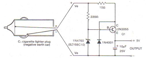
The output will drive transistor radios, cassette players etc. If the current drain is over 500mA, it is a good idea to put a heat sink on Q1. Mounting the converter in a metal box with Q1 on the lid (but insulated from it with a mica washer) will act as a good heatsink.
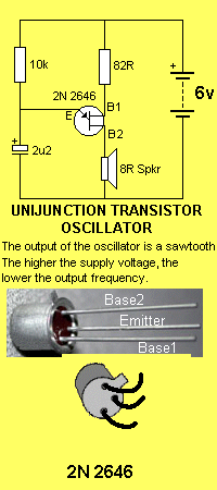
2N2646 Unijunction transistor
The 2N2646 is intended for
general and industrial triggering and oscillator circuits where circuit
economy is of primary importance. lt is a high speed switching device
with a low saturation voltage.
Absolute maximum ratings
Power Dissipation 300mW
RMS Emitter Current 50mA
Peak Emitter Current
(Capacitor discharge <10µF) 2A
Emitter Reverse Voltage 30V
Interbase Voltage
35V
Specifications
Intrinsic Standoff Ratio (VBB =
10v) ή 0.69
Interbase Resistance (VBB = 3v,
Ie = 0) RBB0
6.7
Emitter Saturation Voltage (VBB
= 10v, IE = 50mA) VE(sat)
2
Emitter Reverse Current (VB2E =
30V IB1 = 0) IE0 .001
Peak Point Emitter Current (VBB
= 25v) IP 0.8
Valley Point Current (VBB = 20v
RB2 = 100R) IV 5
Base-One Peak Pulse
Voltage V0B1
8.5
Basic Theory
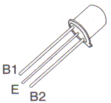
The unijunction transistor (UJT) has 3
terminals: Emitter (E). Base-one (B1 and Base-two (B2).
Between B, and B2 the UJT has a resistance of from 4.7k to
9.1k.
In operation the UJT emitter voltage VE is lower than the
emitter peak voltage VI. The emitter will be reverse biased
and only a small leakage current will flow. When VE equals VI
the emitter current will increase enormously. At the same time the
emitter-B1 resistance will fail to a very low level.
Page 24
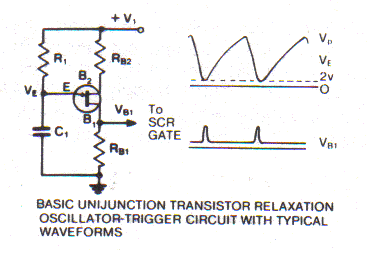
Basic UJT Pulse Trigger Circuit
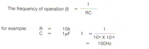
This is a basic relaxation oscillator. C charges through R, until the emitter reaches VP at which time the UJT turns on and discharges C1 via RB1. When the emitter has dropped to approximately 2v, the emitter stops conducting and the cycle starts again.
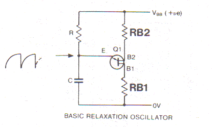
The design of the UJT trigger is very
broad.
RB1 is limited to values below
100 ohms for most applications. R1 should be a value between 3k and 3M. Supply
voltage can be from 10 to 35v. If the circuit is being used to trigger an
SCR, RB1 must be low enough to prevent DC voltage at the gate from
exceeding the maximum voltage that will not trigger the SCR. In practice,
keep RB, below 50 ohms.
The 2N2646 is specifically designed for
SCR trigger circuits. RB2 is typically 100 ohms.
Page 25
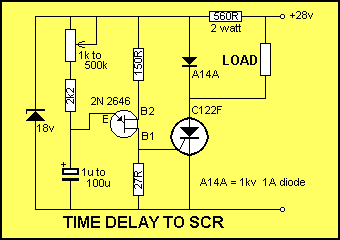
UJT/SCR Time Delay Relay
This circuit provides an efficient, high power and accurate time delay circuit. The SCR should be selected to suit the application. R5 and the zener diode maintain a stable supply for the UJT.
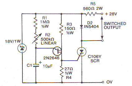
Initially the SCR is off. The timing
sequence is started by shorting out C1. C1 then charges through R1 and
R2 until the UJT triggers, developing a pulse across R4 which turns on
the SCR. Holding current for the SCR is supplied by current through R5
and D2. When the SCR triggers, it pulls the voltage across the UJT to <2
volts. This discharges C1.
The load this circuit will drive depends on the SCR used. A suitable
type would be a C106Y. This has a maximum current rating of 4A. This
would be enough to drive a relay (even one with a low coil resistance),
globes or an electric bell.
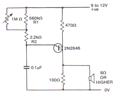
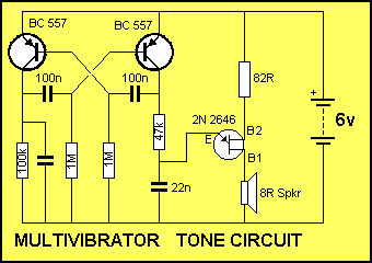
Metronome
This is the simplest
metronome circuit. It produces a 'click' similar to that of the
traditional mechanical device. The rate is variable from 40 to 220 beats
per minute. R1 sets the high rate limit and R2 the low rate limit.
Virtually any speaker is suitable. Supply voltage is from 12 to 18v.
While an 8 ohm speaker is suitable in this circuit, more volume and
higher efficiency can be obtained with a high impedance speaker, such as
a 40 ohm unit.
Page 26
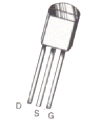
MPF102, 5, 6 Field Effect Transistors
The MPF102-6 series are
N-channel Junction-type field effect transistors.
The FET is a three
terminal semiconductor device. Input voltage is applied to a GATE
terminal and controls the current flowing from SOURCE to DRAIN
terminals.
An important feature of
the FET is its very high input impedance. Since the FET makes use of a
small input voltage to control a large output current, its gain is
specified in terms of TRANSCONDUCTANCE. Transconductance (gfs)
is equal to the change in drain current (dI0) divided by the
change in gate voltage (dVG) and the formula is usually
written as follows:-
gfs = 100Q(dlD/dVG)
where:
gfs is the
transconductance in micromhos
ID is the
drain current in DC mA
VG is the
gate/source voltage in DC volts.
Definitions of specifications
VGS (Gate/Source Voltage)
This is the maximum
voltage which may appear between gate and source. IDSS (Drain
current at zero gale voltage)
This is the current which
will flow in the drain/source circuit when VGS = 0. It is
given for specific drain/source voltages.
BVGSS
(Gate/Source breakdown voltage).
The voltage at which the
gate junction of a JFET will enter avalanche. Vp (Gate/Source
pinchoff voltage).
This is the
gate-to-source voltage at which the field just closes the conduction
channel. This is given for a specified value of VDS. The
value of the drain current is specified (usually 1µA).
|
FET Type |
BVGSS |
VP |
Idss |
gfs |
Ptot (mW) |
|
MPF102 |
25v @ IG 1µA |
0.5-8.0V @ VDS 15v |
2-20mA @ Vus 15v |
2,000-7,500 |
300mW |
|
|
|
|
|
|
|
|
MPF105 |
25v @ IG 1µA |
0.5-8.0V @ VDS 15v |
4-16 mA @ Vus 15v |
2,000-6,000 |
310mW |
|
|
|
|
|
|
|
|
MPF106 |
25v @ IG 1µA |
0.5V-4V @ VDS 15v |
4-10mA @ Vus 15v |
2,500-7,000 |
310mW |
All types are mounted in T092 plastic cases with pin connections as shown above.
Operation and Applications
The basic mode of operation of the FET amplifier is shown below. This is referred to as the common source amplifier. The gate to source circuit is the input and the drain to source circuit is the output.
When a moderate reverse or negative voltage is applied between gate and source, the gate junction becomes 'reverse biased' i.e. the voltage on the gate reduced the current flowing between the source and the drain. At a higher gate-source voltage, the drain-source current is cut to practically zero. This is referred to as the gate-source pinchoff voltage and is listed in the specifications as VP at a drain-source current of either 1 or 10uA. In practical circuits, the DC bias is developed across R2, due to the current being through it. This then puts the source at a positive potential relative to ground. The gate is at ground potential and therefore is at a negative potential relative to the source, R, sets the input impedance of the circuit since the gate of the FET draws virtually no current at all and so is seen by the load as a very high impedance.
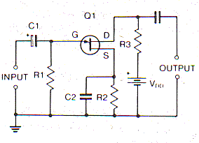
Page 27
*NOTE
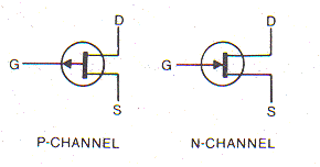
All the circuits and applications in these pages assumes the use of 'N-channel' Junction FETs, i.e. FETs in which the drain-source material is made of N-type silicon. However, these JFETs may be replaced in the circuits with P-channel JFETs if the polarity of the power supply is reversed.
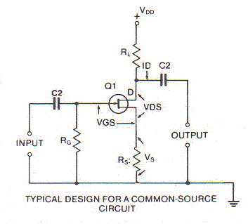
Typical Design for a Common-Source Circuit
When used as an amplifier, the FET is biased to a certain part of its response curve for lowest distortion and maximum available voltage swing. Assume that the FET has the following operating parameters
• VDs = 8V
(where VDs is the voltage between drain and source)
• ID = 0.5mA
(where ID is the drain current)
VGS = -2V
(where VGS is the gate-drain voltage or bias)
The power supply voltage is 22.5v
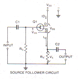
FET Applications Source Follower Circuit:
The source follower circuit is suitable where a high input impedance and low output impedance is required, but no voltage gain is needed. The figure below shows a typical source follower stage. Input impedance is set by the gate resistor RG. Output impedance is very low.
Page 28
RF Preselector
The uses for the FET are not limited to audio applications. The circuit below is for an RF preselector (a tuned amplifier) for the broadcast bands. The FET is a very good device to use in this application, due to its low cross modulation characteristics. Most cheaper receivers use ordinary bipolar transistors to keep costs down. The FET RF amplifier can also take higher signal levels without distortion. The preselector has a Volume Control style gain control between the FET and the emitter follower output stage. This means that only the FET has to handle high signal levels.
The tuning capacitor does not have to be exactly the same value as shown
in the circuit, any capacitor covering a similar range is suitable. The
aerial coil is wound on a 200mm length of ferrite rod. The main winding
consists of 42 turns of 22B&S enamelled wire. The second winding
consists of a further 6 turns. The preselector gives a marked
improvement on the reception of weak signals and aids in the attenuation
of adjacent channel interference and noise.

LDR Applications Light Beam Relay
In this circuit the LDR is held at a low resistance by light from a small globe. The circuit is actuated when the beam is broken. The resistance of the LDR then goes high. The circuit is set up so that with the light shining on the LDR the input voltages at the two input terminals of the 741 op amp hold its output 'low'. When the LDR goes to high resistance the op amp's output goes 'high'. This turns the transistor 'on' and pulls in the relay.

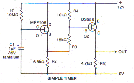
Simple timer
The very high impedance of the FET makes it suitable for a wide variety of timer circuits. The circuit below gives one such example. With C1 given a value of 1µF, it will give timing periods of 40 sec, and with a value of 100µF it gives a period of 35 minutes. The FET is wired as a source follower and has its gate taken to the junction of a time constant network R1-C1 When the supply is first connected, C1 is discharged, so Q1 gate is at ground potential, and the source is a volt or two higher. The base of Q1 is connected to the source of Q1 via R3, so Q2 is turned on and 12v is across R5, When the supply is connected, C1 starts to charge via R1, so the voltages on the gate of Q1 (and on the source) rise exponentially towards the 12v supply. When the voltage reaches approximately 10.5v the bias on Q1 falls to zero and Q2 switches off, the voltage across R5 falls to zero.
Page 29
FET Voltmeter
The very high input impedance of the FET makes it the ideal basis of a voltmeter. The circuit below has a basic sensitivity of 22M ohms per volt. Maximum full scale sensitivity is 0.5V, and input sensitivity is a constant 11.1 M ohms on all ranges. R7,R8 R9 form a potential divider across the 12v supply. R8 is adjusted for a zero meter deflection. Any potential across the gate circuit of Q1 causes the circuit to 'unbalance'. To avoid drift, the power supply should be stabilized if possible.

555 Light Switch
The use of the 555 timer
1C with an LDR provides a high performance light switch.
An LDR is a Light Dependent Resistor and is a very low cost way of
detecting light.
The 555 is used with its trigger and thresholds tied together to provide
a Schmitt trigger with a very low input current but which can drive a
relay taking up to 200mA of current. The trigger is activated when the
light level on the LDR falls below a predetermined level. The relay
energizes when the voltage on pins 2 and 6 is greater than 2/3Vcc.
It de-energizes when the voltage falls below 1/3VCC.
This gives a hysteresis of 1/3VCC.
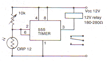
The 555 can supply current up to 200mA, so the relay type is not critical. Any with a coil resistance from 100-280 ohms would be suitable.
Page 30
Light Sensitive Switch
This circuit makes use of the wide change of resistance of the LDR. Between positive and negative supply there is a voltage divider. The bottom section is a variable resistor RV1. The top half is formed by the LDR and a 4.7K ohm resistor in series. In low light conditions when the resistance of the LDR is very high, the bias to the Darlington pair formed by TR1 and TR2 is very low, and they do not conduct. When the light level rises, the resistance of the LDR falls. This turns the transistors 'on' and pulls in the relay.
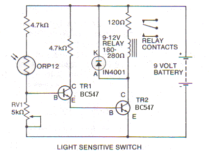
The LDR should be an ORP12 or similar. The relay should have a pull in voltage of 9V or lower and a coil resistance of 280 ohms or higher.
Photo Electric Relay
This circuit is basically a bistable multivibrator. When the light level is low and the resistance of the ORP12 is high, transistor Q1 conducts and Q2 is off. As the level of illumination increases the resistance drops until Q1 cuts off and Q2 turns on, energizing the relay coil.

The relay should have a coil resistance of 180 ohms or higher and a pull in voltage of 9V or lower
Page 31
LEDs

Features
• Low power consumption
• IC compatible
• Long life
Absolute Maximum Ratings
|
|
Red |
Green |
Yellow |
Amber |
Orange |
|
Reverse Voltage |
5v |
5v |
5v |
5v |
5v |
|
Av forward Current |
20mA |
30mA |
30mA |
30mA |
30mA |
|
Peak Forward Current |
200mA |
200mA |
200mA |
200mA |
200mA |
|
Power Dissipation |
100mW |
100mW |
100mW |
100mW |
100mW |
Page 32
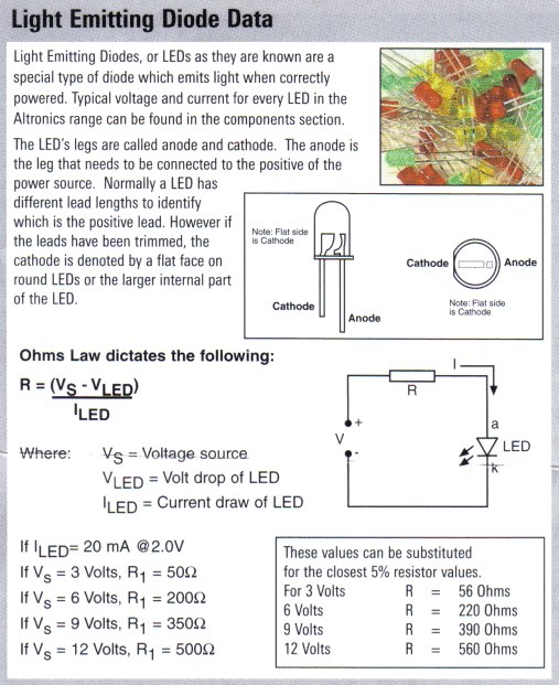
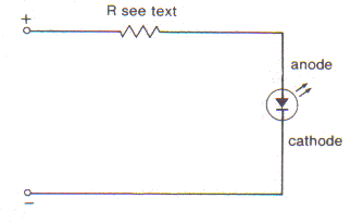
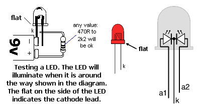
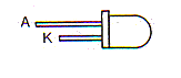
LED Basics

LEDs are used in the
'forward biased' mode. i.e. positive on the anode and negative on the
cathode. This voltage drop is stated in the specifications (eg 1.7V for
a red LED), If the LED is used on a higher voltage than this, a current
limiting resistor must be used.
The following formula can
be used:-
R = (E -1.7) x 1000/I
R is the resistance in
ohms. E is the DC supply voltage. I is the LED current in milliamps.
A common LED current is 20mA.
Some calculated values are:-
For 6v use 220 ohm.
For 9v use 390 ohm.
For 12v use 560 ohm.
For 24v use 1.2k ohm.
If a LED is reverse biased, it will break down, in a similar way to a zener diode. This occurs at 3-5V. It usually damages the diode if a high current flows.
Operating LEDs from the mains
This circuit uses a capacitor as a voltage dropping element. A 1N4148 diode is placed across the LED for rectification. As the voltage across the LED is negligible compared with the supply, capacitor current is almost exactly equal to mains voltage divided by the capacitor reactance. At 50Hz, a 0.47µF will result in a LED current of about 16mA. Resistor Rs limits current on transients. A value of 270 ohms is adequate.

Page 33
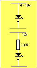
The Flashing LED
The Flashing LED has a chip inside the device to produce the
flash-rate. Simply connect the LED to a supply voltage (4v to 10v) and
the LED will flash at a rate of approx 2Hz. No external resistor is
needed up to 10v. For voltages higher than 10v, the resistor should be
100 ohms for each volt above 10v.
This is the only “LED” that does not need a resistor when connected to a
supply as it has an internal resistor. All other LEDs MUST have a
resistor in series to limit the current and prevent damage.
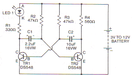
LED Flasher
This circuit for a LED
flasher is very simple and cheap to make and will work on any voltage
between 3v and 12v. As the voltage is raised the value of R1 must be
increased - The speed can be changed by altering the value of C1
and C2 and/or R2 or R3. Raising the
value of C1 and C2 slows the rate down.
Raising the value of R2 and R3 also slows it down.
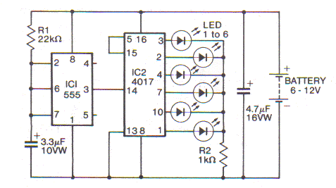
LED Chaser
This circuit acts as a
LED chaser. The 4017 is driven by a 555 working as a free-running
multivibrator. The speed can be changed by altering C1 or R1.
Page 34
CQY89 Light Emitting
Diode - Infrared LED
The CQY89 is an infrared LED, similar in performance to
conventional LEDs, but emitting light in the infrared region. This is
visible to the human eye. Unlike conventional LEDs, infrared LEDs are
usually pulsed rather than fed with continuous DC. They find wide use in
alarms and in remote control equipment.
Specifications
Maximum Forward
Current 130mA
Maximum Reverse
Voltage 5V
Maximum Power
Dissipation 215mW
Maximum Forward
Current 130mA
Beamwidth between half
intensity directions (IF = 100mA] 40° typ.
Wavelength at peak
emission (lr = 100mA) (λpk)
930nm typ.
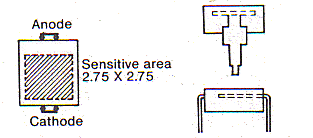
BPW34 photosensitive diode
This device is mainly used in combination with a light source
for go/no go detection as in card readers and industrial safety devices.
Specifications
VR Forward
voltage 32V
Total power
dissipation 150mW
Spectral sensitivity (VR
=5V) 70nA/lx
Dark Reverse Current (VR=10;
Ee=0) 2nA
Light Reverse Current
(VR = 5; Ee=
1mW/cm2;λ = 930nm) 10µA
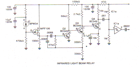
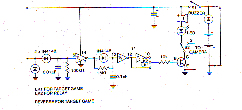
BPW34/CQY89 Infrared light-beam relay
Receiver
The light is picked up by
the photodiode a BPW34. It is wired so that a current is generated that
is proportional to the light falling on it. The FET acts as a source
follower and impedance matches to the next stage. The amplifier after
this acts as a bandpass filter. Its output is coupled to a CMOS Schmitt
trigger, followed by a rectifying circuit and a pulse stretcher. This
drives a transistor and a buzzer and LED.
Page 35
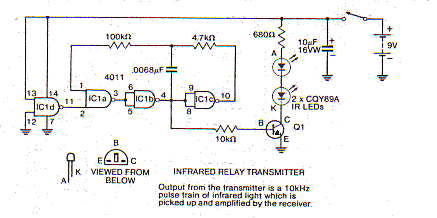
Transmitter
A CMOS oscillator drives an output stage consisting of a BC547 transistor and two CQY89 infrared LEDs. Current drive is limited by the 680 ohm resistor. If greater range is required, this resistor may be reduced to a minimum of 150 ohms with a consequent increase in current consumption.
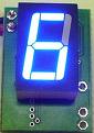
7 Segment LED Displays
The 7 segment display is found in many displays such as
microwaves, lifts, ovens etc. It consists of 7 LEDs that have been
combined into one case to make a convenient device for displaying
numbers and some letters. There are basically two different size
displays. 0.3” and 0.5”. The two sizes are shown below:
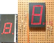
0.3" and 0.5"displays
Displays come is a range of colours and brightness levels.
Most come in super-bright and these are preferred so the display can be
seen during the day. They are not much more expensive but give a much
better illumination.
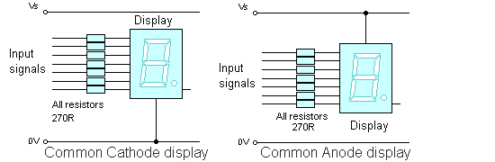
All displays also come in COMMON CATHODE and COMMON ANODE.
The COMMON CATHODE display has all the cathodes of the LEDs tied
together and connects to the pin that goes to the 0v rail. This is the
most common type of display.
Page 36
The Common Cathode and Common Anode displays are wired as shown below:

The project above from
JJM turns on each segment of the display to show how each letter and
number is produced. The second photo is a white 7-segment display.
Electronic Die
This circuit consists of three sections: an oscillator, a counter, and the display. The oscillator uses three sections of a 4069 hex inverter. The 4029 is a four bit counter with the capacity to count from zero to 15. The 4511 driver/decoder takes binary output and decodes it to drive a seven segment display. The current to the 7-segmenl display is limited by seven 560 ohm resistors. The display is a common cathode type, and any 7-segment display can be used.

Page 37
Counter
This circuit uses a 7-segment display as the output of a basic counter circuit. The 7490 counts decimal pulses and converts them to a BCD code. Its output is fed to a 7475 latch. This stores the outputs from the decade counter. The four binary outputs are taken from the 7475 to a 7447 LCD to the 7 segment LED decoder, which drives the display.

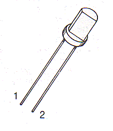
THE UNIJUNCTION TRANSISTOR
|
|
|
Page 38
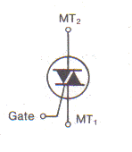
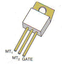
SC151D TRIAC
The SC151 D
is a medium power plastic package TRIAC designed for economical mains
power and lighting control. Unlike SCRs, the SCI 51 D is a bidirectional
thyristor - when triggered, it conducts in both directions and can be
triggered by a positive or negative gate signal. TRIAC (Triode AC
Semiconductor). The diagram below shows the V/l characteristics of the
Triac. A gate current of the specified level of either polarity will
trigger the triac into conduction in either quadrant, provided the
applied voltage is less than VB0.
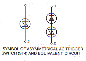
Triggering may be from DC, rectified AC or pulse sources such as unijunctions, neon lamps or breakdown devices such as the ST4.
Specifications
Voltage
Rating
400V
Current
Rating
15A RMS
ITSM Maximum
peak one cycle non rep. surge current 110A
IDRM Blocking
Current at 25°C
0.1mA max
dv/dt Off State, Tc
= 100°C, Rated VDRM, gate O/C 250V/µS
(typ.)
FIRING
IGT Max DC
Gate Trigger current VD=12v, 25°C
50mA
VGT Max Gate
Trigger voltage VD= 12v 25°C
2.5V
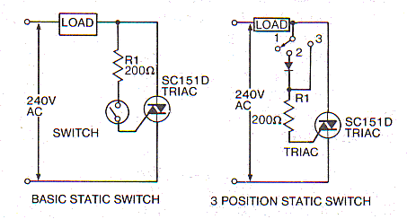
Triac as a switch
This gives improved performance over a conventional switch, as there can be no arcing or contact bounce. This circuit shows a simple three position power control. In position one there is no gate connection, so power is off. In position two there is gate current during one half cycle only and load power is half wave. In position three the gate is triggered on both half cycles and the power is full on. For a simple on-off switch, just delete the diode.
Because the contacts only carry current for the few microseconds needed to trigger the triac, the actual switch can be almost any small device: reed relays, thermostats, pressure switches or program/timer switches.
Page 39
Lamp dimmer/Heater controller
R1 and C1 are a phase shift network - they produce a variable delay in the waveform applied to the ST4 and hence the triac. When the voltage across C1 reaches the breakdown voltage for the ST4, C1 partially discharges into the triac gate through the ST4. This pulse triggers the triac into conduction for the remainder of the half cycle.
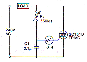
This easy-to-build controller is ideal for dimming lights, and controlling the output of electric heating type appliances. The light or heater element etc is placed where the 'LOAD' is marked on the circuit.
ST4 Asymmetrical AC Trigger Switch
The ST4 is an integrated
triac trigger circuit that provides wide range hysteresis-free control
of voltage.
It behaves like a zener
diode in series with a silicon bilateral switch (a symmetrical device).
The zener provides
asymmetry since the switching voltage is increased in one direction by
the zener breakdown voltage.
Switching voltage:
VS1
14v-18v
VS2
7-9v
Switching current
I S1 I
S2 80µA
On-state voltages
VF1 (I =
100mA) 7-10v
VF2 (I =
100mA) 1.6v max
Peak pulse voltage
V0
3.5v min
Page 40
C122D/C122E Silicon Control Rectifier
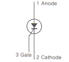
The C122Dand 122E are medium power plastic package SCRs designed chiefly for mains power and motor control. The SCR is a unidirectional device, (current flows through it in one direction, from anode to cathode).
The SCR is a three terminal semiconductor device. The three terminals are the anode (A), cathode (K). and the gate (G). With no voltage applied to the gate terminal, if a voltage is applied to the SCR anode and cathode terminals, (anode positive with respect to cathode) current flow is prohibited. If the supply is reversed the flow is likewise prohibited. Thus with no signal applied, the SCR appears as an open circuit as long as its diode junctions do not break down. The SCR is brought into conduction by applying a current into the gate terminal. This will cause it to conduct in the forward direction (i.e. with the anode positive and the cathode negative). The gate voltages required vary from approximately 1.5- 6.0v. Once the SCR is turned on the gate no longer controls the circuit and the SCR only drops out of conduction when the anode-cathode voltage falls to near zero. At this instant, the current through the device falls to zero.
Specifications
C122E
Vdrm (Repetitive off state
voltage. Max between anode and cathode) 500V
It (RMS Current through
SCR)
8 Amps
IGT (Peak
Positive gate current) (Tc = 25°C)
25mA
VGT (Peak
Positive gate voltage) (Tc =
25°C) 1.5V
Pg (AV) (Max Gate
power)
0.5W
IH Holding Current (Current below which the SCR will drop out
of conduction) (Tc
= 25°C) 30mA
dv/dt Rate of change of
on-state voltage (Max. rate of change of
anode-cathode voltage which will not turn SCR on)
50V/µsec(typ.)
The C122D differs only in
that its VDRM is only 400v as against 500v for the C122E.
The SCRs listed above are medium power SCRs (Silicon Controlled Rectifiers) designed primarily for economical mains power and motor control. They are three terminal devices (see above). The electrodes are anode, cathode and control gate. They are unidirectional devices i.e when triggered 'on' they only conduct in one direction. The SCR is a 'regenerative' device. It is triggered 'on' by injecting a signal into the gate. As noted earlier, once the gate has triggered the SCR 'on' it no longer controls the gate. The only way to cause the SCR to stop conducting from cathode to anode is to drop the anode cathode voltage to a level where the current flowing from anode to cathode is below the 'holding level'. This is indicated in the figure above. In practice, this is not a problem, since SCRs are normally used to control fluctuating voltages such as the AC mains. The 'drop out' of the SCR occurs as the mains voltage goes through zero.
Page 41
Applications
SCRs are current rather than voltage triggered devices. This means that they must be fed from a relatively low impedance source i.e. one in which the voltage won't drop down under load from the gate. In a way analogous to a relay or a solenoid, the SCR requires certain minimum anode current if it is to remain in the 'closed' or conducting state. If the anode current drops below the minimum level, the SCR reverts to the forward blocking or 'open' state. The following circuit shows a basic R-C-Diode trigger circuit giving full half wave control. On positive half cycles the capacitor C will charge to the trigger point, at a speed determined by the time constant of R and C. On the negative half cycle, the capacitor is reset by CR2, resetting it for tire next charging cycle, Thus the triggering current is supplied by the line voltage.
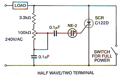
C122D, C122E, C106D SCRs Phase Control Circuit
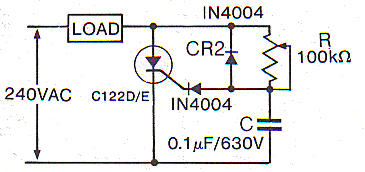
Improved phase control circuit
The following diagram shows a circuit using a neon lamp as a breakdown device. This gives smoother control and improved performance. The neon triggers when the voltage across the two 0.1µ capacitors reaches the breakdown voltage of the lamp (60-90V). Control extends from 95% to full off.
The neon lamp phase controlled circuit shown below combines the low cost of the simple RC circuit shown before but gives improved performance. The circuit below gives half wave control from 95% on to full off. Full power can be easily obtained by putting a switch across the SCR. The circuit uses a neon. This gives the following improvements:
A higher impedance circuit can be used for control.
As a result, the control element (which
is a 100k pot in the circuit below) can be replaced by a high impedance
device such as a thermistor or light dependent resistor, for heating or
light control applications.
.
This
completes Pages 22 to 41 of Data Book 1
http://www.talkingelectronics.com
Sept 2008 Nothing is copyright. You can copy anything
Colin Mitchell
to pages: 42 to 62