|
Pages 42 to 62
Index
|
||||||||

Page 42
OP-AMP Basics
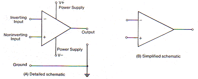
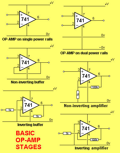
The op-amp is a very high gain DC amplifier. This is quoted in specifications as typically in the range of 20,000 to 100,000 times. The symbol for the op-amp is shown below. As can be seen, there are two inputs, the inverting and the non-inverting. If a signal is applied to the -input (inverting) with the + input (non-inverting) grounded, the polarity of the output signal will be opposite that of the input. If the signal is applied to the + input with the - input grounded, the polarity of the output signal will be the same as the input signal. For an AC signal, this means that when it is applied to the - input, the output signal will be 180° out of phase with the input. If the same signal is applied to both the + and - inputs, the two signals will cancel each other out. The op-amp responds to the difference between its two inputs - hence the name differential amplifier. The ability of an op-amp to cancel two equal signals at its pins is referred to as its common-mode rejection.
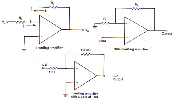
The most common op-amp circuit is shown
below and uses two external components;
1) an input component, R1
2) a feedback component, RF.
When the feedback component is between the op-amp output and the
negative input the op-amp is said to have negative feedback. When the
feedback component is between the op-amp output and the positive input,
the circuit is said to have positive feedback.
With no feedback applied, the gain is set by the op-amp itself and is very high (at very low frequencies). This is referred to as the open loop gain. When negative feedback is applied, the gain is specified by the feedback components, and is referred to as the 'closed loop gain'.
Gain = Rf / Ri
Thus to produce an amplifier with a
gain of 100, we can use an input resistor of 1k and a feedback resistor
of 100k. This is shown below with the op-amp connected as an inverting
amplifier. To produce a non-inverting amplifier, the signal is applied
to the non-inverting input and the feedback components are left on the
non-inverting side. This is shown following.
Page 43
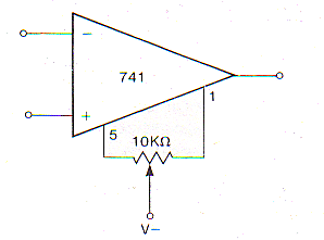
Output Offset
The steady state output of an op-amp with negative feedback is zero when the input is zero. The actual DC output (in a real op-amp) is usually not quite zero, and this small unwanted signal is usually referred to as the output offset voltage. Most op-amps have means of nulling this out. Fig A shows the most common method, where the op-amp has special nulling pins. If these are not available, the method in Fig B can be used.

Frequency Compensation
Circuits using op-amps must be designed so that the open loop gain of the op-amp itself is greater than the closed loop gain of the circuit for all frequencies of operation. The gain drops as the frequency increases. This is mainly due to the large amounts of internal 'compensation' used to make sure that they do not oscillate. Frequency compensation is the shaping of the frequency responses of the op-amp so that it does not oscillate due to internal phase shift. This phase shift acts as a time delay. When this delay is great enough so that the input signal is delayed 360° (a complete cycle), the amplifier will oscillate. This is because the 'negative feedback' signal, instead of being in opposition to the input signal will actually reinforce it. Thus the input signal keeps getting bigger and bigger - positive feedback occurs. To make sure this can't happen, the open loop gain of the amplifier is shaped either internally (eg. internal compensation in the 741 op-amp) or externally so that at the frequency where the phase shift approaches 360°, the gain is less than unity.
In practice we need to be careful that we don't design a circuit which sets a closed loop gain higher than the op-amp can 'keep up with' at high frequencies. For example, the 741 op-amp has a unity gain bandwidth of 1MHz (i.e. at 1MHz its gain is x1) and its gain rolls off from approximately DC at a rate of x10 per decade. This means that at 100Hz it will typically have a gain of 10,000 times, but at 1000Hz this has dropped to 1000 times. By 10,000Hz it has dropped to 100 times. By 100kHz it has dropped to only 10 times.
Power Supply Rejection Ratio
This is the ratio of change in input voltage to the change in supply voltage. This is the ability of an op-amp to reject power-supply-induced noise, hum and drift. Voltage changes on the supply lines are coupled into the amplifier and appear as part of the input signal. Because of this, the power supply hum and noise at the output will be amplified by the gain of the op-amp. Thus if the op-amp is being used as a unity gain inverter, the hum and noise at the output will be that at the input. If the gain is set high, then it will be amplified accordingly. The figures presented for power supply rejection in the data are for unity gain and will deteriorate in direct proportion to the gain of the op-amp. To give an example:-
If an op-amp has a power supply reaction of 80dB (10,000) times, then a power supply hum level of 1v will only produce a hum level of 0.1mV at the output. However, if the op-amp is used at a gain of 1,000 times, this hum will be amplified 1,000 times as well, producing 0.1v of hum in the output signal. Also, power supply rejection will usually deteriorate at high frequencies.
Latch-up
Latch-up is the 'sticking' or 'locking-up' of the output of an op-amp when the maximum differential input voltage is exceeded. In the latch-up condition, the output is stuck at either the positive or negative maximum output voltage, and the input is ineffective in affecting the output. Most of the modern op-amps such as the 741 have eliminated this problem.
Page 44
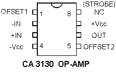
CMOS Operational amplifiers
The CA3130 is a CMOS output operational amplifier, originally
designed by RCA. It is a good choice when you want the full output
voltage swing to go from rail to rail.
Like the conventional
op-amp, the 3130 has an inverting and a non-inverting input. These go to
a pair
of p-channel MOSFETs set up as a differential amplifier.
Compensation is applied between pins 1 and 8. Compared to the 741, the 3130 has about the same open loop gain and input offset voltage.
The input impedance is about a million times higher (2x10¹² ohms rather than 2x10⁶) and the input bias and offset currents are proportionately lower. Slew rate is about 20 times better, at 10V/µsec. The output of the 3130 is sensitive to capacitive loading. It works on voltages as low as 5v but will only work up to 16v total. Another similar device is the CA3140. It has a bipolar output stage and will work up to a full ±15V. Frequency compensation is internally provided. The output easily drives capacitive loads. It has the same high slew rate and input impedance of the 3130
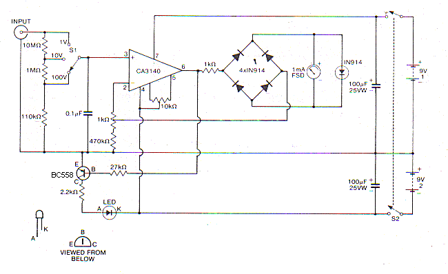
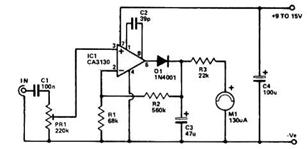
CA3140 High Impedance DC Voltmeter
This circuit makes use of the very high impedance of the CA3140 to produce a high performance DC voltmeter with an input impedance of 11M ohms. The instrument uses a cheap 1mA FSD movement and has a diode bridge to correct polarity. If reverse polarity is applied to the instrument, the op-amp biases the BC558 'on' and this turns a LED on.
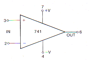
741 Operational
Amplifier
The 741 is a high performance operational amplifier with high
open loop gain, internal compensation, high common mode range and
exceptional temperature stability. It is short circuit proof and allows
for nulling of offset voltage.
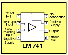
Features
• Internal frequency compensation
• Short circuit protection
• Offset voltage null capability
• Excellent temperature stability
• Hign input voltage range
• No latch up

Absolute Maximum Ratings
Supply Voltage ±18v
Internal Power Dissipation 500mW
Differential Input
Voltage ±30v
Input Voltage (either input) ± 15v
Output Short Circuit Duration Indefinite
Page 45
Applications
The 741 is an internally compensated op-amp for unconditional stability. Its gain falls off at 6dB per octave/ 20dB per decade above DC. i.e. as the frequency doubles, the open loop gain halves.
It has a unity gain bandwidth of 1MHz i.e. at 1MHz its gain has dropped to x1.
Offset Adjustment


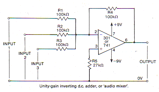
Audio Mixer

Difference Amplifier
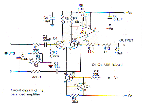
The circuit below shows a typical
application for a unity gain difference amplifier- a balanced input
audio amplifier. The output is the difference between the two input
signals. These circuits are often used in audio when long leads must be
run - say between a microphone and an audio mixer. Signals such as hum
or buzz from lighting controllers (triac dimmers are renowned for their
electrical 'noise' producing ability!) are picked up along the cable.
The difference amplifier gets this signal equally on both inputs and
cancels it out. The good 'wanted' signal will be seen as a difference at
the input terminals and will be passed through.
Page 47
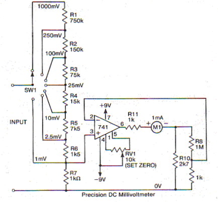
Precision DC Millivoltmeter
The very high DC performance of the 741 and 301 make them ideal for DC measuring equipment. The circuit following is for a precision DC millivoltmeter. It will give full scale voltage readings from 1mV to 100mV in seven ranges.
Peak
reading VU Meter

Page 48
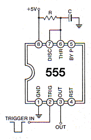
555 Timer
The 555 is a highly stable device designed for generating accurate time delays or oscillations. Additional terminals are provided ' for triggering or resetting. In the time delay mode (monostable mode) the time is set by one external resistor and one capacitor. In the astable (free running) mode the frequency and duty cycle are set by two external resistors and one capacitor. The circuit can be both triggered and reset on falling waveforms. The output circuit can source or sink up to 200mA. TTL circuitry can be driven directly from the output.
A dual version of this IC
is available, the 556.
Features
555 Timer IC
• Timing from microseconds to hours
• Adjustable duty cycle
• Sink & source 200mA
• 4-15V operation
• Temperature stability >0.005% per°C
Absolute maximum ratings
Supply +18V
Power
dissipation 600mW

Specifications
Timing Error, monostable Temperature drift 50ppm/°C
Supply Drift 0.1 %/V
Timing Error, astable
Temperature Drift 150ppm/°C
Supply Drift
0.30%/V
Trigger Voltage
Vcc 15V (Itrig = 0.5µA) 5V
Vcc 5V 1.67v
Control Voltage
VCC15V 10v
VCC 5V 3.3v
555 Modes & uses
Free-running: astable multivibrator
When powered from a 5v supply the 555 is directly compatible with TTL. It can also run from 4-15v and can source and sink several hundred milliamps at its output.
One end of the timing capacitor is connected to ground, the other to the positive supply via resistor(s) allowing the use of electrolytics.
The high input impedance allows the use of large resistors and small capacitors. Up to 1000:1 frequency range can be obtained from a single capacitor by changing the resistance timing element.
Astable operation
1. Output (pin 3) is high
2. Charge on capacitor is low
3. Discharge transistor not conducting
4. Capacitor starts to charge
5. When voltage across the capacitor reaches two-thirds of the supply voltage the comparator triggers. Output goes low, capacitor is discharged via R2. When the voltage on the capacitor drops to one third of the supply the comparator flips the circuit back. Then the whole sequence repeats for the next cycle.
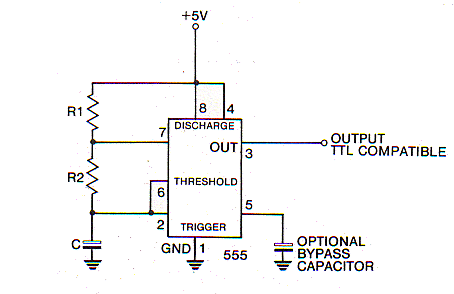
If R2 is made large compared to R1, output is low but symmetry of waveform is high.
Page 49
Altering the Duty
Cycle
The duty cycle is the 'on' time as a percentage of total
cycle time. This is normally limited to 50%. By adding a diode, a duty
cycle of less than 50% can be achieved.
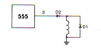
Curing Latch-up problems
Latch-up when driving an inductive load can be avoided by adding two diodes as shown in the circuit below. This stops negative voltage from reaching pin three.
Fine Control of Timing/Frequency
Pin 5, the control pin, is primarily used for filtering when the device is used in noisy electrical environments. However, by putting a voltage on this point, it is possible to vary the timing of the device independently of the 'RC' components. This control voltage may be varied from 45% to 90% of supply voltage in the monostable mode and from 1.7V to Vcc (supply voltage) in the astable mode.
Monostable operation
1. Bringing trigger from +V to ground starts sequence.
2. Output goes positive.
3. Clamp is removed from timing capacitor which then charges to two thirds of supply voltage. The threshold comparator then flips the circuit over. Output goes to ground and the capacitor is rapidly discharged to ground.
Page 50
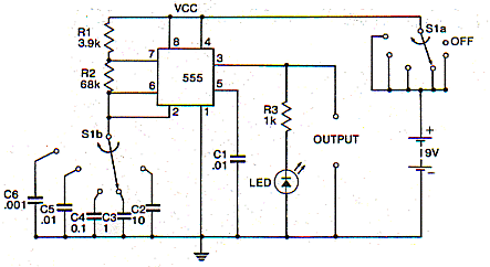
Square Wave
Oscillator
This simple circuit provides square waves at five switched
frequencies from 1Hz to 10kHz. It uses the 555 in the astable mode.
Timer circuit
This circuit produces a warning tone after a preset period. The delay period is controlled by C1/R1 and RV1 and can be adjusted from a few milliseconds to approximately 500 seconds. The 555 is normally "switched off". C1 discharges via R1 and RV1. When it has discharged, the 555 is turned 'on' via Q1 and oscillates, producing a warning tone.

Special Version of
the 555
ICM7555
The ICM 7555 is a CMOS timer IC providing significantly improved performance over the standard 555 timer. At the same time it will act as a direct replacement for this device in most applications. Improved parameters include the low supply current, wide operating supply voltage range, low threshold, trigger and reset currents, no crowbarring of the supply current during any output transition, higher frequency performance and no requirement to decouple the control voltage for stable operation. A dual version of the 7555 is available, the 7556, with two timers sharing only V+(VCC) and V-(GND). They are both capable of sourcing and sinking sufficient current to drive TTL loads and have small enough offset to drive CMOS loads.
Features
• Low supply current (80µA typ)
• Ultra low trigger threshold. (20pA typ)
• High speed operation (500kHz guaranteed)
• Wide supply range 2v to 18v
• No crowbarring of supply during reset.
• Can be used with higher impedance timing elements than 555.
• Complete static protection.
Page 51

Absolute Maximum Ratings
Supply Voltage
+18v
Input Voltage
Trigger Supply + 0.3V
Threshold Supply - 0.3V
Reset control voltage
Output Current 100mA
Power Dissipation 200mW
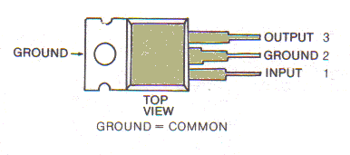
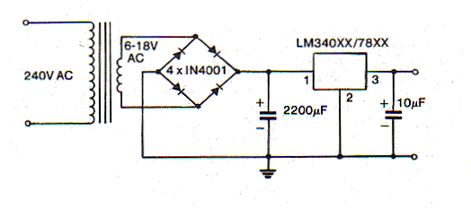
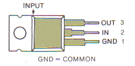
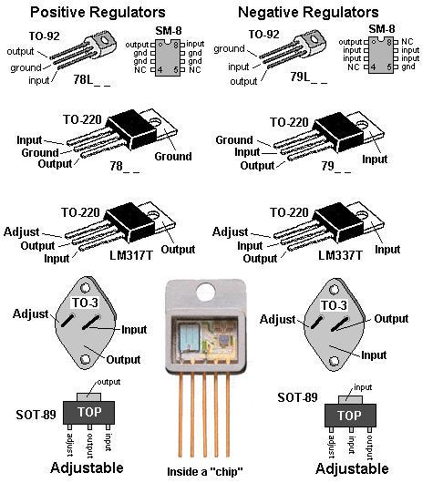
LM340 and
78XX series 3 terminal regulators LM340T5, 12, 15 7805,
7812, 7815
The LM340 series of positive 3 terminal regulators offer
similar performance to the 78XX series. They are complete voltage
regulators with outstanding ripple rejection and superior line load
regulation.
Current limiting is included to limit peak output current to a safe level. Safe area protection for the output transistor is provided. If internal power dissipation is too high, thermal shutdown occurs. Although designed primarily as fixed voltage regulators, these devices can be used with external components to obtain adjustable voltages and currents.
Features
• Maximum 1A output
• Output voltage tolerance ±2%
• Load regulation 0.3%
• Thermal overload protection
• Short circuit current limit
• Output transistor safe area protected
• Continuous dissipation 15W
Basic use as a fixed regulator
The 10µF capacitor across the output is needed for stability and improves the transient response of the supply.
Page 52
Specifications @ 25°C
|
|
µA7805/ LM340T-5 |
µA7812/ LM340T-12 |
µA7815/ LM340T-15 |
|
Output voltage |
5v ± .25 |
12v ± .6 |
15V ±.6 |
|
Ripple rejection |
80dB |
72dB |
70dB |
|
Input voltage (minimum to maintain line regulation) |
7.3v |
14.5v |
17.5v |
|
Dropout voltage |
2.0 |
2.0 |
2.0 |
|
Peak output current |
2.2A |
2.2A |
2.2A |
|
Short circuit current |
2.1A max |
1.5A max. |
1.2A max. |
|
Load regulation (5mA to 1.5A) |
12mV typ. |
12mV typ. |
12mV typ. |
|
Bias current |
8mA max |
8mA max |
8mA max |
|
Absolute max input voltage |
35v |
35v |
35v |
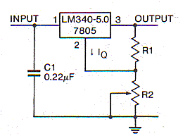
Applications
Apart from the normal use as a fixed voltage regulator, the LM340/78XX can be used in a variety of ways with the addition of external circuitry.
Adjustable output
This simple circuit gives the LM340T-5 variable output voltage according to the formula:
Vout = 5v + (5v/R1+IQ)R2
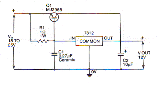
Boosting the current output of the LM340T/ 78XX series
This circuit supplies regulated outputs at up to 5A. At low currents Q1 is off. Only above 600mA is it biased on.
Page 53
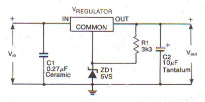
Providing fixed higher voltages
The output voltage of the LM340T/78XX series can be increased over the standard voltage of the regulator by using a zener diode in the common to earth lead.
VOUT = VZENER + VREGULATOR
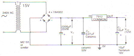
79XX three terminal
negative voltage regulators
The 79XX series are three terminal negative regulators with
fixed output voltages. The only external component necessary is a
compensation capacitor on the output.
These are essentially similar to the 78XX series positive regulators, with current limiting and thermal overload protection.
Specifications @25°C
|
|
LM7905 |
LM7912 |
LM7915 |
|
Output Voltage |
-5v ±.2 |
-12v ±.5 |
-15v ± .6 |
|
Line regulation |
5mV typ |
5mV typ |
5mV typ |
|
Quiescent Current |
1mA |
1.5mA typ |
1.5mA typ |
|
Power dissipation |
1.5W |
1.5W |
1.5W |
|
Input voltage maximum |
-35v |
-35v |
-35v |
|
Minimum input voltage |
7v |
14.5v |
17.5v |
Standard circuit
Page 54
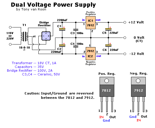
The use of a pair of the regulators (positive and negative) makes an ideal dual rail supply, for powering op-amps etc. A suitable circuit is shown below. This one uses 12V regulators, but obviously the voltage can be varied by changing regulators.
|
This list is only some of the most common types:
|
Page 55
Page 56
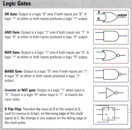
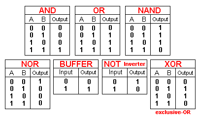
The above tables are called TRUTH TABLES. They give all the
possible outcomes for a particular gate.
The inputs are labeled A and B as shown above and the output is the
result of the inputs at HIGH or LOW level.
A HIGH is “1” and a LOW is “0.”
Page 57
4001 Metal Detector
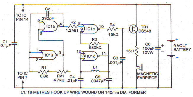
4001 is used in this circuit as two different types of oscillator. IC1a and IC1b with R1, RV1 and C2 form one oscillator. RV1 varies its frequency slightly. lCld, C4, C5 and L1 (search coil) form the second oscillator. IC18 acts as a mixer, combining the two oscillators and producing an output which is the difference between the two. This is amplified by TR1 and fed to a magnetic earpiece.
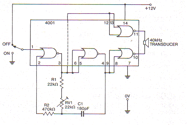
Ultrasonic Transmitter
The 4001 forms a complete 40kHz oscillator and driver for an ultrasonic transmitter. The oscillator frequency can be adjusted by means of RV1. Two gates act as square wave oscillators which then drive the other two gates in push-pull. These drive the transducer in push-pull to get the maximum.
Page 58
CMOS Logic Probe
The logic probe is an essential instrument for testing digital circuitry. This one uses only one 4001 IC, 3 LEDs and a handful of passive components. Power is obtained from the circuit to be tested. The first gate acts as an inverter by strapping its two inputs together. It is biased for half supply by R1. Under quiescent conditions neither LED1 or LED2 will light. If the input goes high, gate output goes low and LED1 comes on. If the input is taken low, the output of IC1 goes high and LED2 comes on, indicating a low signal. Short pulses are 'stretched’ by IC gates 2 and 3, producing a flickering output at LED3.

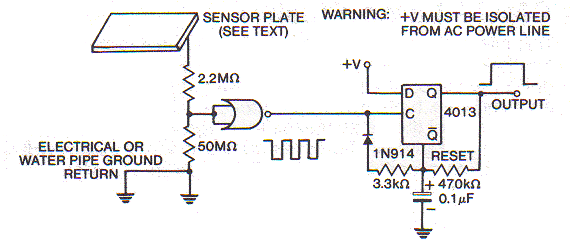
Touch Switch
The near infinite input
impedance of CMOS makes it ideal for use in touch and proximity
circuits. Usually a touch sensitive circuit needs physical contact,
while proximity circuit needs only the presence of an object such as the
human body. Touch sensors rely on three features of the human body. Skin
resistance is usually a few hundred thousand ohms, the body has a
capacitance to earth of around 300pF and the human body acts as an
antenna, picking up 50Hz power line fields. The figure below shows a
proximity switch based on human coupling of the 50Hz power line. A hand
very near the plate will induce hum onto the plate and this will be
passed to the circuit. The first gate is a 4001 with both inputs
strapped together. The hum will be squared up and used to trip the
retriggerable monostable as shown. A clean output results from the
instant of first proximity until a few milliseconds after release. The
sensitivity depends on the size of the plate.
The output of the 4013 can be connected to a relay via a transistor. It
could then be used to turn on a light or other piece of electrical
equipment. The 50M resistor can be made by putting 5M resistors in
series.
Page 59
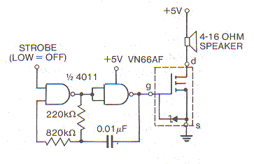
CMOS Lamp Flasher
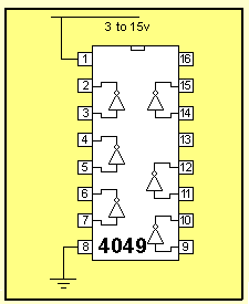
This circuit uses the four CMOS NAND gates of the 4011 as an oscillator and low power driver. The first two form a low frequency oscillator. All the gates are used with their inputs connected together. In this form they act as an inverter i.e. a HIGH produces a LOW out. The very high input impedance of the gates means that high impedance values can be used in the oscillator circuit. The power consumption is also very low and the circuit will function over the normal 3-15 volts range of CMOS.


Audio Alarm
Metal
Detector
This unit uses two pairs of 4011
NAND gates as two oscillators and two 4011 buffers. The search coil
oscillator has its frequency influenced by the position and proximity of
metal at the search head. The reference oscillator has its frequency
adjusted by the slug tuning of its coil and fine tuning by adjusting the
voltage on IC2c. The two signals are digitally mixed in one section of a
dual D-type flip-flop.

Page 60
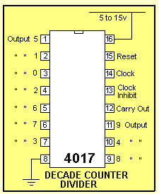
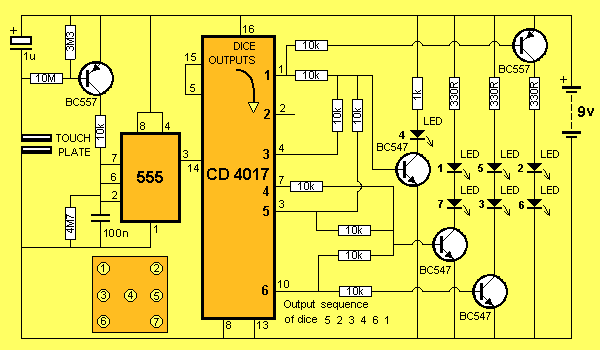
4017 CMOS Decade Counter/ Divider with 10 Decoded Outputs (Johnston Counter)
The CD 4017 is called a COUNTER or DIVIDER or DECADE COUNTER. It is a very handy chip for producing "Running LED effects" etc.
It has 10 outputs. For normal operation, the clock enable and reset should be at ground.
Output "0" goes HIGH on the rise of the first clock cycle.
On the rise of the second clock cycle, output "0" goes LOW and output "1" goes HIGH. This process continues across the ten outputs and cycles to output "0" on the eleventh cycle.
The "Carry Out" pin goes LOW when output "5" goes HIGH and goes HIGH when output "0" goes HIGH.
In other words, "Carry Out" is HIGH for outputs 0, 1, 2, 3 and 4. It is LOW when the following outputs are active: 5, 6, 7, 8 and 9.
When RESET (pin 15) is taken HIGH, the chip will make output "0" go HIGH and remain HIGH.
When "Clock Inhibit" (pin
13) is taken HIGH, the counter will FREEZE on the output that is
currently HIGH.
The clock signal must have a rise time faster than 5µsecs (VDD=15v).
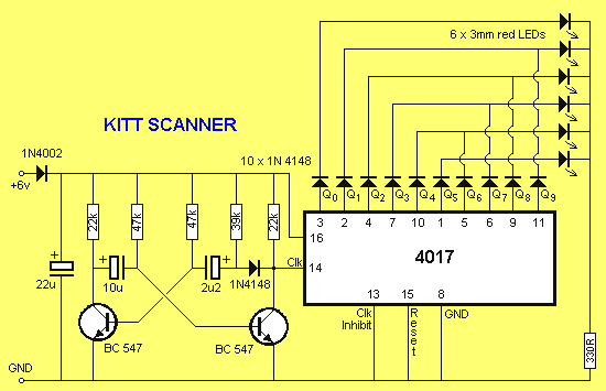
6 LEDs on the KITT SCANNER scan back and
forth similar to the
lights on the front of the KITT car in the movie.
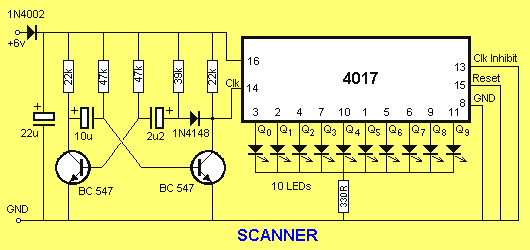
The 10 LEDs on the SCANNER turn on one-at-a-time, from left to right
LED DICE
Page 62


Logic Probe

This
completes Pages 42 to 64 of Data Book 1
http://www.talkingelectronics.com
Sept 2008 Nothing is copyright. You can copy anything
Colin Mitchell
to pages:
63 to 85