MULTI CHIP
PROGRAMMER
INTRODUCTION
NOW WITH ISP FEATURE
(In-Circuit
Programming)
IC-Prog 106B
& Help file - mentioned in
this article is an
old "burning" program.
Latest burning program: "WinPIC.exe" or "WinPIC.zip"
This programmer uses the 9-pin serial port (also called
the COM port or RS 232 port), found on desk-top computers.
For lap top computers, use a USB programmer:
PICkit-2 from:
Modtronix
(no kits for PICkit-2 programmer - only fully-built version)
You will also need MPASM and ".inc
files"
Set-up a folder called PICkit-2 in which you will place the
programs for all your projects.
Within the folder you can place
MPASM and ".inc
files" and PICkit-2
burning routine (from the CD that comes with PICkit-2).
If you are not using PICkit-2, call the folder All Files
and place "WinPIC.exe" or "WinPIC.zip"
in the folder,
as well as MPASM and ".inc
files."
You will need NotePad2.exe or
NotePad2.zip so you can take a .asm file from one
of
the projects we have produced and use it to write your own program.
sample.asm
sample.asm
Note 1:
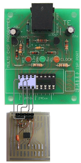
MPASM and WinPIC have been used to program PIC16F628A
using 8-pin to 5-pin adapter described below. The chip was programmed
successfully but WinPIC displayed "Programming failed and only the
first line of code was displayed in green. WinPIC does not
read the
chip properly after burning.
Note 2:
I have not successfully programmed a PIC10F220 via WinPIC
or PICkit-2. I do not suggest you buy a PIC10Fxxx until I have successfully
programmed one.
![]()
See lots more PIC projects and In-Circuit Programming
HERE.
![]()
This project
consists of 3 Pages plus a separate feature on Page 4, using Disasm
Program:
This project is designed to program the 8-pin PIC12c508A and 18pin PIC16F84
microcontroller chips to support the projects we have designed, however it
will also program a number of other 8-pin & 18-pin microcontrollers and the full list can be
seen when using IC-Prog. HOW THE CIRCUIT
WORKS The next new
point is how to use a transistor in a completely different mode to that
covered in our Basic Electronics
Course. But, suppose the
transistor is connected with a LED on the emitter AND collector as shown in
Fig: 3. This time, the current for the LED cannot come from the supply rail
(via the collector) and thus the base must supply the current. It is easy to
see that the lower LED is turned on via the current from the base. But the
interesting feature is the LED in the collector circuit will also come on
with the same brightness as the LED in the emitter circuit. With this basic
theory understood, you will be able to see how the Multi Chip Programmer
works, but before we get to the full circuit, Fig: 4 shows how the voltages
on the chip are developed with reference to the GND line.
Fig: 6 shows the complete circuit
diagram: The 2k2 resistor is fitted inside the 9 pin plug. This gives the
project 4 communication lines and thus 4-core telephone cable can be
used.
The transistor
on the Data line also operates in an unusual way. It functions in a
bi-directional mode, since the data must be transmitted into the chip when
burning and from the chip when reading. When delivering data to the chip, the DTR line goes
HIGH and the transistor is in emitter-follower mode. The input of the
chip will be high-impedance and the emitter voltage will be HIGH, being
pulled up by the 10k resistor and fed by the voltage from the DTR
line.
Once you know how the circuit works, you will feel much more comfortable about
working on it and/or modifying its operation. Go to: Construction
Page 1 - Introduction
(this page)
Page 2 - Construction
Page 3 - Using
the Multi-Chip Programmer
Page 4 - Disassembling
a .hex File This is a separate feature
using: Disasm
Program to
convert a .hex file into a .asm file.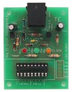
Click for
large photos
The Multi-Chip Programmer can now program Surface Mount chips and
PIC10F220 chips via
"WinPIC.exe" or "WinPIC.zip"
and the following
adapter: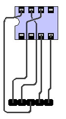
You will have to connect the 5 tinned-copper wires to the 8-pin socket
and 5-pin header, (called a "Machine Pin" strip or "header" similar to 5 pins
from a 24 "machine pin" IC socket).
The adapter connects
between the Multi Chip Programmer and
any of our projects that have the 5 "In-Circuit Programming" pins:
Connecting the Multi Chip Programmer to ICP
(In-Circuit Programming pins)
Note: IC PROG has now been
updated to WinPIC:
In
a nutshell, here is what you do:
1. Read the 3 pages of the Multi-Chip Programmer project.
It
needs a program called IC-Prog to carry out the burning
operation.
2. Buy and build the Multi-Chip
Programmer project.
3. Get IC-Prog.exe
file
and move it to your Desktop.
(download
IC-Prog.zip)
Latest IC-Prog 106B
Help file
4. Program a PIC chip, using the IC-Prog software. Connect
the Multi-Chip
Programmer to com1 and everything is ready to program a
chip. You will need a .hex file.
6.
For a list of .hex files click:
5x7 .hex files.
5. Read the notes on
Page 3 by Jason Williams, on configuring your
computer to run the software.
These files are for the 5x7 Display
project - but you can use any file.
If you want to convert a .hex file into readable lines of
code,
Page 4 has a disassembly program Disasm.
We could have called this project a "free programmer" to attract
your attention, but let's be fair, at the cost of a few dollars for the PC board plus a few on-board components and a lead, you
can call it a very low-cost programmer. With free software the project will
not only be the cheapest on the market, but it comes with full documentation
to get the absolute beginner into programming.
Why put it on the web?
The web is expanding at a phenomenal rate. By putting our projects on the
web, we are delivering them to the whole world. We have priced each kit to be less than buying the components separately. Once you work-out the cost of producing the board yourself and buying the parts from different suppliers, you will agree; it's cheaper
to send for a kit. We send everything out the same day and no matter where
you live in the world, air-mail delivery is only a long-distance
flight away. Buying is so simple. Simply send us an email to say you want to
buy a particular kit (we have over 200 kits)
and we will email you with the total cost including postage.
THE MULTI CHIP PROGRAMMER
This is a very simple project. It is a Multi-Chip Programmer that will burn a wide range of PIC
chips.
The PIC
Programming Course
has concentrated on the PIC12c508A and PIC16F84 chips as these cover the "beginners" end of the market.
The advantages of these chips has been fully documented in our articles and now we come to the
need to burn them.
Programming or Burning these chips is very simple and any project you design can include a 4-pin socket so that the chip can be programmed
"on-the-board." The 5x7
Display project is a typical example. It has a "burning socket" on-board for
a PIC16F84 chip. The only thing you have to remember when designing a
project, is to keep
pins 12 and 13 lightly-loaded so they can be used for the programming operation. If these lines
are used as outputs, the programming operation must be able to take them HIGH and LOW. Refer to the 5x7 Display
project to see how we have
designed the programmer section.
The '508A has not been catered for in the 5x7 Display project and so you need
the Multi-Chip Programmer to burn this chip and any others you want to
program.
The first thing
you have to remember . . . . this is not a normal circuit. A normal circuit
has a positive voltage connected to it and thus it has a supply rail and a
ground rail - the ground rail is called the zero volt rail.
In the Multi-Chip Programmer circuit, the supply voltage for the chip comes
from the RS-232 feature of the serial port. Some of the lines making up the
RS-232 are capable of rising to a positive voltage (about 8 to 12v) and
falling to a negative voltage (about -8v to -12v). There are also lines that
fluctuate from 0v to +5v . If all computers had a line that fluctuated between
+12v and -12v, the programmer circuit would be very simple. But
unfortunately some computers fluctuate between +8v and -8v. To make a circuit
that works on all ports was a challenge. The circuit we have used was
designed by JDM (http://www.jdm.homepage.dk/)
and full credit is given to him.
The chip requires a voltage of 13v on the MCLR
pin (between12v and 14v) to tell the chip to go into program mode. The chip does not require any
current on this line, just a voltage so the program mode can be invoked
(begin).
If one of the lines from the computer goes to +8v, and another goes to -8v,
they can be combined together to get a total of about 16v. This is more than
enough to create the necessary 13v.
This is the basis of how the circuit works and the reason for the diodes and
zeners.
But it's more complicated than that. The voltage-delivering lines are also
the lines that provide the signals to and from the chip during programming and reading modes. So, the circuit becomes
quite complex. The
lines delivering the signals are also the lines that charge the electro's.
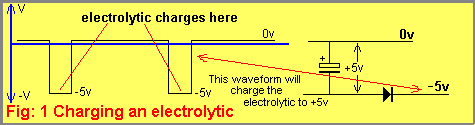
To understand how it works, we need to cover some basic theory.
If a line starts at 0v and moves negative to say -5v, it will charge an electrolytic
and the electrolytic will have 5v across it.
The circuit in Fig: 1 shows this:
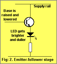
Normally, a transistor in emitter-follower mode is connected with the
collector to the supply rail and the base is raised and lowered from 0v to
supply voltage. The
voltage on the emitter is 0.7v lower than the base, but it has a higher
current capability than that delivered by the base. It's quite simple, the
current comes from the collector!
The normal emitter-follower circuit is shown in Fig: 2. (Also called common
collector)
The base-collector junction is reverse biased and will perform exactly like
the base-emitter junction. The base must supply the current for both LEDs
This is how the first transistor in the circuit is operating. The base is
supplying current to charge the 10u electrolytic and the 8v2 zener is
allowing the 10u electrolytic to charge to 8.2v higher than the 22u
electrolytic and supplying a voltage-reference for the MCLR
pin. The 10u electrolytic does not deliver its energy to the MCLR
pin, no current flows between the emitter and collector leads of the
transistor in this arrangement.
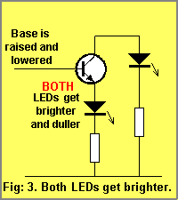
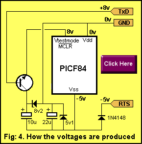
Fig: 5 shows
how the chip actually "sees" these voltages. You simply add 5v to
each of the voltages to make Vss = 0v. This makes Vdd = 5v and the
programming voltage = 13v.
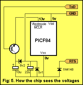
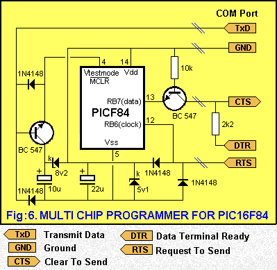
Fig: 7 shows how the transistor is
actually in an emitter-follower arrangement with the data line of the chip
on the emitter.
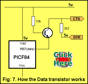
When the DTR line goes LOW, the collector of the transistor will go LOW,
because the only voltage supplying the circuit comes from the base. Since
the resistance on the base is 10k, and the resistance between collector and
ground is 2k2, the voltage division will produce about 1v on the collector.
Since the collector voltage goes LOW, the emitter voltage will also go LOW
as the transistor is in exactly the same arrangement as shown in fig: 3,
above.
Thus, by taking the DTR line HIGH-LOW, the data line of the chip will be
taken HIGH-LOW.
When the transistor is being read, the data appears on the Data line. This
time the DTR line is kept HIGH and when the data line of the chip goes LOW,
current is drawn through the collector lead. This current flows through the
2k2 resistor and produces a voltage drop across it. This voltage drop is enough
to bring the collector voltage down to about 1v or less and the CTS line
reads this as a LOW.
When the data line of the chip goes HIGH, current does not flow through the
2k2 resistor and CTS reads the line as a HIGH.
There are three more signal diodes in the circuit (the 4th diode has been
explained as it charges the 22u when RTS is LOW).
The diode on the MCLR line
takes MCLR LOW when TxD goes
LOW, while the other diode on this line prevents the voltage on TxD from
going below 0v.
The two diodes on the RTS line prevent the line going above 5v or below
0v.
Click on the diagram below to see an animation of the chip being set up for
programming and data being clocked in. This is only a simple representation
as the chip looks for 6 initial clock cycles and depending on the data it
receives during these 6 cycles, the chip will go into one of 9 different
modes. For instance, it can go into a mode called Load Configuration where
the next 16 clock cycles will load the Configuration Memory with the
necessary data bits.
The MCLR line must then be
taken LOW and HIGH again and the chip is ready to receive a different
loading mode. One of these modes is Load Data for Program Memory and
after 6 clock cycles the next set of 16 cycles will consist of a zero
start-bit, 14 bits of data and a zero stop bit.
As you can see, it takes a lot of cycles to get each byte of data into the
chip, but this is always the case when information is being
serial-fed.
At the moment we don't have any access to the software so you will not be in
a position to modify the operation of the program. But since it works
perfectly, I don't see any need for modification.
![]()