SPOT
THE MISTAKES!
Page 3
Page 1
Page 2 __
Page 4
Page 5
Page 6
Page 7
INDEX
![]()
Here's a circuit from the web. It has obviously never been tried: Can you spot
the mistake?
Here is a description of the circuit as supplied from the website: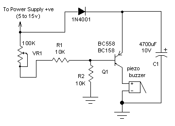
Fig 27. Power Supply Failure Alarm
This circuit can be used as an alarm for power supplies in the range of 5V to
15V.
To calibrate the circuit, first connect the power supply (5v to 15v) then vary
the potentiometer VR1 until the buzzer goes OFF.
Whenever the supply fails, resistor R2 pulls the base of transistor low and
saturates it, turning the buzzer ON.
The fault in Fig: 27 is R2. It forms a voltage divider with VR1 and R1. The
voltage on the base will always keep Q1 turned ON.
Q1 is a PNP transistor. To turn the transistor ON, the base voltage must be
0.7v below the supply rail. The pot (VR1) and R1 form a voltage divider with R2
and to see why this circuit will not work, we need to remove the transistor.
The voltage at the point where the base is connected, will be about 50% of the
supply voltage or less, due to R1 and R2 being a voltage divider to produce a
50% voltage. The inclusion of the pot will reduce the voltage further. This will keep the buzzer ON.
By removing R2, the circuit will work perfectly. This is shown in Fig 28:
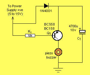
Fig: 28. The corrected Power Supply Failure Alarm
When the supply drops more than 1v, the piezo buzzer will start to come on. The
piezo buzzer needs to be an active type (not a piezo diaphragm). It needs to contain an oscillator circuit and produce a loud squeal or beeping sound
when a DC voltage is supplied to its terminals.
The purpose of the diode is to prevent the charge on the electrolytic being
passed to any other part of the circuit when the power fails.
The electrolytic will be charged to 0.7v less than the power supply, due to the
presence of the diode and thus the base voltage must fall 0.7v plus the
base-emitter (0.7v) voltage ( =1.4v ) before the transistor will begin to turn on.
When the power supply fails, the base will be taken to 0v via the 10k
resistor and the transistor will be turned on. This is activate the buzzer.
Hearing Aid
The most obvious mistake is the direct connection of the collector of Q3 to the
base of Q4.
The output is push-pull and consumes less than 3mA (with no signal) but drives
the earpiece to a very loud level when audio is detected.
Now back to our first point. What is the purpose of the 1R resistor?
It is now obvious to see what is happening. The output transistor is in
emitter-follower mode and is being pulled up via the driver transistor. The 1R
resistor will not have any effect on the circuit.
On the other hand, our design is fitted across one of the door switches and no
alteration of the wiring is needed. All doors will provide the interior-light
delay and it's a simple procedure to fit our circuit.
This next circuit also comes from the web.
Again, it has never been tested as it has a number of glaring mistakes: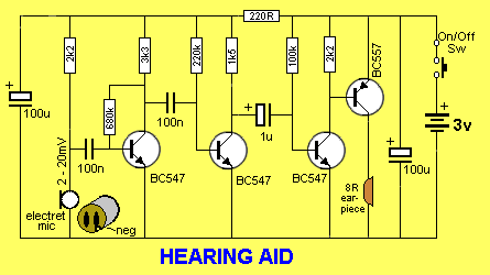
Q3 is turned on all the time via a 100k resistor and if the transistor has a
gain of 100, the collector-emitter will appear as a resistor with a value about
one-hundredth of the base resistor - namely 1k.
Q4 will also be turned on and the emitter-base voltage drop will be about 0.7v.
This means the 1k resistance of Q3 will appear across the rail and consume
2.3mA. This is wasted current.
Q2 is also turned on all the time and consumes current. By contrast, Q1 is only
partly turned on as the collector will be at approx mid-rail.
Since a hearing aid is on for
a long period of time, the current consumption should be as low as possible as
the batteries must
be small and therefore have only a limited amount of energy.
The circuit needs to be re-designed to consume the least current.
The following circuit shows these improvements: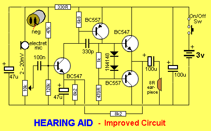
Fig 30: The improve Heading Aid circuit
The whole circuit is DC coupled and this makes it extremely difficult to set
up.
Basically you don't know where to start with the biasing. The two most critical
components are 8k2 between the emitter of the first transistor and 0v rail and the 470R resistor.
The 8k2 across the 47u sets the emitter voltage on the BC 547 and this turns it
on. The collector is directly connected to the base of a BC 557, called the
driver transistor. Both these transistors are now turned on and the output of
the BC 557 causes current to flow through the 1k and 470R resistors so that the
voltage developed across each resistor turns on the two output transistors. The
end result is mid-rail voltage on the join of the two emitters.
When setting up the circuit, the first thing you aim for is mid-rail voltage on
the emitters.
With a circuit such as this, the most important factor is stability. It is very
easy to create unwanted instability called "motor-boating" or "self-oscillation" due to
a signal (waveform) on the
power rail being detected by the front end and getting amplified to a point
where the resulting amplitude completely over-rides the audio you are tying to
detect.
The 8k2 feedback resistor provides major negative feedback while the 330p prevents
high-frequency oscillations occurring.
Car Interior Light
The next circuit comes from a
monthly electronics magazine. It contains two things that need discussing. The
first is the need for the 1R resistor. And the second is the difficulty in
implementing the circuit. 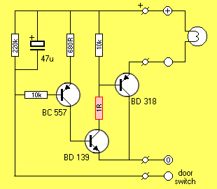
Fig 31: Car Interior light Delay
Let's take the second point:
The circuit is designed to turn off the interior light of a vehicle, about 30
seconds after the door has closed. It is connected to the interior light and
some re-wiring of the car has to be done to fit the circuit.
Since two or three doors of the modern car are connected in parallel to the
interior light, it is difficult to see how this circuit will work. How is the
second and third door connected to the circuit? The article does not explain
the difficulty in implementing the circuit.
Q3 is in emitter-follower mode and the base current is always less than the
collector-emitter current. It is only normally about 1%, but can be up to 10%.
In other words, only a very small current will flow though the base, so why put
a low value resistor on it?
It may be difficult to see what is happening, so we will invert the output and
show it as follows: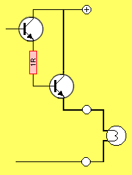
Simply pull out one of the door switches and connect the circuit to the wire
connected to the switch and an earth wire. The circuit can be made on a long
thin board that can be heat-shrunk and pushed through the door-switch hole and
the switch replaced. It's as simple as that. 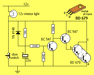
Fig 32: Courtesy Light Extender
There are two ways to produce a Push-Pull arrangement. These are shown
below:
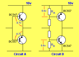
Fig 33: Two push-pull output circuits
First, a little theory behind Push-Pull.
The animation isn't entirely accurate but it shows the signal driving one
transistor at a time and being passed to the speaker via an electrolytic. The
electrolytic is charged and discharged a small amount during the processing of
a signal and forms part of the signal entering the speaker during the time when
the lower transistor is turned on.
Can you see the fault?
CURRENT
The corrected circuit. Note how simple the diagram becomes. Only one arrow is
required for current. Multiple arrows are used when electrons are being
identified.
Circuits A and B are called basic arrangements. Note the placements of
the PNP and NPN transistors. They are placed differently in each circuit.
The circuits are called Push-Pull as the two output transistors are
taking it in turns to deliver energy to the load. The transistor arrangement is called
Complementary-Symmetry.
To produce speech or music from a low impedance device such as a
speaker, the driving circuit must be capable of delivering a high current to
get volume from the speaker and the waveform must follow the original signal to
prevent distortion.
For the speaker to produce a loud volume, it requires energy (power) and since
the supply voltage is low, the current must be high to obtain a driving force
called watts.
The following animation shows how the input waveform is passed to an output
device such as a speaker: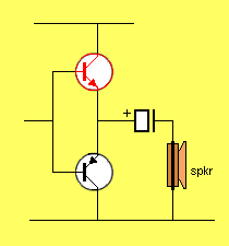
Fig 34: Driving a speaker
In circuit A, the input and output are in-phase. This just happens to be so. It
is not an important factor in this discussion. When the input rises, the top
transistor is turned ON and pulls the emitter up. If the output is at say 1.7v
(as a result of a previous cycle), it will start to be pulled up when the input
is 1.7v+ 0.7v = 2.4v
The input can generally rise no higher than 90% of rail voltage (1v below
rail voltage in the example above), so the output rises to 8.3v
When the input is 0.7v below the present state of the output (8.3v), the lower
transistor is turned ON and pulls the output down to 1.7v
This gives the output a range of 6.6v for a 10 rail. At the moment we are not
concerned with the output voltage range or the efficiency of the circuit.
We just need to see how the output follows the input. The animation above shows
this.
Circuit B operates slightly differently. The first thing to do is create a
voltage divider with 4 resistors so the voltage across each base is 0.6v when
the input is at mid-rail.
This must be done to keep each transistor turned OFF during quiescent
conditions (mid-rail conditions) and prevent them both coming on at the same time during any
part of the cycle.
The voltage across Ra and Rb is created by selecting the correct value for each
of the 4 resistors. We will not go into the mathematics of this, at the moment.
When the input rises, the lower transistor will come on and the voltage on the
output will fall. The input only has to rise a small amount for the voltage on
the base to increase to the point of turning the transistor ON.
As the input rises further, more current will enter the base and the transistor
will be turned on fully.
Further increase in the input voltage will have no effect on the output-level.
The transistor is already fully turned-on.
When the input voltage falls below mid-rail, the situation applies in reverse
and the output voltage rises.
This means the output ranges from 0.5v to 9.5v and the input voltage only needs
a swing of about 1.5vp-p to achieve this.
The output of circuit B is out-of-phase with the input and and provides a
voltage-gain as well as a current-gain.
Now we come to the problem:
The following push-pull circuit was presented in a magazine recently. It has a major
fault: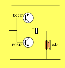
Fig 35: The faulty push-pull circuit
The two transistors are in the wrong positions.
The two bases are joined together and the base-emitter voltage cannot rise
above 0.7v.
The two transistors will be instantly damaged. 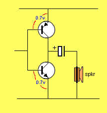
Fig 36: The two transistors will be damaged
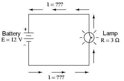
The next circuit has been taken from a "book" on the web.
As far as I am concerned, it contains a number of mistakes.
The author has written a long discussion on the direction he has chosen for
"current arrows" and why he has chosen "current flow" from negative to
positive.
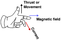
The facts are these. The argument between CONVENTIONAL CURRENT FLOW and
ELECTRON FLOW has been discussed and concluded many years ago.
It is now accepted that ELECTRICAL circuits show conventional current-flow with
current emerging from the positive terminal of the battery.
It is also accepted that any arrow on an electronic circuit represents
CONVENTION CURRENT.
When you place a multimeter (switched to current) on a circuit with the
positive lead nearest the positive terminal of the battery, the needle reads
"up-scale." Why show a circuit diagram with current flowing in one direction
and a multimeter showing current flowing the other direction????
There is no point confusing students by being "one-out" and presenting
current flowing in the opposite direction. How are you going to apply Flemings
Left-Hand rule if you don't know the direction of the current?
The other notation I do not like is attributing the letter "E" to a
normal battery.
The concept of "E" is "Electromotive Force" and applies to a voltage source
that has little or no ability to deliver a current.
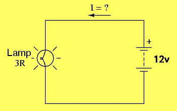
In addition, the battery symbol is incorrect on the diagram below. It should be as shown in our
corrected diagram. If you want to be pedantic,
the circuit diagram should also be reversed as the battery or supply is traditionally shown on the right.
The idea of teaching electronics is to present complex items in a way that students comprehend
them as quickly as possible. It's not to
cause frustration at every turn.