SPOT
The next discussion is not a mistake but an item that needs discussing.
It is a 555 demonstration board.
ADJUSTABLE VOLTAGE
STRESS METER
THE MISTAKES!
Page 5
Page 1
Page 2
Page 3
Page 4 ___
Page 6
Page 7
INDEX
![]()
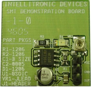
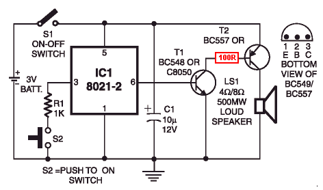
It is designed to teach beginners how to solder surface-mount components. It
should also teach how to lay out a circuit so it is easy to follow.
The circuit is an absolute jumble.
For a start, the power plug is not polarised and if it is inserted around the
wrong way, the chip will be damaged.
It should be a 4-pin plug with the "OUT" terminal in the centre, so the GND
pin can be at the bottom.
Secondly, the layout should follow the circuit diagram. For a simple project
such as this, it would be much easier for the beginner to see each component
in the same relative place as on a circuit diagram. This involves turning
the chip around so it sits correctly, and placing the parts so you can where
they belong, relative to the timing circuit.
These are the skills we are teaching on this website. The whole object of a
good design is to make it easy to service the product - not create
frustration.
Mat Switch
Here is a circuit from an Indian Magazine: "Electronics For You."
Take the following circuit for example. It is a MAT SWITCH and is designed
to operate a Piezo buzzer for 50 seconds, after someone has put their foot
on a mat.
The designer of the circuit has not thought "outside the box." The circuit
uses a 9v battery. When at rest, the circuit draws at least 10mA. How long
do you think a 9v battery will last?
What an absurd waste of current.
Now we look into the design faults:
The touch pads consist of conductive foam, such as that obtained from the
foam used to pack sensitive IC's.
The article suggests two small pieces of conducting foam. Where are
you going to put small pieces of foam in a mat?
You will need a large piece if you want to guarantee to detect pressure.
The next point is: What is the purpose of the resistor and capacitor on
the emitter of the first transistor?
Secondly: What is to prevent the base of the transistor floating and picking
up static electricity and false triggering the circuit?
Thirdly: Why is the resistor on the base of the first transistor so low?
It should be 10k to 100k.
Overall, the circuit serves no practical purpose. A 9v battery would be flat
in a day. And at $2 per battery, how many Indians are going to replace the
battery every day!
It makes you laugh!
We have designed a far-superior circuit using a CD 4001 or CD 4011 and it
draws one microamp!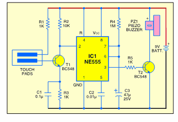
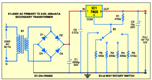
Here is another "Electronics For You" circuit. It has a very dangerous
mistake. When the selector-switch is changed from one setting to another,
the output temporarily goes HIGH and this puts a very high voltage on the
equipment you are powering.
If you think a 9v AC transformer will provide 12v DC from a
7805, you are kidding yourself. The 7805 needs at least 2-3v for regulation
and a 1amp transformer has a regulation problem of at least 1v. The circuit
is a real disaster!
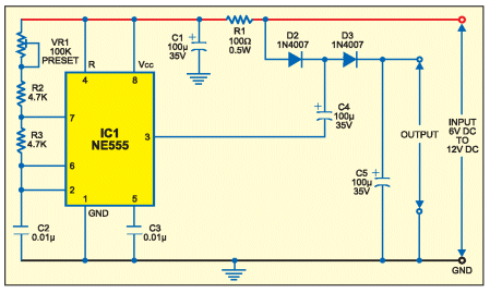
VOLTAGE DOUBLER
And yet another "Electronics For You" circuit. In fact every project from
their website contains mistakes and designs that are far from the normal.
The circuit below is a Voltage Multiplier. But the actual
voltage-multiplying section is the part that concerns us.
The output of a 555 is capable of sinking and sourcing about 200mA and it
can be connected directly to a "charge pump" as shown in the second diagram.
This saves 2 transistors and 3 components. The only problem with using the
output of a 555 IC is the voltage swing. The output rises to 2v below rail voltage
and only goes to 2v above the 0v rail. In other words, you lose about 4v.
This means the rail voltage for the project needs to be higher to get the
required output voltage.
The author has used a BC 548 to charge the 100u, and a BD 139 to discharge
it. Why use a "power transistor" to discharge the electro? It doesn't make
any sense. Also, why use a 1N 4007 diode for a 12v circuit? The 1N 4007 is a
high voltage diode. It looks like the author had a lot of junk parts in his
parts-box and threw them into the project. This is the sort of "poor
presentation" that I don't like, since a newcomer will wonder why each of
the components has been chosen and will get a false understanding.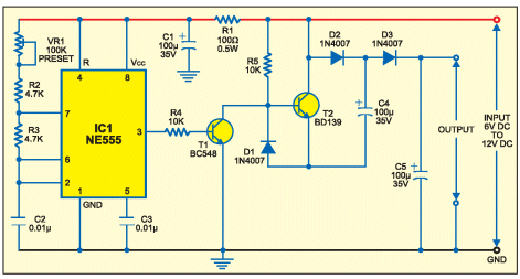
In the next circuit from EFY, we have a Stress Meter. The author claims the
transistor is a common-emitter configuration, however it is actually an
emitter-follower. But the point of this discussion is the purpose of the
560R resistor and diode.
The author claims they are biasing components, however they don't serve any
purpose at all.
When designing a circuit, you need to go over every component and say "is
this necessary?"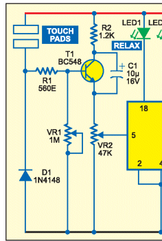
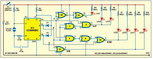
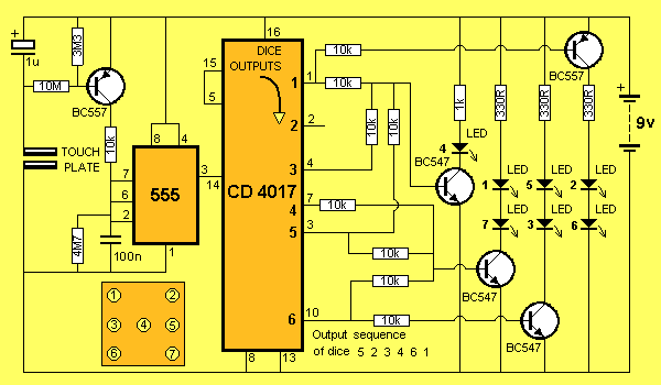
LED DICE
The next circuit uses "gates" (NAND and NOR gates) to drive a set of
LEDs to form the spots on a Die or Dice. A CD 4001 or CD 4011 is not capable
of delivering enough current to drive two LEDs in parallel. The brightness
will be very small. The second
circuit uses transistors to drive the LEDs. It only uses two IC's and has a
slow-down feature.
The motor is driven from a pair of 555 IC's. Apart from the fact that 555
IC's can only deliver about 200-300mA, the maximum output voltage is about
2v lower than rail voltage. The "LOW" is about 2v above the 0v rail. This
means the 9v motor will get a maximum of 5v from a 9v supply. The motor will
deliver almost no torque at all.
The circuit has an "H-Bridge" to drive the motor. The top left-hand
transistor is an emitter follower. The base must be taken to nearly rail
voltage so the emitter can rise and deliver a positive voltage to the
motor. But the Q line is limited to a rise of 0.6v since it is connected to
the base of the lower right-hand transistor!
When the BC 547 transistor is turned on, the resistance between the
collector and emitter is very low. The BC 547 turns on the BC 557 and the
voltage drop between the base and emitter of the BC 557 is 0.7v. This means a high current
flows across the base-emitter junction of the BC 557 and between the
collector and emitter of the BC 547. A current-limit resistor is needed as
shown in the diagram below. This will limit the current and yet allow the
circuit to operate correctly.
Sometimes it is very difficult to "see outside the box." That's why you have
to come back to a circuit and look at it over and over again.
Motor Driver
In the next circuit from EFY, we have a Motor Driver circuit: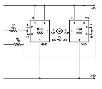
I have written to the Indians who have designed these circuits and received
no reply.
They have actually put these circuits into magazines with a readership of
500,000. Pity the poor readers!
None of the circuits I have presented, have ever been prototyped or used for
a period of time to determine if they contain errors or problems.
This is one of the most important things for a design-engineer to do. He
must test everything TO DESTRUCTION!
Actually I am only kidding, but you must test everything for hours and hours
and give samples to friends to try.
I could not resist the next EFY disaster: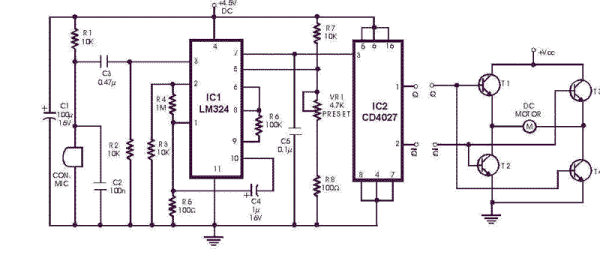
This circuit obviously has never been constructed and unless you build a
circuit and try it, you will be embarrassed too.
Music Chip
We have covered the next fault on page 4 of this article, but it is worth
mentioning again.
It comes from EFY:
I have seen lots of stupid circuits but I have also seen a lot of very
clever designs.
To become a good design-engineer, you have to study thousands of circuits
and see how and why they work. You also have to see the problems of "others"
so you don't make the same mistake.
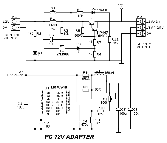
12v Adapter
The next discussion is a general mistake. The diagram below has no component
values. When you look at the diagram, you have absolutely no idea how the
circuit works as the value of each component gives you and idea of the
current flowing and how the components are biased. The list of components
has been placed on another web page and this makes diagnosis very difficult.
A circuit diagram should be as complete as possible. It is difficult to see
how you can get 12v out (after regulation) from a 12v supply. The diagram
below shows the component values added to the circuit. 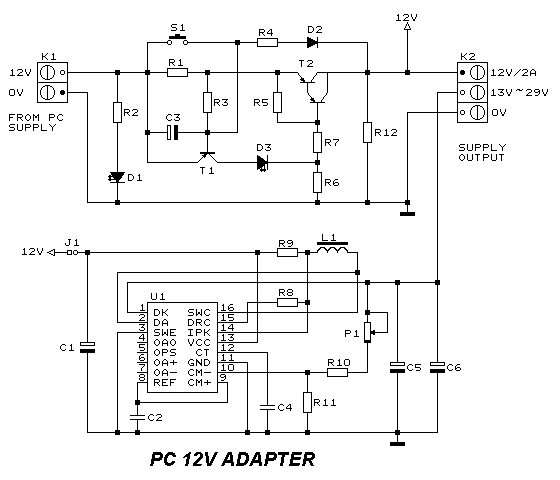
PC 12V ADAPTER
Item Quantity Reference
Part
______________________________________________________________________
1 3
C1,C5,C6 100uF 25V LOW ESR
2 1 C2
100nF
3 1 C3
10uF 16V
4 1 C4
470pF
5 1 D1
LED GREEN 3mm
6 1 D2
1N4148
7 1 D3
LED RED 3mm
8 1 J1 JUMPER 2 PIN
9 1 K1
PLUG-IN TERMINAL BLOCK 2 WAY
10 1 K2
PLUG-IN TERMINAL BLOCK 3 WAY
11 1 L1
150uH TOROID CORE INDUCTOR
12 1 P1
100K MULTITURN
13 1 R1
0R33 3W
14 1 R2
1K5
15 2 R3,R4
10K
16 1 R5
560R
17 2 R6,R7 1K
18 1 R8
180R
19 1 R9
0R33
20 1 R10
82K
21 1 R11
8K2
22 1 R12
5K6
23 1 S1
PUSH SWITCH
24 1 T1
2N3906
25 1 T2
TIP147, BD902
26 1 U1
LM78S40