|
The |
Before I start, I want to
say why I have criticized so many YouTube videos and
University lectures as being totally worthless and inaccurate.
Most of the videos use a gain of 100 for the transistor, whereas the
transistor may have a gain of 200 to 250. But due the biasing
components, the final gain of the stage is about 70. Thus, none of their
calculations will be accurate. And when a transistor is passing its
maximum current, the gain can drop to 50 or even less than 10.
(The same with frequency. When a circuit is operating at a high
frequency, the gain of the transistor falls to ONE !! when
operating at the maximum frequency that the transistor can operate at.
In other words it has NO GAIN.)
So, you
have absolutely no idea what the circuit will produce.
Second, none of the videos take into account the specifications of the
input device or the details of the item that will be connected to the
output of the stage.
It is absolutely worthless, going into a lot of accurate calculations
when the output will be completely different.
Their commitment to detail and working things out to fifteen decimal places is absurd.
Once you read all my articles you will see how you have been "lead down the garden path" with all this irrelevant mathematical concoction.
In the real world, things are done completely differently to anything you have learnt and the only way to get an accurate result is to build the circuit.
The Transistor Potentiometer
In this article you are going to learn to "see" the transistor as a variable resistor - a Potentiometer and this will change your whole perspective of seeing how a circuit works.
I can see the operation of every circuit "in my head."
Forget all the RUBBISH you have seen and learnt and read in text books and on the web.
None of it will help you understand and design and "see" how a circuit works.
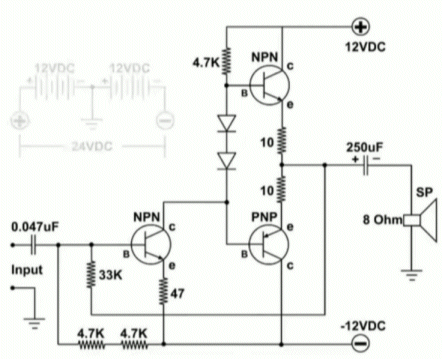
I bet you have never been told a transistor does not deliver energy to the following stage. It is the LOAD resistor that delivers the energy. I call it: "failure by omission." None of the writers have ever designed or repaired a project. They simply repeat what they have read and been told.
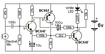
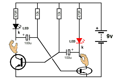
Go to the following link to see the description of the circuit:
https://www.talkingelectronics.com/projects/200TrCcts/200TrCcts.html#77a
and then return
The circuit above is very complex and the inclusion of the 100u feedback
electrolytic is almost impossible to work out.
But we can start with the
principle of how a transistor REALLY WORKS.
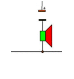
A transistor is just a VARIABLE RESISTOR - a POTENTIOMETER
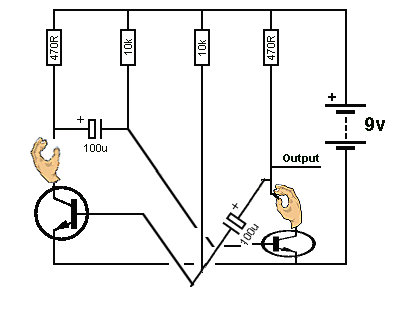
Here is the circuit of a REAL TRANSISTOR:
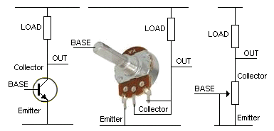
Fig2: The Transistor is
simply an adjustable resistor
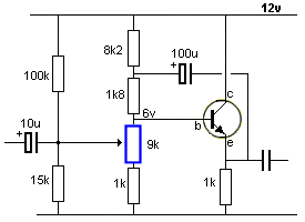
Simply replace the transistor with a POTENTIOMETER. In the next diagram we have changed the transistor into a "pot."
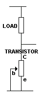
Fig3: The circuit becomes
2 resistors
You now have two resistors in series.
Two RESISTORS IN SERIES is the basis of a VOLTAGE DIVIDER. And that is
what each section of a circuit becomes. It becomes a VOLTAGE DIVIDER.
Now I can tell you the most radical comment you will ever hear. The
potentiometer cannot produce any amplification. No voltage amplification
and no current amplification. And a transistor cannot produce any
voltage or current amplification, by its self. It need one or more
resistors.
Mainly, it is the LOAD RESISTOR that provide and produces and assists and is
essential in creating these features.
And only when you realise the LOAD RESISTOR creates all the magic, will
you understand how a circuit REALLY WORKS.
Just because the transistor increases the base current by 100 or 200,
does not make the circuit "move" or "work."
The whole circuit works on the VOLTAGE DIVIDER principle.
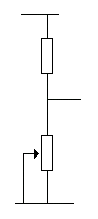
Fig4: The VOLTAGE DIVIDER
The VOLTAGE DIVIDER is simply two resistor in series. When the lower
resistor is a VARIABLE RESISTOR the voltage at the join will INCREASE or
DECREASE.
When the resistance of the variable resistor increases, the voltage at
the join increases.
That means: when the resistance of the transistor increases, the
output voltage increases.
But you must understand this as: The top resistor PULLS the
voltage high. The transistor merely ALLOWS the LOAD resistor to pull
the output voltage HIGH.
Now, depending on the value of the LOAD RESISTOR, and the ability of the
transistor to pull the output voltage LOW, the amplitude of the output
is created. The transistor PULLS the output LOW and the LOAD RESISTOR
pulls the output voltage HIGH.
But the LOAD RESISTOR can only pull the output voltage HIGH when the
transistor stops pulling it LOW.
If the transistor can "pull-down" very strongly, the LOAD resistor can
be a small value of resistance and this means the current in the circuit
will he high.
THE
VOLTAGE-DIVIDER LAWThe Voltage-Divider LAW is also known as the Voltage-Divider Principle or
The Voltage Divider Concept or
The Voltage Divider Rule.
It refers to a circuit with DC voltage across it - a battery voltage.
The voltage across each component will depend on the resistance of each component.
Low resistance components will have a small voltage across them and high resistance components will have a high voltage.
The addition of each voltage will the voltage of the battery - called the SUPPLY or RAIL VOLTAGE.
The DC voltage will see the resistance of each component. That's simple for resistors, but for capacitors, the actual voltage across it will be detected and added to the list. An inductor will have a DC resistance and will be treated as a resistor. A transistor will be treated as a resistor (as explained in this article) and a diode will have a resistance that usually gets converted to 0.7volts.
The voltages are "magically" generated and add up to the battery voltage and the resistances are added and by Ohm's LAW, the circuit allows the exact value of current to flow.
We can work out this value of current when the circuit contains resistors but it is more difficult when transistors and diodes are involved.
This article will help you work out the difficult circuits. The secret is to see every component as a resistor (resistance).
HOW DOES A CIRCUIT WORK?
Back to the circuit above . . .If the LOAD RESISTOR is a high value of resistance, the transistor
will find it very easy to pull the output down to a low value. And this
means only a small current will be present.
If the LOAD RESISTOR is a very LOW value of resistance, the transistor
will not be able to pull the output down AT ALL (if the transistor is
weak).
The input lead of the transistor is the BASE and it needs CURRENT.
Current has MUSCLE and it will turn the shaft of the variable resistor
to produce a LOW VALUE of resistance.
In actual fact, the transistor increases the "strength" of the input
current 100 times (or more) to turn the potentiometer shaft.
THE NEXT POINT
Repeating: If the value of resistance of the LOAD
RESISTOR is HIGH, only a very small current will flow in the voltage
divider and only a very small current will be available on the OUTPUT.
If the value of resistance of the LOAD RESISTOR is SMALL, a HIGH
current will flow in the voltage divider and a HIGH current will be
available on the OUTPUT.
This means the output current will depend on the value of resistance of
the LOAD RESISTOR. As long as the transistor can pull the output voltage
down to a very small value, the value of current depends only on the
LOAD RESISTOR.
You also have to understand the output voltage
depends ONLY on the LOAD RESISTOR, (when the
transistor is able to pull the output voltage LOW).
So, all we have to do make sure the transistor can pull the output
voltage LOW and the amplitude and output current capability will depend
on the value of the LOAD RESISTOR.
Now, T
HE NEXT POINTHere's the next amazing thing:
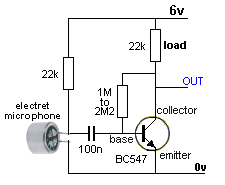
Fig5: The
Self Biased Transistor Amplifier
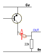
We will take the Self Biased Transistor Amplifier and see how it works.
When the stage is sitting with no audio input, nothing will be
processed.
But a tap on the microphone will reduce is resistance (impedance) and
the voltage to the 100n coupling capacitor will fluctuate up and down
and when the cycle produces a rising voltage, the first 22k LOAD RESISTOR will do the "pulling up."
Now, what we say is: 22k is entering the transistor
amplifier and the transistor reduces this value by 100 to 200 - as this
the gain of the transistor - and it becomes 22,000/100 = 220 ohms.
That's right!! The transistor deals with the input and turns
it into a 220 ohm resistor, exactly like fig6:
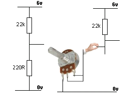
Fig6: 22k:220R voltage divider and the pot
pulling the 22k DOWN.
All you have to do is work out what voltage will appear at the join and
you will find it is only a very small voltage and that's how the circuit
has the potential to produce a very good output waveform. And if I go
into further investigation I will get a very accurate outcome without
any mathematics or equations or frustration.
I will get a much closer result than any mathematician because I KNOW
WHAT I AM DOING.
Technically we have not achieved much in this circuit because the first
load resistor is the same value as the second. But we have created an
increase in amplitude. But the main aim for each stage is to
create an increase in current. Otherwise the stage is called an
INTERFACE STAGE to connect two items with different impedances.
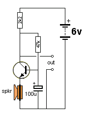
Here is another way to see how the transistor works: The electret
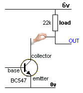
microphone and self-biasing components have been removed to simplify the
discussion.
When current enters the base, the transistor is able to increase this
current by 100 to 250 times, depending on the gain of the transistor.
This means the transistor can "reach out" and deliver this current
to the LOAD. The load is 22k. Suppose 0.001mA is
delivered to the base and the gain of the transistor is 200. This means
the "hand" will deliver: 0.000001 x 200 = 0.0002A to
the 22k. (0.2mA) By Ohm's Law, a voltage will be developed across the 22k of:
{V = IR} = 0.0002 x 20,000 = 0.2 x 20 = 4v
This means the collector voltage will be 2v.
Now we come to the most
important part of the discussion. This has NEVER been covered before in
any text book or University discussion.
When the transistor turns ON and lowers the voltage on the collector,
the output voltage falls and no energy is passed to the next stage in a
circuit.
It is only when the input voltage falls and the transistor turns OFF,
the output voltage RISES and energy is passed to the next stage. This
energy is delivered by the LOAD and not the transistor.
It is the collector LOAD resistor that passes energy to the next stage.
"PULLING UP" and "PULLING DOWN"
When we say the
circuit is: "pulling the resistor down" we mean the circuit is pulling the
voltage on the bottom of the resistor to a lower value.
Here is an example:
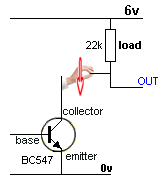
In the circuit above, the transistor can only PULL THE OUTPUT VOLTAGE DOWN. When the transistor stops doing this, the LOAD resistor pulls the output voltage up. The transistor DOES NOT pull the output voltage UP. The resistor does this.
The only way the transistor can "pull the resistor down" is to increase
the current through the resistor. The increased current creates a larger
voltage across the resistor and this lowers the voltage on the bottom of
the resistor.
This is the same as allowing the transistor to turn ON more.
The same applies to "pulling a resistor UP:"
The transistor has to deliver more current through the 22k to produce a
higher voltage across the resistor and thus the output voltage rises.
The transistor DOES NOT push the output voltage DOWN. When the
transistor turns OFF, the resistor pulls the output voltage DOWN.
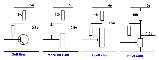
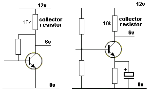
LARGE and SMALL TRANSISTOR GAINS
All transistors have a gain - the ability to AMPLIFY. That's why
they are used is a circuit. This gain can be from 10 to 700, depending on
the transistor and the current it is passing via the collector-emitter
leads.
You have no idea of this value and only sometimes does the data sheet
provide a range of values.
Now we are going to show how a low value of gain and a high value of
gain affects the collector voltage, (without changing any of the circuit
values).
The same applies to the H-Bridge circuit.
COMMON BASE
The most difficult stage to understand is the common-base arrangement
because no-one has described it simply.
Read the following article and then
return
We will use the following circuit:
This circuit operates in a completely different way to
all the other configurations. The gain of a the transistor in a
common-base arrangement does not come into the operation of the circuit.
It merely transfer the current produced by the speaker when it is used
as a dynamic microphone to pick up sounds in the room.
When the cone is pushed, the dynamic mic produces a positive voltage.
When the cone moves in the "out" direction, it produces a negative
voltage. This is called an "AC waveform" and corresponds to the
sound it is is receiving.
At the start of our discussion, the transistor is biased by the 2k2 and
47k and current flows through the microphone. This puts a very slight
voltage on the emitter.
The base cannot move up or down because it is connected to a 100u
electrolytic.
When the microphone hears a sound, it produces both a positive voltage
and negative voltage.
Suppose this is 1mV. We can only easily measure voltage changes and we
have detected 1mV decrease, when the cone moves in the "out" direction.
This decrease will turn the transistor ON (as discussed in the
this link).
The transistor is a current handling device and we need to convert 1mV
across 8 ohms to a value of current. This is: I
= V/R = 0.001/8 = one eighth of a
milliamp.
The transistor will pull the 2k2 load resistor DOWN until an extra one
eighth of a milliamp flows in the resistor.
The increased voltage across the 2k2 is: V = I x R
= 0.000125 x 2,200 = 0.275V = 275mV.
The transistor has increase 1mV to 275mV due to the value of the LOAD
RESISTOR. The gain of the transistor does not come into the equation.
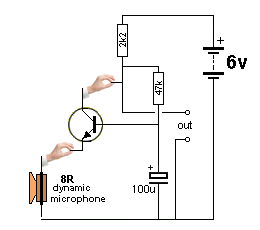
The amount of (reduced) current that flows in the
emitter is the same as the amount of
increased current that flows in the collector.
In conclusion, the gain of a
common-base arrangement is the value of the LOAD resistor, dividend by
the value of the emitter resistor. In this case: 2200/8 =
275.
ANOTHER EXAMPLE
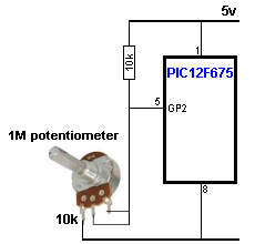
That's why you have to see the IR transistor as a variable resistor ,, ,
as shown in the following diagram.
When the potentiometer shaft is rotated to full resistance, a
voltage-divider is set-up between the pot and 10k load resistor. . . . .
. . 10k is in series with 1Meg ohms. You need to understand voltage
dividers and very little voltage will be "dropped" across the 10k.
If the supply is 5v, pin5 of the micro will see 4.95v
The solution is to increase the LOAD resistor to 100k. The voltage
at the join of the resistors becomes 100k:10k and to keep things
simple, the voltage across the 100k is 4.5v and the input of the
microcontroller sees 0.5v. This is low enough for the micro to register a
LOW.
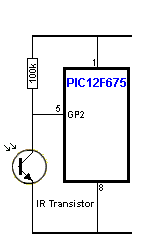
This is the IR transistor and 100k LOAD:
Here's the way to look at the circuit. The IR transistor can only pass a
certain amount of current.
The Infra-red transistor is "very weak." It does not have a strong
ability to "pull" the resistor DOWN. In the following diagram,
which circuit will pull the load resistor down and produce the
lowest voltage on the input pin of the microcontroller?
Circuit B will produce the lowest voltage on the input pin of the
microcontroller.
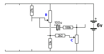
THE CAPACITOR
A long potentiometer indicates a high value of resistance. A short
potentiometer indicates a low value of resistance. When the circuit is
first turned ON:
The place to start is pot "C." Pots A and B are long and this
means they have a high resistance and thus there will be very little
voltage on the wiper of pot "C." Thus transistor C is not turned ON and
the LED is not illuminated.
This will make the wiper of pot B come down and pot B will shrink in
size. You have to remember pot B is a PNP transistor, so look up how it
is turned-ON.
This action is passed to pot C
and the third transistor is turned on quite a lot, but not sufficiently
to illuminate the LED.
Now we come to a feature you have never heard before. It is called SUPER
REGENERATION. Or FEEDBACK - positive feedback. Super Regeneration means
the circuit is driven into saturation.
The signal from the electret microphone has started a cycles that cannot
be stopped. We have included only those components that are involved in
this action.
The circuit also includes a feature: "time delay" or "delay" with the
100u and 100k and you can read about delays
HERE.
ASTABLE
MULTIVIBRATOR - How it changes state
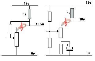
CONNECTING A LOAD
The value of the
components do not matter. The only thing we are going to
talk about is the effect of connecting a LOAD to the output of each stage and
the only component-value we need for the discussion is the value of the
collector resistor (10k).
Both circuits have been
designed to supply current through a 10k resistor to produce a voltage
of 6v across the collector resistor. When a 1k resistor is fitted, the
current required to produce 6v across it is 10 times more than before.
The transistor cannot do this and thus the voltage across the 1k will be
about 2v.
This arrangement is very bad. The output will be about 9v to 11.7v
The output of this arrangement is 1.5v to less than 1v and
is of no use AT ALL.
The second transistor will convert the 1k load into 100k according
to the gain of the transistor (this can be from 70 to 250) and the first
stage see the load as 100k and this does not upset the biasing of the
stage.
The
first thing to do is simplify the circuit to see how it operates.
Once you can see the top transistor is doing all the work you need to
see how the lower transistor detects the output voltage and feeds back a
signal to the emitter follower to maintain 5v.
The lower transistor can be replaced with a potentiometer. As the wiper
moves UP, the top transistor is pulled DOWN:
Why use a transistor to do this? Because the pot is not an
active component and cannot adjust itself to the changes in supply
voltage.
This arrangement is very sensitive because the lower transistor detects
1mV rise and this increases the current into the base by say 0.1mA and
it amplifies this current 200 times and effectively becomes a smaller
resistance and pulls the base of the upper transistor down to reduce the
output voltage by 1mV.
I design 100 analogue circuits for every common-emitter circuit.
Circuits that drive relays, motors, globes, speakers and LEDs. And yet
no University course has ever covered this type of circuit.
DANCING FLOWER
The electret microphone picks up a sound and when the output has a
negative excursion, the voltage on the base of the first transistor
reduces and the transistor turns OFF a small amount. This reduces the
current through the collector-emitter and this current is now diverted
to the base-emitter of the second transistor. The 2nd transistor turns
ON more and the collector-emitter reduces in resistance, so that the
voltage on the collector reduces.
No mathematics required and now you understand how the stage works.
If you don't follow my reasoning on SEEING A TRANSISTOR AS A
VARIABLE RESISTOR, how are you going to design the following type of circuit:
The transistor receives Infrared light from a LED and the resistance
between the collector and emitter leads reduces to a point where pin 5
of the microcontroller sees a low of less than 1.3v
The characteristics of the IR transistor are: 1M in darkness and
10k or less when detecting IR light.
But this circuit not very sensitive with the 10k collector resistor and the IR LED has to be very close
to the IR transistor for the microcontroller to register a LOW. .
How do you improve the sensitivity?
The IR transistor does not have a base lead, so all your theory about
biasing the base of a transistor is worthless. It does not apply. 
The IR transistor can on be turned on by the IR light and when it is
turned ON by very bright light, the resistance across the
collector-emitter leads is 10k.
The voltage divider becomes 10k in series with 10k and the voltage at
the join is 2.5v. This is not LOW enough for the
microcontroller to register a LOW and the circuit DOES NOT WORK.
If the 10k LOAD resistor is connected across the power rails, it will
pass twice the current. But if the LOAD resistor is connected to a
voltage that is HALF the 5v supply, it will take half the current. This
current is the same as the capability of the IR transistor and so, when
they are connected in series, they drop the same voltage across each
component. That's why the lowest voltage in the first circuit is 50% of
rail voltage or 2.5v.
If the IR transistor tries to "pull down" the 10k LOAD resistor, it will
want more current from the circuit and the IR transistor cannot pass
this extra current and so the two remain at 50%.
If the 10k LOAD is replaced by 100k LOAD, the current through the 100k
when connected across the power rails is a lot less than the capability
of the IR transistor and so the transistor will be able to "pull down"
the 100k until the current wanted by the 100k is equal to the capability
of the IR transistor. The transistor is capable of "pulling it down"
to almost the zero volt rail and we are not going into the exact value
but it is low enough for the microcontroller to detect a LOW.
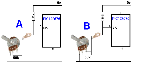
Here's how to see the circuit in operation:
For Circuit A: The 10k and 50k resistors form a voltage divider circuit
of 60k ohms. This puts about 1v across each 10k. 1v will appear
across the 10k resistor and pin5 will see a LOW of 4v. This is not
low enough for the microcontroller.
For Circuit B: The 100k and 50k resistors form a voltage divider circuit
of 150k ohms. This puts about 330mV across each 10k. The 100k will
have about 3v3 across it and pin5 will see a LOW of 1,700mV and this
will be low enough to trigger the microcontroller.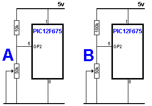
ooo0000ooo
Whenever you see a capacitor or electrolytic in a circuit that is NOT
connected to the positive or negative rail, it can perform unbelievable
magic tricks - like feedback and delays.
In the next two circuits you are going to see what they can do.
Now we will go back to the first circuit and explain how it works with
our "hand" and "potentiometer." No mathematics and no complexity.
Here is how the circuit works: The electret microphone picks up a
very faint sound and it produces an audio waveform. This consists of a
positive excursion and even less than 1mV will pass through the 100n
ceramic capacitor and activate the first transistor. This transistor
will have a gain of 100 or more and the current associated with the
input signal will be passed to the second transistor with an increase of
at least 100 times. The second transistor will increase the current by a
further 100 times and pass this signal to the third transistor.
The 3rd transistor will have the strength to illuminate the LED.
At the same time it will pull the negative lead of the 100u to the 0v
rail and via the 100k, the 100u will start to charge.
This charging current will take over from the signal from the microphone
and the circuit will stay in a condition of illuminating the LED.
The 100u will continue to charge for the next 20 seconds and when it is
nearly fully charged, the current will reduce to a point where the
second transistor is not activated. At this point the 3rd transistor
starts to turn OFF and then instantly the whole circuit turns OFF. The
100u puts a positive voltage on the base of the 2nd transistor that is
higher than 6v and the 100u gradually discharges for about 20 seconds
via the 27k, 100k and 10k resistors and then the circuit is ready to
detect a signal from the microphone.
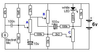
The electret mic deeds to produce a positive voltage to start the
circuit and this occurs when the
microphone turn-off a small amount and 47k is allowed to pass a positive
signal through the 100n capacitor. It only has to be a 1mV signal as
this will increase the current into pot A and it will shrink in size.
The bottom of the pot is connected to a 10u electrolytic and thus the
bottom of the pot will not move but the top will come down.
We can put the transistors back so you can see what is happening: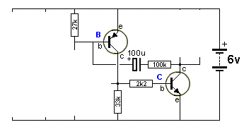
Transistor C has been turned ON a small amount and this has reduced the
voltage on the collector.
The reduced voltage on the collector is passed to the base of transistor
B via the 100k and 100u electrolytic.
This turns ON transistor B slightly more and the voltage on the
collector rises. This rise is passed to the base of transistor C to make
it turn on more. This action goes around and around hundreds of
times until transistor C is completely turned ON and the LED
illuminates.
During this time, the 100u has 100u electrolytic has not had time to
charge, but now it starts to charge via transistor C and the
emitter-base junction of transistor B.
It takes about 20 seconds to charge and when the it nearly fully
charged, the charging current reduces to almost zero. Transistor B
senses this zero base current and starts to turn off.
This reduces the base current for transistor C and the LED finally turns
off.
What have you learned.
Transistor A reduces resistance so more current flows in transistor B.
Transistor B reduces resistance so it can deliver more current to
transistor C.
Transistor C does not deliver any current. It just reduces
resistance so the 220R can pass more current and illuminate the LED.
Let's go over the operation of the circuit in another way.
The whole circuit operates on current. Each stage increases the current
about 100 to 200 times.
But each stage may not use all this current amplification. We don't know
how much is needed and we really don't need to know.
The electret mic will produce a waveform of 1mV to 20mV. We don't know
how much this waveform will increase the current into the base of the
first transistors, but let's say it is 0.1mA
The fist transistor is actually a common-emitter amplifier because the
emitter is fairly rigidly fixed to the 0v rail by the 10u capacitor.
This means it will shrink in resistance and allow an extra 0.1mA x 100 =
10mA to flow through the emitter-base connections of the second
transistor. This is already far more current than we need for the
operation of the circuit, but we will continue.
This current will be passed to the base of the third transistor and it
will be turned on. Maybe it gets turned on this quickly and the LED
illuminates.
The 100u will now start to charge and the charging current, through the
100k, will keep transistor 2 in a state of activation and produce the
FEEDBACK we covered above. It is only when the 100u gets fully
charged and the current drops to zero that the circuit turns OFF. The
100u will now begin to discharge via the 22k, 100k and 10k resistors.
THE MULTIVIBRATOR or FLIP FLIP or SQUARE-WAVE CIRCUIT
Now we come to a very popular circuit that has been covered hundreds of
times on the web.
But not once has anyone really covered how the circuit works.
It is a very complex circuit with a hidden feature that makes it so
reliable.
We have described the feedback effect in the circuit above that goes
around and around a few components and once it is started, it cannot be
stopped.
This feature also takes place in the FLIP FLOP Circuit and is the reason
why high current devices and globes can be connected to the circuit and
the circuit will always operate successfully.
This feature has never been mentioned because no-one is aware of its
contribution because no-one has added high current devices and
explained why the circuit works perfectly.
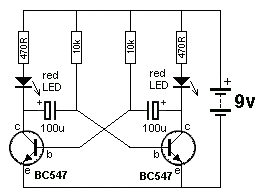
THE FLIP FLOP CIRCUIT
I have decided to explain how the Astable
(free-running) multivibrator changes state.
All the explanations on YouTube are vague and basically miss out the
most important parts of how the circuit changes state. This is because
the demonstrators don't really know how it works.
And I don't blame them, because it has NEVER been covered and they have
never built a circuit and tried to fix a fault.
All the videos talk about voltage levels and charging/discharging of the
capacitors and the state of each transistor. Some of this is correct and
some incorrect and some is over complex.
But how and why the circuit changes state has never been covered.
You need to know how the circuit works because when it fails to
oscillate, you need to know where to look.
The first omitted fact is this:
The two transistors do not operate like any other circuit, where the
transistor is turned ON just the right amount and then turned off.
In this circuit the transistor is turned on FULLY with up to 10 times
more base current than is required and then turned OFF and the other
transistor is turned ON with an "overdrive" This is one of the reasons
why this circuit is so effective and so reliable and will illuminate
LEDs as well as globes.
No-one has ever mentioned the fact that the transistors are turned on
FAR TOO MUCH but when you know this, you will have a much-better
understanding of how the circuit works. The enormously high current into
the base is delivered via the capacitors and when they are charging,
they appear as a resistor with a very small resistance and the high
current comes via the load resistor on the opposite side of the circuit
and the LED or globe.
The base resistors do not DRIVE the transistors. In other words, they do
not deliver BASE CURRENT to illuminate the LEDs. All they do is
discharge the capacitor and allow the voltage on the base to rise
sufficiently to START TO TURN THE TRANSISTOR ON. This takes no effect
(almost no current) and all it has to do is allow a small amount of
collector-emitter current to flow so that the voltage on the collector
is reduced slightly.
Now, let us explain how the transistors change state.
The first transistor has a negative voltage on the base and it is in
CUT-OFF mode where it is not conducting.
The second transistor has a voltage on the base and a current flowing
into the base because the capacitor on the base is charging. This
transistor is in SATURATION and the collector is at near 0v. (0.2v)
The negative voltage on the base of the first transistor is gradually
being removed by the base-bias resistor as it charges the capacitor
connected to the base. The voltage rises to the level of 0v and
increases to 0.55v and 0.6v. At the point the transistor starts to turn
ON but it does not take very much current to do so. This small amount of
current is supplied by the base-bias resistor.
When the first transistor turns ON, the collector voltage reduces
(falls) and the left lead of the capacitor is connected to the
collector. The voltage across the capacitor is irrelevant. The fact is
this: When the left-hand lead drops slightly, the right-hand lead drops
the same amount.
Now the voltage on the base of the right-hand transistor is very
critical as a transistor is not turned on AT ALL when the voltage is
0.5v but is fully turned ON when the voltage is 0.7v This is a range of
200mV and as the current into the base of the first transistor
increases, it is very easy for the voltage on the collector of the first
transistor to reduce by 100mV. This will reduce the voltage on the base
of the second transistor and turn it OFF slightly.
The voltage on the collector of the second transistor will rise slightly
and this increase will be passed through the capacitor to the base of
the first transistor.
This action goes around and around the two transistors (and two
capacitors) very quickly and is called REGENERATION.
Regeneration is: One action is amplified and passed to the second stage
in an increased form and this is passed to first stage as an increase
and finally the two stages change state.
This all takes place without the need for the two base-bias resistors.
The two capacitors act like two very low resistors and the
change-of-state takes place in a very heavily FORCED WAY. In other
words, the base current to the transistor being turned ON is very high
(it is much more than the transistor needs) and that's why the circuit
will drive filament lamps. In addition, this action is VERY FAST. It
has nothing to do with the value of the capacitors. They can be 1u or
100u and the action will be the same speed.
It is pointless describing the circuit in terns of voltages. The circuit
will work on any voltage from 3v to 12v and although the frequency will
change, the only thing you need to know is the act of Regeneration or
POSITIVE FEEDBACK and the two states that are held for a long period of
time are: one is in COMPLETE CUT-OFF and the other is heavily
SATURATED.
When you connect a LOAD to a transistor stage, the voltages
on the stage will change. That's why you cannot design a stage without
knowing the characteristics of the input device and the resistance of
the LOAD.
An output device (LOAD) may be a relay, motor or globe having a
resistance of 50 ohms to 1k.
We are going to show how to connect it.
Here are two common-emitter stages that have been designed to have
half-rail voltage on the collector. It doesn't matter if it a self
biased stage or H-bridge design. The two circuits are basically the
same.
A self-biased stage and H-Bridge
We have a 1k LOAD and it can be connected 3 different ways.
The transistor is a pot that tries to pull the 1k down
This means the output voltage will range from about 8v to 11.5v
instead of the previous 3v to 11.5v
These are just approximate values to show the output will be reduced in
amplitude.
The second way to connect the 1k LOAD is across the 10k: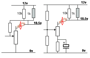
The pot tries to pull the 0.9k down
The 3rd way to connect the 1k LOAD: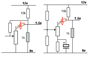
The 1k just about kills the output
Now we are going to show how to add the 1k LOAD via an emitter-follower
stage (also called common-collector):
This is called IMPEDANCE MATCHING or BUFFERING or LOAD MATCHING or
INTERFACING.
The emitter-follower converts the 1k into 100k
The waveform on the 10k collector resistor will now be transferred to
the 1k LOAD and now you will get the same amplitude across a lower value
of resistance.
The second transistor is an emitter-follower. What does an
emitter-follower do? It converts the LOAD into a HIGH RESISTANCE. It
increases the resistance about 100 times and this corresponds to the
gain of the transistor. The increase can be from 70 times to 250
times.
About the only thing Universities describe is a transistor amplifier.
But transistor amplifier are the last thing you come across as an
electronics design engineer. Most of the circuits are called
"interfacing circuits or power supply circuits and these have never been
covered - because the "professors" don't have a clue.
Here is a simple 5v power supply that can be used with old batteries to
get the remaining energy from each cell.
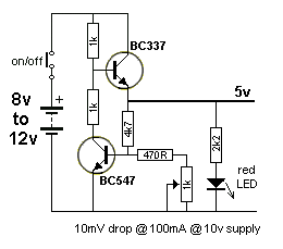
It can be simplified to a emitter-follower stage made up of the BC337.
The voltage on the base is adjusted so that it is about 5.7v and the
output is 5v.
This is a very poor way to set the output voltage because the input
voltage will fall when a current is flowing and the base voltage will
drop (droop). 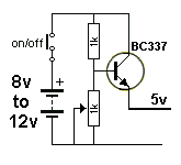
Now we look at the two transistors:|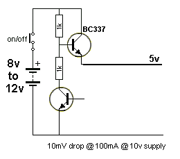
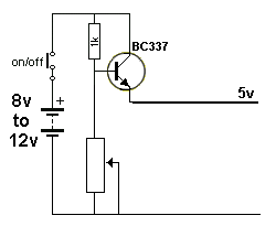
This is how the lower transistor pulls the top transistor down.
The 1k base resistor allows the transistor to rise when we reduce the
"pull DOWN." The circuit only pulls the BC337 DOWN.
The 1k pulls it UP.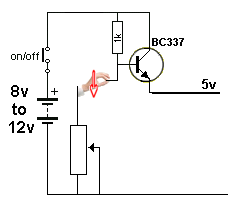
The lower transistor monitors the output voltage and changes its
resistance to maintain the 5v.
How does it do this?
The lower transistor is effectively connected to the 5v output. When the
5v rises, the pot reduces in resistance and this pulls the BC337
transistor DOWN. It's called a FEEDBACK CIRCUIT. 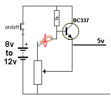
or STABILIZING Loop
It is the amplifying capability of the lower transistor that allows a
very small change (and thus a very small change in current) Into the
base to be passed to the upper transistor to produce a firm grip on the
base. It can only have a pulling DOWN effect on the base and it is
acting against the 1k resistor. When it reduces its "grip" the 1k pulls
the BC337 UP. This is called a NEGATIVE FEEDBACK loop or STABILIZING Loop.
You can have POSITIVE FEEDBACK to increase the output of a circuit or
NEGATIVE FEEDBACK to reduce or "counter" the effect.
All the changes in voltage are converted to current changes as the
transistors only respond to CURRENT CHANGES.
This is something that has never been explained in any lecture.
You don't need any mathematics and you cannot use any mathematics
because you don't know the gain (amplification factor) of any of the
transistors. This value changes according to the current and no
two transistor have the same value.

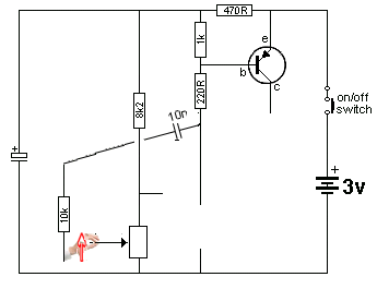
This circuit comes from a toy Dancing Flower. The stem is hollow and a
bent shaft comes from the motor in the base to make the flower wiggle
when you tap the pot or whistle.
There are 3 important hidden features in this circuit that we will
cover.
The first is the need to prevent the noise from the motor traveling
along the power rail to the front-end and upsetting the electret
microphone. That's the purpose of the 470R and 10u electrolytic. They
are smoothing components.
The second is the need to turn ON the motor with a high current
capability as a motor wants about six times the operating current to start
turning. This is provided by the PNP transistor and the 220R on the
base.
And the 3rd feature is the operation of the 10n capacitor. It provides a
delay to keep the motor operating for a few seconds after a noise is
detected. And that's what we are going to explain. 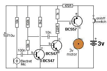
Two components are connected to the collector, with one of them being a
220R resistor.
Current through the 220R will increase and this increased-current will
also flow through the emitter-base leads of the third transistor.
Each transistor increases the current by a factor of about 100 to 250,
so that a very tiny current produced by electret microphone is
amplified: 200 x 200 x 50 times. It is eventually capable of
driving a motor.
Here is a point to note: Even though the electret microphone
produces a signal in the positive and negative direction, only the
negative direction is detected and amplified by the circuit. And it is
this reduction of current by as little as 0.01mA that will activate the
circuit.
The circuit we are talking about NOW is called a FEEDBACK circuit and consists of the two transistor and components
shown below. When this section is activated by a slight reduction in
current on the first transistor - NOTHING WILL STOP IT.
But this effect is not able to really turn the motor ON. It just give a
very short pulse to the motor.
The real component in this design is the 10n. It does all the magic.
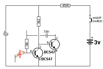
A slight decrease on the base current
of the first transistor
will make the 8k2
pull the base of the
second transistor UP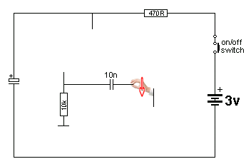
and turn on the transistor.
This will pull the
10n DOWN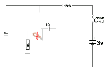
and the other lead of the 10n
will go DOWN too and this 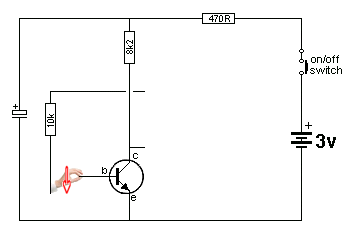
will pull the base of the first transistor down
MUCH MORE than the tiny "pull down"
from the electret microphone.
The 10n does two things. Firstly it provides a feedback
signal and then it provides a DELAY to keep the motor activated.
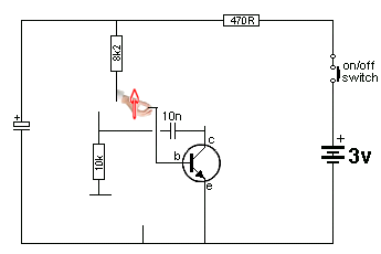
Going over the
action again:
When the voltage on the collector of the second transistor drops, the right-hand lead of the 10n
falls and because the 10n is not charged, the left-hand lead falls too.
The 10n acts like a direct link from one lead to the other.
It might fall by more than 1v. Previously, the voltage on the top
of the 10k will be slightly higher than 0.8v and now it falls by 1v.
This immediately removes the 0.7v "turn-ON" voltage on the base of the
first transistor and completely takes over from the tiny effect of the
electret microphone.
The circuit is now fully activated and the motor operates at full speed.

The circuit stays in this condition for a few seconds while the 10n
charges via the 820k. When the voltage on the join of the 10k and 820k
reaches 0.8v, the first transistor turns ON and this turns the rest of
the circuit OFF.
The microphone sits and waits for the next whistle but it cannot
activate the circuit while the 10n starts to charge in the opposite
direction as the right-hand lead is very close to 3v and the charging
current will keep the first transistor OFF during this time.
When the voltage on the base of the first transistor is below 0.5v (and
can be negative), the resistance of the base is infinite and that means
the bottom of the 10k goes "nowhere." The 10n is not affected by
the 10k. The 10k puts a low voltage on the base of the transistor and
the transistor is turned OFF completely.
The 10n gets charged via the 820k and this takes a long time. As soon as
the voltage on the base of the transistor rises above 0.55v, the
transistor starts to turn ON.
As soon as the first transistor starts to get turned ON, the whole
circuit changes state.
The first transistor becomes a very low resistance and this turns OFF
the second transistor and the second transistor disappears from the
circuit.
The 10n now gets pulled HIGH by the 220R and emitter-base junction of
the third transistor and the high charging current keeps the circuit in
this condition for a short period of time until the 10n is charged.
And then the 820k takes over to keep the transistor turned ON with the
slightest amount of current, so that a signal from the electret mic can
over-power this effect and start the cycle again.
I have covered a lot of features in this cycle and you have to
understand it is the CURRENT that is present in each part of the cycle
that is: "doing the work."
Not once have I mentioned the 0.7v base-emitter voltage as this doesn't
have to be talked about to understand how the circuit operates.
It is the amplifying - or increasing - in CURRENT - that is the
function of the circuit. We only have 3v supply but the current has to
be increased more than 100,000 times (from the output of the electret
mic) to operate the motor. That's why you need 3 transistors. And
a motor needs 3 to 6 times extra current to start it revolving.
That's why you need the extra current "up your sleeve."
A transistor increases the current in one of two ways. It can either
decrease in resistance or have a lower
value of LOAD resistor and and this LOAD resistor delivers a higher
current to the next stage.
And the 3rd transistor decreases its resistance enormously so the motor will operate. For the
transistor to do this the second transistor has to be able to reduce in
resistance and this is achieved via the 8k2 LOAD resistor on the
collector of the first transistor.
In the quiescent state (rest state, resting state, waiting state)
the first transistor is turned ON slightly so only a small (extra) signal
from the microphone will activate the circuit.
We cannot provide an accurate amount of "turn-ON" but the 820k will be
converted to 4k2 via the first transistor if the gain of the transistor
is 200. (We will - or have - covered this in another articles and
a link will be provided when the link is found).
This will bring the collector voltage down to 1v if the second
transistor is not connected and we can see this is not below 0.7v for
the second transistor to turn ON.
So the biasing does not affect the circuit and a small amount of
assistance from the microphone will activate the circuit.
There are a lot of concepts that have been covered in this explanation
that have never been covered in any lecture or text book because they
are visual identifications and pertain to how I "see" a circuit working in my mind.
If you don't use these concepts you would never realise how important
the 10n is. It changes the whole operation of the circuit.
Here are 4 of the "concepts:"
The circuit is turned on slightly via the 820k so the microphone detects
the slightest sound.
The 10n takes over from the microphone signal
The 10n produces a delay.
The direct coupling of the 3 transistors produces an enormous
amplification.
You need enormous amplification to activate the motor.
HOW DOES A TRANSISTOR WORK?
Now that you have read how the circuit above works, we will cover the
operation of the second transistor.
You have to learn electronics "in reverse." You need to have a
problem and learn how to solve it. That's the only way you remember.
I remember every fault I fixed in electronics equipment over the past 50
years. That's because I may come across it again.
But Universities don't teach like this and that's why they are a
failure.
When (if) the first transistor turns OFF, the 8k2 will pull the base of
the second transistor HIGH.
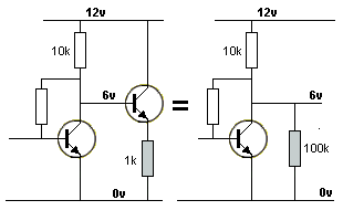
Here is a feature you have to remember: The 2nd transistor will reduce
the 8k2 to 41 ohms if the transistor has a gain of 200. This is
because the value will be: 8,200/200 = 41 ohms
This is a very small value and the circuit does not need all this amount
of reduction (amplification) - but that's what the transistor is capable
of doing.
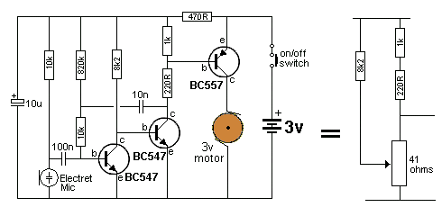
to turn into a 41 ohm resistor
The low resistance allows a high current to
flow in the emitter-base junction of the BC557 transistor
and it also helps you work out how much current will flow.
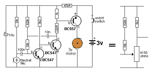
And the same reasoning (feature) applies to the first transistor. It converts the 830k into 4,150 ohms (830,000/200 = 4,150 ohms.
It turns the stage into a simple voltage divider.
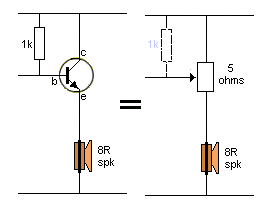
The transistor can "pull" the top of the speaker UP with a force equal
to a 5 ohm resistor, if the gain of the transistor is 200. This can
effectively put mid rail voltage across the speaker. A signal on the
base will increase and decrease this voltage.
We have learnt that increasing the current to the base reduces the
resistance of the transistor.
There is nothing "magic" about the circuit. A positive input signal
changes the input transistor from a HIGH resistance to a LOW resistance.
This, combined with the 470R increases the emitter-base current of Q2 to
activate the amplifier.
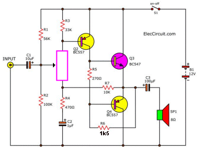
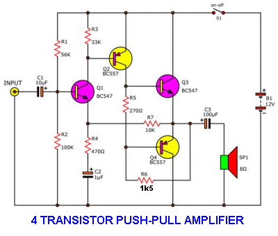
PUSH-PULL OUTPUT
The image above is an animation with each frame giving 4 seconds
viewing. It shows how the components in the circuit disappear when not
required and how the 100u actually goes below 0v rail to deliver its
energy to the speaker to make the cone move in the opposite direction to
complete the second half of each cycle.
All we are showing is: how to view the effect of the 1k (via the
transistor) on the speaker. You don't need any mathematics or equations.
Just a simple conversion.
This concept only applies to the circuits above and is a quick way to
determine the capability of a stage.
For the third transistor in the circuit above, you need a different approach. The
emitter-base current is 3/260 = 11mA. The transistor can deliver
150 times this current via the emitter-collector terminals = 1650mA and
this is more than sufficient to operate the motor. Obviously this high current
will not be flowing due to the resistance of the motor, but we need
to know if the circuit will deliver sufficient current to start the motor
revolving.
All this understanding is much more important than working out the
mid-rail voltage of a common emitter stage or being indoctrinated into
the multitude of mathematical equations of an H-Bridge design as shown
in so many University lectures and YouTube videos.
Most of your work will revolve around INTERFACING and this can be
front-end designs or LOAD designs.
Sometimes you will need to design a direct-coupled circuit and this will
involve added challenges as the gain of each stage will make quiescent
conditions a difficult thing to achieve.
These are the topics we will cover in another discussion.
Some of the things we have covered can be applied to the following
circuit to see the major mistake.
Take Q3. Its base is "pulled HIGH" by the action of Q2. This can be a
very strong "pulling force."
With Q4 the force on the base is via a 1k5 resistor and this will not be
as strong. This means the Push-Pull action of the amplifier will not
equal.
Next we have to work out if the 10k feedback resistor is producing
positive or negative feedback.
When the input rises, Q1 rises too as it is basically an emitter
follower. All the increase in voltage appears across the 470R and any
increase in current is detected by Q2. This is a very poor transfer of
signal and is another point of poor design.
However if we follow the signal-path we see Q2 turning ON, raising the
position of Q3 as an emitter-follower and raising the voltage on the
right lead of the 10k feedback resistor.
This will have an effect of raising the voltage on the emitter of Q1,
thus turning it OFF and reducing the effect of the input signal.
Thus the 10k is a NEGATIVE FEEDBACK component and controls the stability
of the circuit.
You would need to test the circuit with an oscilloscope to see what
amplitude input signal is needed to obtain a worthwhile output.
It is not known how much of the input signal is passed to the amplifier
as most of it is lost in the 470R resistor.
Effectively, Q2 is being PULLED DOWN by a 470R resistor as we can remove
Q1 and perform this equivalent. There will be some losses due to the
voltage developed across the 470R resistor but these will be small.
Only about 5% of the active feedback from the 10k is fed to the first
transistor but the 10k has an impact on setting the operating point as
it adjusts the voltage on the emitter by charging the 1u via the 470R
resistor. The 1u is "fixed rigid" as far as the AC signal is
concerned.
The input transistor is initially a HIGH RESISTANCE
A positive signal on the input turns the transistor into a very SMALL
resistance
As soon as you change transistors into variable resistors, you will
start to understand how circuits work.
Everyone thinks the electrolytic on the output just prevents DC from
entering the voice coil of the speakers. But it does much more than
this.
I mentioned above that you need to pay particular attention to
capacitors contained within the body of a circuit and this is a typical
example.
The 100u is the secret to the circuit working. Without it, the circuit
would not work. And if the value is too small or too large, the circuit
will fail.
Here is an animation of the function of the 100u electrolytic:
Wait for the
animation to cycle and re-start
It delivers a negative voltage to the speaker and it has to be
charged as much as possible to do this.
We mentioned a feature that has never been covered.
Q4 is capable of pulling the 100u DOWN. When a signal from the 270R is
removed, the base sees a voltage from the 100u. It will be about
6v maximum and via the 1k5, the base gets a current to turn the
transistor ON. It's a bit like pulling yourself Up by your shoe-laces,
but in this case it works.
The transistor turns its self ON and lowers the positive lead of the
100u. The negative also gets lowered. This is called a FEEDBACK
arrangement because when it starts, it continues. It can also be called
a form of BOOTSTRAPPING where the voltage increases due to a positive
feedback.
This is a very difficult concept to visualise, but when the 100u is
pulled UP, current flows UP through the speaker. When the positive lead
of the 100u is pulled down, current flows DOWN through the speaker.
There is no voltage across the speaker at the moment, so when the
transistor turn ON, the negative lead will immediately go to minus 6v
and the top of the speaker will be 6v NEGATIVE.
If the top of the is 6v negative, the bottom of the speaker is 0v. The
positive lead of the 100u will push current through the voice coil from
the top of the speaker to the bottom and thus the current will flow
DOWN.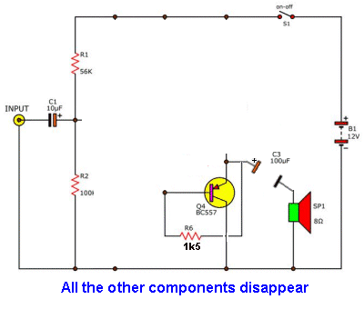
with your boot-laces.
The effect and operation of the 100u and Q4 has never been discussed in
any text book or lecture, but they form an important part of
understanding how a circuit REALLY works.
Here is an animation of how the current flows in an ammeter as the
electrolytic is charged and discharged. We say the current reverses
direction and the voltage will also reverse direction during the
charging and discharging. The initial charging and discharging produces a maximum
current and it gradually tapers off to zero when the capacitor is fully
charged or discharged. The polarity of the voltage changes also but this
is not evident on the animation, so a further animation is provided.
Here is an explanation of the effect of the electrolytic on energising
the speaker.
The 4 frames:
1. The electrolytic sits above the speaker, fully charged.
2. The transistor connects the positive lead of the capacitor to the 0v
rail.
3. The capacitor immediately falls to below the 0v rail as shown in the
animation.
4. We can "swing" the capacitor to a position above the 0v rail and see
the negative lead is connected to the speaker.
That's how the speaker gets a negative voltage to move the cone in the
opposite direction.
If the speaker is replaced with a motor, it will revolve clockwise and
anticlockwise to prove this.
BOOTSTRAPPING
There is no gain from the output of the circuit, through the 100u, so
the only reasoning is the increased voltage across the 1k8 is allowing
the transistor to turn off more and increase the 6v.
This circuit shows the amazing effect of adding a capacitor to random
locations and detecting the result.
ooooo00000ooooo
Here is an example of poor design. The output might sound
impressive but when you look at the value of the components you will see
the output will only be a fraction of the potential wattage.
We will just consider the components surrounding the top output transistor:
We have 14.7 ohms in series with 8 ohms and this will deliver about 30%
of rail voltage to the speaker.
The 10k base resistor on the top transistor will convert to 100 ohms (if
the gain of the transistor is 100 . . . 10,000/100=100) and the load will see 30% of rail
voltage (using voltage divider law). If the transistor can produce a gain of 200, the load will see
50% of rail voltage.
ooo000ooo
Look at this circuit. There is NO VOLTAGE for the negative half cycle
!!!
In this circuit we see the effect of a 100u electrolytic producing an
increased output on a stage due to a FEEDBACK effect and the result is
called BOOTSTRAPPING.
Our test circuit increased a 100mV input signal to over 2v and the
effect was especially noted when the input signal was a low value.
The circuit worked with a 1M into the circuit with 1v signal. The
circuit also worked with 1u Bootstrap electrolytic. 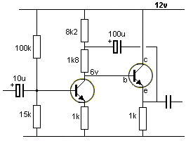
When the audio frequency is below 200Hz, the 250u electrolytic will
charge fully. But when the frequency is about 2,000 Hz, the electrolytic
will charge to about 10%. This is because the capacitor does not have
time to charge before the signal changes to the second half of each
cycle.
These are things that have not been taken into account when designing
the circuit.
Here is another example from YouTube. You see how badly it has
been designed:
The RC time-constant for 50 ohms, 100u and 50 ohms is 0.01second and
this means the capacitor will charge fully with a signal of 100Hz or
less. When the signal is about 1k, it will only charge to a
very small amount and this is the energy that will be supplied to the
load on the second half of the cycle, via the lower transistor.
Now you know what to look for in a push-pull arrangement, you can see
this circuit will NOT deliver.
And now another Push-Pull amplifier with the same problem.
Designers think a large output capacitor will transfer more signal. But
that is not the case. It has to be DESIGNED for the circuit. The energy
stored in the capacitor on the first half of the cycle is delivered on
the second half. But the capacitor has to small enough to charge to a
high VOLTAGE and a large capacitor will take a long time to charge - but
the frequency does not allow enough time.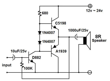
The electrolytic is too big!!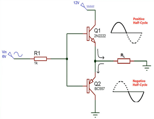
You can't put just anything in a text book !!
Q4 is connected incorrectly. You must know a little bit about
electronics before you put a circuit on YouTube.
oooo0000oooo
BASE-EMITTER VOLTAGE
ARROWS
ooo000ooo
Another 100 Transistor Circuits can be found
HERE.
Go to
Talking Electronics
website
5/3/2024
How does Q4 work????
It doesn't matter what you hear from these amplifiers. You may think the
output is clean, but circuit analysis will show otherwise. We are covering
the technical faults in the design. You cannot detect distortion below
10% and you don't know what miss-match needs to be present to produce
this 10%. Some music will highlight the distortion while other
"thumping" music will hide the distortion.
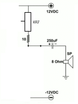
THE OUTPUT ELECTROLYTIC
The output consists of a resistor and capacitor. The resistor can be the
resistance of the transistor plus the resistance of the speaker.
A resistor and capacitor in series is called an RC CIRCUIT and it
has a certain time to charge and a time to discharge. This is called the
RC Time and it is not the time for the capacitor to fully charge
but to charge to 63%. This value has the Greek letter Tau. And we say
the circuit has a TIME CONSTANT of ONE (for 63%). The charging of
a capacitor is not linear and after a period of two Time Constants the
capacitor will charge to 86% and then 95%.
In the circuit above with the C5198 transistor and 680R base resistor,
8R speaker and 1,000u electrolytic, the Time Constant is 0.015seconds.
This means a frequency of 33Hz will take 0.015 seconds to charge the
capacitor to 63%. Any frequency above 33Hz will charge it to a lower
value.
At 33Hz the capacitor will charge to 63% and this is the
energy the circuit will pass to the speaker on the second half of the
cycle. You can see the frequency is very low and effective transfer of
energy is very small. That's why you need to make some simple
calculations before publishing a circuit.
I have not mentioned the base-emitter voltage in any of my discussions
because it is so small that it does not come into any of the
calculations.
All you have to remember is this: A transistor does not turn ON
with a base-emitter voltage 0.5v - or less. At 0.55v, it starts
to turn ON and as you deliver more current to the base, the base-emitter
voltage rises to 0.6v, 0.65v, and even 0.7v.
Some transistors have a slightly higher voltage, but overall this
voltage is not important and measuring it does not
tell you very much. You can also put minus 5v to
minus 6v on the base but any higher voltage will cause a very high current to
flow as the junction will starts to break-down (reverse break-down).
Do not worry about the base-emitter voltage as there are many other
features you need to understand when designing a circuit, so concentrate
on the important details.
Things like current through a transistor, the heating of a transistor,
its gain, maximum voltage and cost.
I have used BC547 for NPN transistors in all my diagrams as it means the transistor is a
general purpose type with no special features and BC557 for PNP types,
both of which can pass up to 100mA MAX. BC338 means the collector
current can be as high as 1 amp, but I would not recommend anything
higher than 300mA. These are all good for 25v circuits.
Any other type of transistor has been used for a special purpose.
That's how you quickly identify a circuit and what to expect.
PNP TRANSISTORS
I have not covered PNP transistor stages because the biasing can be
difficult if the supply voltage reduces when a load is activated. You
have to see a circuit that uses both NPN and PNP transistors and see how
the circuit can be designed around a PNP transistor with almost zero
effect on the biasing.
PNP and NPN transistors have almost exactly the same characteristics and
features and there is no need to worry about reduced capabilities.
I don't like arrows on a circuit diagram. I don't know if they mean
energy is being sent OUT the lead or energy is entering. I don't
know if -Vcc is a negative voltage or another 0v rail.
0v rail means a number of things and it refers to GROUND, EARTH, CHASSIS
or zero volts.
It also means the negative terminal of say a car battery. For
mains wiring it is the NEUTRAL wire. Neutral is not the same as earth in
electrical wiring. Even though both can have zero volts on them, The
Active, Neutral and Earth are kept separate so that
Earth-Leakage-Detectors can detect 15mA difference in the current
flowing through the Active and Neutral wires and 'trip" the circuit. 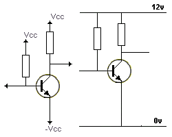
I have been teaching electronics for over 50 years with 750,000 books
and magazines and over 25,000,000 viewers to my website. I have
never used an equation for any of my teachings or any the 350 projects
and modules.
It's wonderful to understand how to calculate things to the nth degree
but none of this is necessary.
Not one student in 50 years has contacted me to say they failed to get
employed because they did not know Thevenin's Theorem. And I have never
been asked to produce an article using equations. I aim to get you to
understand how a circuit works and not get "tied down" with
complications. You can see by the comments on YouTube that not a single
student understands a single bit of the discussion. All they say:
"Wonderful explanation!" So is explaining the operation of the
cyclotron, wonderful !
MESMERISM
Students are being mesmerized and bamboozled with University lecturers
that explain nothing about understanding how a circuit works and how to
design a circuit.
All the lectures are based around being able to produce an answer to a
mathematical problem.
That's not how electronics works.
None of the simple explanations above have used mathematics. None are
ever contained in any University curriculum because the answer requires
intelligence and understanding and that is foreign to a lecturer who has
never designed a circuit in his life.
More enlightening discussions and concepts can be found
HERE.
https://www.talkingelectronics.com/projects/TheTransistorAmplifier/TheTrAmp/TheTrAmpP1.html
More on the Transistor Amplifier can be found
HERE.
https://www.talkingelectronics.com/projects/TheTransistorAmplifier/TheTransistorAmplifier-P1.html
100 Transistor Circuits can be found
HERE.
https://www.talkingelectronics.com/projects/200TrCcts/200TrCcts.html
https://www.talkingelectronics.com/projects/200TrCcts/101-200TrCcts.html
After you read and study and understand what I have produced, you will
be able to design many types of circuits. These are called
BUILDING BLOCKS and by connecting blocks together you create circuits
that do magical things.
Contact Colin
Mitchell if you want any help
Let me know if I have missed a spelling mistake or forgotten something.
I am proof-reading things all the time and this has reached more than 10
revisions. It takes an enormous amount of brain-power to write technical
explanations and that's why no-one has gone into the depths of
describing the technicalities of circuit-design.24-2-2024