This huge article is all
about a
simple explanation of how a transistor works in a circuit, and how to
connect transistors to create a number of different circuits. No mathematics and no complex wording.
Just a
completely different approach you can understand . . .
Just before you go to the article below, I want to mention
another article I have produced in response to the terrible
YouTube videos.
I have finally outlined how I see a circuit working "in my
mind" and the truth is this: everything I have
mentioned and everything you have read, and seen and been
told is INCORRECT. I see a transistor as a
variable resistor and all circuits work on the simple
concept of VOLTAGE DIVISION.
You can see this article and the 5 pages I have written
HERE. And
you have to combine all these facts so you can also see a
CIRCUIT WORKING.
(Note: The .pdf is old and out of date).
Dear Sir,
I would like to thank you for explaining
electronics in such a simple and wonderful way.
I have read so many textbooks on transistors and
transistor circuits, but only after reading
your Transistor Amplifier e-book and making
some of the circuits have I really understood
how a transistor works.
I am not saying mathematics of a transistor is
unimportant. I am saying a transistor
should be introduced exactly the way you do it.
Many thanks once again.
Best regards,
Ante Kotromanovic
I have produced a separate
article on HOW THE TRANSISTOR WORKS and it covers a lot of
aspects of the COMMON EMITTER AMPLIFIER. Click
HERE
My latest article explains
how I see a transistor circuit working "in my mind" and you
will realise everything you have heard, read, and seen is
totally FALSE. It will be the most "eye-opening" discussion
you will ever read. . . .and the most educational.
Click
HERE
This eBook starts by
turning
ON a single transistor with your finger
(between two leads) and
progresses to describing how a transistor can be connected to the supply
rails in 3 different ways.
Then it connects two transistors together DIRECTLY or via a capacitor to produce
amplifiers and oscillators.
As you work through the circuits, the arrangement of the parts are
changed slightly to produce an entirely different circuit with new
features.
This way you gradually progress through a whole range of circuits (with
names you can remember) and they are described as if the parts are
"moving up and down" or "turning on and off."
Even some of the most complex circuits are described in a way you can
see them working and once you get an understanding, you can pick up a
text book and slog though the mathematics.
But before you reach for a text book, you should build at least 50
circuits . . . otherwise you are wasting your time.
I understand how the
circuits work, because I built them. Not by reading a text book!
From a reader, Mr Ashvini Vishvakarma,
India.
I was never taught the influence of the coupling capacitor in
capacitor-coupled single transistor stages.
No one told me that RL of one stage delivers
the input current of the next stage.
No text book has ever mentioned these
things
before because the writers have never built any of the
circuits they are describing. They just copy one-another.
That's why this eBook is so informative. It will teach
you things, never covered before.
I don't talk about "formulae" or produce graphs because
transistors have a wide range of parameters - especially the
gain - and this has the greatest effect on the operation of
a circuit. It is faster to build a circuit and test a
transistor than work out the "Q-point" from a load-line.
The same with two resistors in parallel. It is faster to put
them together and measure the resistance, than look up a
nomograph.
You learn 10 times faster with actual circuits than
theoretical models and 10 times smarter when you know how to
avoid mistakes.
Dear Colin,
After many attempts to grasp transistor biasing,
I did not get it until I eventually found your tutorial
on it! You put it so clearly and straight forward.
Best of all, you actually demonstrate with numerous
examples, step by step!
What a joy, to learn from your tutorial!
Thank you for this excellent article!
Kind regards
Jörg Rauh
This discussion
gets 300 visitors a day. That might not sound
much but it has recorded 310,000 readers to date.
I have not included one complex word or formulae.
I have described everything so you can eventually
"see" a circuit working in your mind and once you
know all the technical requirements, you will be
able to see why it does not work.
- Colin
9-6-2016
Here is
Electronics
I
course from South
Dakota School of Electronics. These links do not work as of 2-3-2024
These lectures cover the mathematical side of how
various circuits work.
Once you complete this eBook, the lecture notes will be
much easier to understand.
My interpretation of
the above-course is this:
It goes into far too much detail and far too much
mathematics.
There is very little on digital concepts and nothing on
microcontrollers.
Time would be much better spent on explaining transistor
and MOSFET behaviour in a simpler way and getting on
with digital circuitry and microcontroller projects. The
student should build at least 20 projects for the year
as this is the only REAL way to learn. I give the course
2/10. It really is a WASTED year.
You simply cannot put a transistor into a circuit and
expect it to produce the calculated results. The gain of
a transistor can be from 100 to 200 in a batch and this
changes the outcome by 50%!!
Instead of taking 30 minutes to work out the answer,
simply build the circuit and measure the REAL result.
Let's Start:
THE TRANSISTOR
How to remember:
NPN (Never Points iN), PNP (Points iN Permanently)
THE NPN TRANSISTOR
There are thousands of transistors and hundreds of
different makes, styles and sizes of this amazing device. But there are only two different
types. NPN and PNP. The most common is NPN and we will cover it first.
There are many different styles but we will use the
smallest and cheapest. It is called a GENERAL PURPOSE TRANSISTOR.
The type-numbers on the transistor
will change according to the country where it was made or sold but
the actual capabilities are the
SAME.
We are talking about the "common" or "ordinary" or
original type.
It is also referred to as a BJT (Bi-polar Junction
Transistor) to identify it from all the other types of
transistors (such Field Effect, Uni-junction, SCR,) but
we will just call it a TRANSISTOR.
Fig 1. NPN Transistor
Fig 1 shows an NPN
transistor with the legs covering the symbol showing the name for each
lead.
The leads are BASE, COLLECTOR and EMITTER.
The transistor shown in the photo has a metal case with a tiny tag
next to the emitter lead.
Most small transistors have a plastic case and the leads are in a
single line. The side of the transistor has a "front" or "face" with
markings such as transistor-type.
Three types of transistors are shown below:
Fig 1a.
Fig 2. NPN Transistor
Symbol
Fig 2 shows two "general purpose" transistors
with different pinouts. You need to refer to data sheets or test the
transistor to find the pinout for the device you are using as there are
about 5 different pin-outs.
The symbol for an NPN transistor has the arrow on the emitter
pointing AWAY from the BASE.
Fig 3. NPN
"Water Valve"
Fig 3 shows the equivalent of an
NPN transistor as a water
valve. As more current (water) enters the base, more water flows from
the collector to the emitter. When no water enters the base, no water
flows through the collector-emitter path.
Fig 4. NPN
connected to the power rails
Fig 4 shows an
NPN transistor connected to the power rails.
The collector connects to a resistor called a LOAD RESISTOR and the
emitter
connects to the 0v rail or "earth" or "ground."
It can also be called the negative rail.
The base is the input lead and the collector is the output.
The transistor-type BC547 means a general-purpose
transistor.
Sometimes a general-purpose transistor is called TUN - for
Transistor Universal NPN.
A general-purpose PNP transistor is called TUP - for
Transistor Universal PNP.
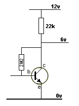
Fig 5. NPN Transistor biased with a
"base bias" resistor and a LOAD resistor
Fig 5 shows
an NPN transistor in SELF BIAS mode. This is
called a COMMON EMITTER stage and the resistance of the BASE BIAS
RESISTOR is selected so the voltage on the collector is half-rail
voltage. In this case it is 2.5v.
To keep the theory simple, here's how you do it. Use 22k as the load
resistor.
Select the base bias resistor until the measured voltage on the
collector is 2.5v. The base bias resistor will be about 2M2. This is how the transistor gets turned on by the base bias resistor:
The base bias resistor feeds a small current into the base and this
makes the transistor turn ON and creates a current-flow though the
collector-emitter leads.
This causes the same current to flow through the load resistor and a
voltage-drop is created across this resistor. This lowers the voltage on
the collector.
The lower voltage causes a lower current to flow into the base, via the
base-bias resistor, and the transistor stops turning on a slight amount.
The transistor very quickly settles to allowing a certain current
to flow through the collector-emitter and produce a voltage at the
collector that is just sufficient to allow the right amount of current
to enter the base. That's why it is called SELF BIAS.
Fig 6. Turning
ON an NPN transistor
Fig 6 shows the transistor being turned on via a finger.
Press hard on the two wires and the LED will illuminate brighter. As you
press harder, the resistance of your finger decreases. This allows more
current to flow into the base and the transistor turns on harder.
Fig 7. Two transistors turning ON
Fig 7 shows a second transistor to "amplify the effect of
your finger" and the LED illuminates about 100 times brighter.
Fig 8. Adding a capacitor
Fig 8 shows the effect of putting a capacitor on the base
lead. The capacitor must be uncharged and when you apply pressure, the
LED will flash brightly then go off. This is because the capacitor gets
charged when you touch the wires. As soon as it is charged, NO MORE
CURRENT flows though it. The first transistor stops receiving current
and the circuit does not keep the LED illuminated. To get the circuit to
work again, the capacitor must be discharged. This is a simple concept
of how a capacitor works. A large-value capacitor will keep the LED
illuminated for a longer period of time as it will take longer to
charge.
Fig 9.
Adding a capacitor to the
output
Fig 9
shows the effect of putting a capacitor on the
output. It must be uncharged for this effect to work. We know from
Fig 7 that the circuit will stay ON constantly when the wires are
touched but when a capacitor is placed in the OUTPUT, it gets charged
when the circuit turns ON and only allows the LED to flash.
The
electrolytic must be manually
discharged to see the effect again.
1.
This is a simple explanation of how a transistor works.
It amplifies the current entering the base (about
100 times) and the higher current flowing through the
collector-emitter leads will illuminate a LED or
drive other devices.
2.
A capacitor allows current to flow through it until it
gets charged. It must be discharged to see the
effect again.
TRANSISTOR PINOUTS:
Transistor Pinouts
Just some of the pinouts for a
transistor. You need to refer to a data sheet or test the device to
determine the pins as there are NO standard pin-outs.
THE RESISTOR
Before we go any further, we need to talk about the RESISTOR.
It's a two-leaded electrical component that has resistance from a
fraction of an OHM to many millions of ohms (depending how much carbon
is in the resistor). When the resistance is very
low (small) the resistor is equal to a piece of wire and when it is very
high, the resistance is equal to . . . . . .
The value of a resistor is marked on the body with bands of
colours
or, in the case of surface-mount resistors, a set of
numbers. These identify the value of the resistor in OHMs. When the
value of resistance is above one-thousand ohms, we use the letter "k" -
for example 1,200 ohms is 1.2k or 1k2. When the value is above
one-million ohms, we use the letter "M" - for example 2,200,000 ohms is
2.2M or 2M2. When the value is say 100 ohms we use the letter "R" -
100R.
Resistors do "all kinds of things" in a circuit. In other words, they
can join two components, separate two components, prevent a component
from getting too hot, prevent an amplifier from overloading, allow a
capacitor to charge quickly or slowly - and many more.
All these things can be achieved because a resistor has ONE SIMPLE
FEATURE . . .
A resistor limits (or reduces) the
current-flow.
That's all a resistor does. It
limits - or controls - or allows - a current to flow according to the
resistance of the resistor.
This simple feature of limiting the current is like a man with a
hammer - he can hammer nails, break glass, drive a pole into the ground
and lots more and a resistor can do more than 12 different "things."
When a current flows through a resistor, a voltage is
developed across it. This voltage is called the VOLTAGE
DROP. (It is also called the VOLTAGE LOST ACROSS THE
RESISTOR).
The following 3 examples will help you understand the terms VOLTAGE DROP
and VOLTAGE LOST.
In diagram A, the resistor
is only connected at one end and NO CURRENT will flow. This means the
VOLTAGE DROP across the resistor will be ZERO. 12v is present on the
lower lead of the resistor because no current is flowing.
In diagram B, the resistor is connected to a glowing lamp and current
will flow. The voltage across the resistor may be 3v. In other words,
the voltage LOST is 3v and the lamp gets only 9v. We also say the
VOLTAGE DROP is 3v across the resistor.
In diagram C, the resistor is connected across the power rails and the
voltage across it MUST be 12v. We do not talk about voltage drop or
voltage lost in this circuit because there are no other components. We
just say: the voltage across the resistor is 12v.
This will help you understand how a resistor works.
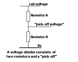
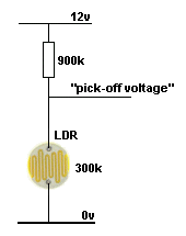
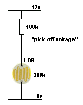
THE VOLTAGE DIVIDER Nearly ALL circuits (and
individual stages) use a VOLTAGE DIVIDER. A Voltage Divider is simply two
resistors connected in series.
However it may not be two resistors. It may be a resistor and a
transistor. A transistor is really a resistor - a variable resistor -
and they form a voltage divider with a resistor called the LOAD. Sometimes
more resistors are present
(such as resistors creating an H-bridge biasing network) and there may be more than one voltage divider in a stage.
However the same principle applies.
The principle is this:
CURRENT FLOWS THROUGH THE
COMBINATION (the current is the same for each
resistor because they are in series).
Multiply the current (in amps) by the resistance (in ohms) to get the
voltage across each resistor.
In most cases, the sum of the voltages across each resistor must
add up to the supply voltage.
Here are 2 examples of a VOLTAGE DIVIDER:
This is as far as we can go without using mathematics.
A "STAGE"
A "Stage" is a set of components with a capacitor at the input
and a capacitor on the output.
We have already seen the fact that the capacitor only has an effect on
the circuit during the time when it gets charged. It also has an effect
when it gets discharged. But when the voltage on either lead does not
rise or fall, NO CURRENT flows through the capacitor.
When a capacitor is placed between two stages, it gradually
charges. When it is charged, the voltage on one stage does not affect the voltage on
the next stage. That's why the capacitor is drawn as two lines with a
gap. A capacitor is like putting a magnet on one side of a door and a
metal sheet on the other. Moving the magnet up and down will move the
metal up and down but the two items never touch.
Only a rising and falling voltage is able to pass through the capacitor.
Fig 10. This is a
STAGE.
A transistor, with a capacitor
on the input and output.
Fig
10 has a capacitor on the input and output. This means the stage
is separated from anything before it and anything after it as far as the
DC voltages are concerned and the transistor will produce its own
operating point via the base resistor and LOAD resistor.
We have already explained that the value of the two resistors should be
chosen so the voltage on the collector should be half-rail voltage
and this is called the "idle" or "standing" or "quiescent"
conditions.
It is the condition when no signal is being processed.
When the voltage on the collector is mid-rail, the transistor can be
turned off a small amount and turned on a small amount and the voltage
on the collector will fall and rise. (note the FALL and RISE).
Fig
10a The LOAD resistor can be replaced with an inductor to
get an improved output signal.
Here is how the INDUCTOR works:
Because this circuit is so unusual in
operation, l am going to describe it this way:
Fig 10a. The LOAD
resistor is replaced with an inductor.
If you have followed the
operation of the
Joule Thief circuit (and more
HERE), you will know the transistor gets turned OFF
instantly when saturated and the inductor produces a very high
voltage with the positive emerging from the less connected to
the collector.
This means it produces a voltage that is ADDED to the supply
voltage.
Exactly the same thing happens in this circuit, but in the Joule
Thief the collapse is uncontrolled and the output voltage is
very high.
In this circuit the transistor is turned off very slowly and we
call this a CONTROLLED reduction in current.
The result is the inductor produces a voltage that increases
proportionate to the transistor turning off. As the transistor
turns OFF, its effective resistance increases and this allows
the magnetic flux to collapse and produce an output voltage.
This means the voltage on the collector will rise when the
inductor is added to the circuit.
When the transistor turns ON, it delivers an increasing current
into the inductor and this produces an expanding flux that cuts
the turns of the coil to produce a voltage at the wire connected
to the collector that is less than rail voltage and the
transistor will think it has a lower rail voltage. This means it
can pull down further when it is being turned ON.
The inductor improves (increases) the amplitude because energy
is not being lost in a resistor.
The two lines on the coil in the circuit above
represent a metal core.
The metal may be soft-iron for low frequencies or ferrite for
high frequencies.
Ferrite works up to about 250MHz and as the frequency increases,
the effectiveness of the core becomes less and less. Eventually
it becomes “1” and this is the value of air.
So air cored inductors are used for high frequencies and
although they do not produces voltages higher than the supply,
they do produce a reverse voltage (an opposing voltage) that is
used in the operation of the circuit. Whenever the voltage is
removed, the voltage produced by the coil, emerges as an
opposite voltage.
This voltage can be added to the supply voltage to get twice
rail voltage and this is an achievement. You need to see some of
our other discussions where this feature is explained.
The
FM Bug is a circuit that enjoys this feature.
Fig 11. The Input and
output
waveforms
Fig 11
shows a small waveform on the input and a
large waveform on the output. The increase in size is due to the
amplification of the transistor. A stage like this will have an
amplification of about 70.
This is called "Stage Gain" or "Amplification factor" and consists of
two things. The output voltage will be higher than the input voltage and
the output current will be higher than the input current.
We will discuss the increase in current and voltage in a moment.
We need to ask: Why is the gain of the stage only 70, when a
transistor with a gain of 200 is used?
The reason is due to the base-bias resistor. It is acting as a
feedback resistor and is acting AGAINST the incoming
signal.
For example, if the incoming signal is rising, the collector
voltage will drop and this will be passed through the base-bias
resistor to deliver less current to the base. This is opposing
the current being delivered via the signal and that's why it is
called NEGATIVE EFFECT or NEGATIVE FEEDBACK. Thus the transistor
cannot produce the output amplitude you are expecting.
Many text books state this type of stage has 180° phase-shift.
But because the output signal is decreasing at the same time the input
is increasing, the output is simply an inversion and NOT
phase-shift.
Fig 11a. Fixed Base
Bias
Fig 11b. Fixed Base
Bias
Fig 11a and 11b shows a Common Emitter
stage with fixed base-bias. This stage produces the maximum
voltage amplification but it is very difficult to "set-up"
because the value of the base resistor will either make the
collector voltage nearly zero or full rail voltage. It is very
difficult to get the collector to sit at mid rail.
If the base resistor is a high value, the collector will sit at
rail voltage. If the base resistor is a low value, the
collector will sit a 0v.
If a transistor with a different gain is fitted, the collector
voltage will change completely.
If it sits at mid-rail, the noise produced by the transistor
will make the collector voltage rise and fall and produce a lot
of noise.
It all revolves around the actual gain of the transistor and
this requires a TRANSISTOR TESTER to determine the gain.
However, this circuit can be used as an output stage and has some
advantages.
It is a "Class-C" stage and means it is just at the point of
being turned on via the base-bias resistor. It
consumes the least current when "sitting around" and
is the most
efficient stage.
Energy from a previous stage provides base current via the
coupling capacitor and the
base-bias resistor assists too.
The output waveform will be distorted at the top or bottom,
depending on the biasing and an inductor in the collector can reduce the distortion. See the article on FM Bugs (SPY BUGS) for
a Class-C output stage.
Unless you get the biasing correct, do not use this type of
stage as a general-purpose amplifier. If the transistor is
saturated (the base resistor is too low) the output will consist
of only the positive portions of the waveform and will be a lot
smaller than a self-biased stage.
Fig 12.
Fig 12
shows the signal (the voltage
waveform) as it passes through 2 stages. Note the loss in
amplitude as the signal passes through capacitor C2.
CONNECTING 2 STAGES
Before we discuss 2-stages of amplification, we need to cover a
few points.
Whenever you produce an amplifier, it will have GAIN. This means
the signal will be amplified. Normally a stage will have a gain
of 50 to 70 and two stages will produce a minimum of 2,500. If
you connect a “driver” stage, the voltage may not be increased
but the current through the output will be increased.
The
final amount of current is important because it has to be
delivered by the supply for part of the cycle and much less by
the other part of the cycle. This means the current requirement
goes up and down. The maximum current is called the PEAK.
No
supply is designed to give this PEAK current and so
electrolytics with a high value of capacitance (high microfarad
value) are placed across the supply. These are like miniature
batteries and they can supply this current very quickly.
Without them, the voltage of the supply would fall and return
quite noticeably and this is called “ripple.” When the
electrolytics are connected, the ripple reduces.
But you cannot reduce or remove all the ripple and a small
amount may be present on the supply rail.
This ripple looks exactly like the signal entering the amplifier
and it will be fed back to the first stage.
The signal might only be a few millivolts, but the input signal
will be as small as 10mV and so the ripple is a factor in the
following problem.
The supply voltage on the first stage will rise and fall and the
stage will include this ripple into its output.
This ripple will be a low frequency that the supply
electrolytics cannot deal with. It is a frequency that charges
and discharges the electrolytics very slowly and to reduce a low
frequency signal you need very high value capacitors.
So, this frequency is completely different to the frequency you
are supplying to the input and it get amplified, along with your
signal and appears on the output with an increased amplitude.
It could not be prevented before and it cannot be reduced now.
So it appears in the speaker as a noise similar to a motor
boat. That's why we call it MOTORBOATING.
We
have shown how to reduce and/or remove the effect in another
article.
The second point to note is this: You cannot keep increasing the
amplitude to a point higher than FULL RAIL VOLTAGE.
As
soon as you get SATURATION, you just need an output stage that
increases the current to produce the loudest output.
In general, this will require two stages of amplification and an
OUTPUT STAGE.
The following discussion covers different arrangements for the
2-stages of amplification.
There are 3 ways to connect two stages: 1.direct coupling - also called DC coupling
(not the coupling shown in fig 12.
Fig 12 is AC coupling). DC stands for Direct Current. I know
this sounds unusual, but it is the way to explain the circuit will
pass (amplify) DC voltages. This type of coupling will pass both AC
signals and DC voltages. When the DC voltage moves up and down
(even at a slow rate) we call it an AC voltage or AC signal or a
rising and falling voltage and when it rises and falls faster,
we call it a "signal" or waveform. 2.via a capacitor - this is also called RC coupling
(Resistor-Capacitor coupling) - only passes AC signals -
fluctuating signals - rising and falling signals. 3.via a transformer - called Transformer Coupling or
Impedance Coupling or Impedance Matching - only passes AC
signals.
Fig 12 shows two stages with a capacitor coupling the output of
the first to the input of the second. This is called
Capacitor Coupling or Resistor-Capacitor Coupling (RC
Coupling).
The increase in the size of the
waveform at three points in the circuit is also shown.
The waveform is inverted as it passes through each transistor and this
simply means a rising voltage will appear as a falling
voltage and after two inversions, the output is in-phase with the input.
We have already explained the fact that a capacitor only works once and
has to be discharged before it works again. When the first
transistor turns off a little, the voltage on the collector rises and
the resistor pulls the left lead of C2 UP. The right-hand lead can only
rise to 0.7v as the base-emitter voltage does not rise above 0.7v.
This means C2 charges and during its charging, it delivers current to
the second transistor.
When the first transistor turns ON, the collector voltage drops and C2
passes this voltage-drop to the base of the second transistor. But the
transistor does not provide a path to discharge the capacitor fully so
that when the capacitor gets charged again, it is already
partially charged and it cannot activate the base of the second
transistor to the same extent as the first cycle.
This means a lot of the energy available at the collector of
the first transistor is not delivered to the second stage. That's why
capacitors produce losses between stages. They are simply an
inefficient way to transfer energy. To make them efficient, they
must be discharged fully during the "discharge-part" of the
cycle.
However enough is delivered to produce a gain in the second stage to get
an overall gain of about
70 x 70 for the two stages.
The value of C2 will be from 10n to 10u, and the larger capacitance will
allow low frequencies to be passed from one stage to the other.
Fig 13.
Fig 13 provides a guide to the values of current
that will be flowing at 3 important sections of the circuit.
The input current to operate the first transistor will be about
3uA. This is worked out on the basis of the current required to
saturate the transistor with a 22k load. The collector-emitter current
equals
5/22,000 = 200uA. If the gain of the transistor is 70, the input current
is 3uA.
The only time when energy passes from the first stage to the second is
when transistor turns OFF. The collector voltage rises and the 22k pull
the 100n HIGH.
The maximum current that can be delivered by the 22k is 5v/22,000=
200uA. This is the absolute maximum for a very small portion of the
cycle. However it is important to realise it is not the transistor that
passes the current to the next stage but the load resistor.
The gain of the second stage is not the deciding factor for the output
current but the value of the 2k2 load resistor. This resistor will
deliver a maximum of 2,000uA (2mA) and that is how a 3uA requirement at
the input of the circuit will deliver 2mA at the output.
You can see it is not the gain of the transistors that produce
the output current but the value of the load resistors. The transistors
play a part but the limiting factor is the load resistors (and the
transfer of energy via the capacitor). This is not
always the case but applies in the above circuit.
We will now explain an emitter-follower stage and show how it works.
An EMITTER-FOLLOWER is an NPN transistor with the collector
connected to the positive rail. (You can also get PNP EMITTER-FOLLOWER stages - see below).
Both can be called a COMMON COLLECTOR stage.
Fig 14. An
Emitter-Follower or
Common Collector.
The names are the SAME
Fig 14 shows an
Emitter-Follower.
The load is in the emitter and as the base is taken higher, the emitter
follows. But the input and output voltage signals are the SAME amplitude!
You would ask: "What is the advantage of this?"
Answer:
You only need a small amount of "lifting power" to raise the base and
the emitter rises with 100 times more strength. The voltage waveform
stays the same but the CURRENT waveform increases 100 times.
The voltage on the emitter is always 0.7v lower than the base and the
base can be as low as 0.8v and as high as 0.5v less than the supply
voltage. This gives the possibilities of producing an enormous "swing."
In the common-emitter stage the transistor is only active
when the base rises from 0.55v to about 0.7v but
in the Emitter-Follower stage it rises from 0.8v to
nearly rail voltage.
This means the stage does not produce a higher output voltage but it
does produce a higher output CURRENT.
We mentioned before the current amplification of a stage was not
dependent on the transistor characteristics but the value of the load
resistor. In an Emitter-Follower stage we can quite
easily get a current gain of 100 or more.
Why do we want "Current Gain?"
We need current to drive a low resistance load such as a speaker.
Fig 15. A transistor
driving a speaker
Fig 15
shows an 8 ohm speaker as the load in the emitter. If the gain of the
transistor is 100, the 8R speaker becomes 8x100 = 800 ohms on the base
lead. In other words we see the circuit as "800 ohms."
See this link for
the answer to a constructor. He wanted to increase the output
from his mobile handset.
1.
For an emitter-follower circuit, we know the base can rise and fall by an amount equal to about rail
voltage. 2. For a common-emitter stage the collector rises
and falls by an amount equal to rail voltage.
So, why not connect the two stages together without a capacitor?
We know a capacitor has considerable losses in transferring energy
from one stage to another and removing it will improve the transfer of
energy.
Fig 16. Two directly
coupled stages
Fig 16. We now
have two stages directly connected together.
The first transistor does not deliver energy to the second stage but the
LOAD RESISTOR does.
The
value of the load resistor pulls the base of the second transistor UP and
this delivers current to the second transistor and the transistor
amplifies this 100 times to drive the speaker.
Fig 17. The load resistor
and the effective load of the speaker
Fig 17.
Using mathematics we can work out the effective load of the 8 ohm
speaker as 8 x 100 = 800 ohms. To put at least half rail voltage
into the speaker, (so the speaker can get the maximum
higher voltage and the maximum lower voltage without distorting) the LOAD
resistor has to be the same value as the "emitter follower."
This is a simple voltage-divider calculation where two equal
value resistors produce a voltage of 50% at their mid-point.
This means the LOAD resistor for the first stage has to be 800 ohms.
Fig 18. The load resistor
is 800 ohms
Fig 18 shows the circuit with 800R load resistor
in the collector of the first transistor.
The final requirement is to select a base-bias resistor for the first
stage to produce approx mid-rail voltage on the collector.
This is generally done by experimentation.
8R SPEAKER Vs 50R
SPEAKER
Most of the speakers used in
transistor radios have an impedance (resistance ) of 8R for the
VOICE COIL. This has been chosen because it is very easy and
cheap to produce. The wire in the coil is also quite thick and
robust.
But it is interesting to note that speakers with a high
resistance voice coil will produce an equal volume and require
less driving current. This applies to 33R speakers as well as
50R speakers.
The reason is this:
Moving the cone requires a certain amount of flux and this can
be produced by a small number of turns and a high current or a
large number of turns and a low current.
The flux is a product of turns x current and this is
called AMP-TURNS. In other words, AMPS x TURNS.
If you find a 33R or 50R speaker in a kit, you will know it will
perform just as loud as an 8R speaker.
We mentioned the capacitor separating two stages cannot be
discharged fully and thus it does not provide very good transfer of
energy from one stage to the other.
An improved concept is to directly couple two stages - and remove the
coupling capacitor.
This is called DIRECT COUPLING or DC coupling and the circuit will
process DC voltages (the press of your finger as shown above) and AC
voltages (as shown by the sine-wave signal shown above). When a
capacitor connects two stages they will only amplify AC signals.
There are many ways to directly connect two transistors and we will
cover the simplest arrangement. It is an extension of
Fig 18 above, because this arrangement has very
good characteristics as the two stages transfer 100% of the energy
due to the absence of a capacitor.
Fig 19.
Fig 19 shows the previous directly-coupled circuit with a load resistor
replacing the speaker.
We have already learnt the common-emitter stage provides a voltage gain
of about 70 but the emitter-follower stage has a voltage gain of only 1.
We can improve this by putting two resistors on the second transistor
and changing the stage into a common emitter arrangement.
Fig 20.
Fig 20.
This time we get the advantage of the base being able to move up and
down so it matches the collector of the first transistor. It also
provides a higher voltage gain by adding a collector resistor
and taking the output from the collector. The voltage gain of
the second transistor will not be as high as the first stage but we have added the
advantage of direct coupling (called DC coupling).
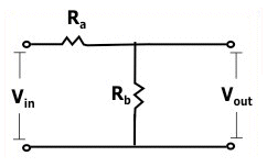
The voltage gain of the second stage is the ratio of resistor A divided
by resistor B. If resistor A is 10k and resistor B is
1k, the voltage gain is 10,000/1,000 = 10.
Fig 21.
Fig 21
shows biasing of the first transistor has been taken from the emitter of
the second transistor. This does not save any components but introduces
a new term: FEEDBACK
(actually NEGATIVE FEEDBACK).
Negative feedback provides stability to a circuit.
Transistors have a very wide range of values (called parameters) such as
gain and when two
transistors are placed in a circuit, the gain of each transistor can produce an
enormous final result when the two values are multiplied together.
To control this we can directly couple two transistors and take the
output of the second to the input of the first.
Fig 22.
Fig 22.
When the
voltage on the base of the first transistor rises, the voltage on the
collector drops and this is transferred to the
second transistor. The voltage on the emitter of the second transistor
drops and this is fed back to the base of the first transistor to oppose
the rise. Obviously this arrangement will not work as the voltage being fed back
is HIGHER than the signal we are inputting, but if we add a 220k
resistor
we can force against the feedback signal and produce an output.
Fig 23.
Fig 23. We have added a capacitor (electrolytic) to the emitter of the second
transistor. Let's explain how this electrolytic works.
An electrolytic is like a miniature rechargeable battery.
It charges very slowly because it is a large value.
Initially it has 0v.
The circuit starts to turn ON by current flowing through the load
resistor and this turns on the second transistor. (The first transistor is not
turned on AT ALL at the moment).
The base rises and pulls the emitter up too. And when the emitter is about 0.7v, this voltage is
passed to the first transistor via the 220k and the first
transistor starts to turn on. This causes current to flow through the
collector-emitter leads and pulls the voltage on the base of the second
transistor down to about 1.4v
This is how the two transistors settle, with the voltages shown in
Fig 23.
The electrolytic has 0.7v on it and when a signal is delivered to the
base of the first transistor, it is amplified and passed to the emitter
of the second transistor. Normally the emitter would rise and fall as
explained in the above circuits and the result would be heard in the
speaker. But the electrolytic takes a long time to charge (and
discharge) and it resists the rise and fall of the signal.
This means the signal cannot rise and fall at the emitter.
In other words we have placed the second transistor in a stage very
similar to the first stage we described a COMMON EMITTER.
Since the emitter voltage does not rise and fall, it does not pass a
signal through the 220k to the base of the first transistor. This means
our input signal is not fighting against the feedback signal and it has
a larger effect on controlling the first transistor. This gives the
first transistor a bigger gain.
A common emitter stage has a voltage gain of about 70-100 and we now
have one of the best designs. Two common-emitter stages, directly-coupled
(DC) and with very HIGH GAIN. The feedback only controls the DC
voltages on the two transistors and does not have an effect on the AC
(signals).
Fig 24.
Fig 24a is the best circuit you can get
for amplifying a signal. The two transistors are biased via
the 470k feedback resistor so they are turned ON and ready to
amplify the signal. There is no capacitor between the two
transistors so the overall gain is very high.
Fig 24 shows typical values for biasing the two transistors.
This circuit has been tested with a speaker as the input device.
It produces 2mV with a whistle at 30cm and the output produced a
sinewave of 3,000mV (a gain of 1,500)
The component values are show in Fig 24a:
Fig 24a - the
best
circuit you can get.
This circuit is also
called a WIDEBAND AMPLIFIER because it will amplify all frequencies.
From what you have learnt, you can see the
mistakes and/or the voltages in the following circuit:
Fig 25.
Fig 25.
The two joined transistors create a Darlington transistor
and this is just a normal transistor with a large gain.
The 330R discharges the 100u and it will only discharge it a very small
amount. This means the electro can only be charged a very small amount
during the next cycle
and the output will be very weak.
It is the 330R that determines how much (little) energy gets
delivered to the speaker. The 330R has to be 15R to nearly fully discharge
the 100u.
Fig 26.
Fig 26.
You can work out the voltage on the various points in this
circuit by referring to the examples we have already covered.
Fig 27.
Fig 27. This is
a practical example of the circuit we have discussed. It is a
MICROPHONE AMPLIFIER (also called a pre-amplifier stage).
Fig 27a.
Fig 27a.
Here is the same circuit used as a POWER AMPLIFIER.
Both transistors are common-emitter configurations and the
circuit produces high gain due to the DC (direct) coupling.
Fig 27b.
Fig 27b.
You can create a circuit with a FIXED GAIN by selecting values
for the gain of each stage. This is calculated by dividing the
collector resistor by the the emitter resistor.
For the first stage, the gain is 22,000/220 = 100. The gain of
the second stage is 10,000/470 = 20. The gain for the two stages
is 100 x 20 = 2,000. See
Stage Gain
for more details.
CONNECTING 3 STAGES
Before we continue, I need to include a circuit that directly
couples 3 transistors.
Normally, this is very hard to do because the gain of each
transistor is about 50, making the total 50 x 50 x 50 =
125,000 so that 1mV signal will become ENORMOUS at the output.
This amplitude will feedback to the front-end to create
motor-boating and squealing.
Secondly, it is very difficult to bias 3 directly coupled
transistors. This circuit has overcome some of these problems by
creating a biasing feedback via the 6k8 resistor to DC adjust
the biasing of the first transistor and this transistor has an
effect on biasing the other two transistors.
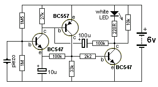
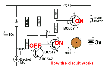
This 3-tranisistor circuit needs to do two
things. It needs to amplify the voltage of the signal and also
the current. The output of the electret mic is about 10mV and
the signal on the collector of the first transistor is about
300mV. The current capability of the signal will also be
increased, but its value is not important.
The second transistor increases the voltage and the current and
is classified as a COMMON EMITTER stage. What it is really
doing is "squeezing" or closing-up the emitter-collector leads
and in doing this, it is pulling the third transistor up and
down. This is because the third transistor is an EMITTER
FOLLOWER and it is rising and falling and pulling up the top
wire of the earpiece. In doing this it is injecting a signal
into the earpiece and this is what we hear.
It takes a lot of current though the earpiece to produce a
voltage across the earpiece and this is how the top wire rises.
The third transistor increases the base current about 50 to 100
times but it does not increase the voltage. The voltage is
already a maximum via the first and second transistors.
So, we have the circuit producing about 2.5v output from 10mV
signal and 35mA output from a signal of less than about 0.2mA .
The whole circuit is self-biased via the 6k8. The first
transistor turns on fairly fully via the 1M. This turns ON the
second transistor very hard and the third transistor turns on
FULL too.
This puts a high current through the earpiece and a voltage is
developed across the earpiece.
This voltage flows through the 6k8 and charges the 100u
electrolytic. Very soon the voltage on the emitter rises
and this makes the base rise. The voltage across the 1M resistor
reduces and thus the current into the base reduces and the first
transistor turns off a small amount and this is passed to the
other two transistors. In this way the circuit settles at a
point where all the transistors are about half turned-on.
This circuit does not produce instability because the voltage
gain of the 3 transistors is 30 x 10 x 1 = 300. However the
inclusion of the 100u across the battery improves the
sensitivity and clarity of the sound by preventing the signal
disappearing into the 3v coin cell.
The POWER of a SIGNAL
Before we go too much further, we need
to talk about the POWER OF A SIGNAL.
What is a SIGNAL?
A Signal is a voltage produced by a microphone, an
inductor, or the output from a previous stage.
It may be the signal for the "input" of the amplifier in Fig 27a
above, or it may be the resistance of your finger in the
circuits above, or it may be the signal from a single stage shown above (as a sinewave).
A signal may be an audio waveform with a very small
amplitude or a DC voltage from a switch or a digital
signal from a chip or the output from one of the stages
shown above.
In all these instances we have described the amplitude
of a signal. The amplitude is the VOLTAGE of the
signal.
But a signal consists of a VOLTAGE and comes with a
value of CURRENT. This current may be very small (such
as from an electret microphone) or it may be very high
(such as from a switch).
In most cases we do not talk about the value of current
associated with the signal. Mainly because it is a very
complex problem, matching-up the
"current-capability" of the signal with the "current
requirement" of the following stage.
At this point we will simply say that ALL signals come
with a VALUE OF CURRENT. And this is called "The Power
of a SIGNAL." In other words: The STRENGTH of a Signal"
or the "Driving capability of a signal.
We can also say a signal is "very weak" or "delicate" or
"strong" or "has good driving capability."
Some signals will drive a LED or speaker while others
need to be amplified before they can be used.
In most cases the "driving power of a signal" is unknown.
It is not provided as a specification. And yet its
value is MOST IMPORTANT. In most cases you cannot work
out the current-capability of a signal by looking at the
device generating the signal. For instance, if the
signal comes from a magnetic pick-up coil, or the output
of a pre-amplifier where the circuit is not provided.
That's why the matching of a signal to an input circuit
is so complex and is a topic for an advanced section of a
discussion.
In the meantime we will assume the signal and the input
of the stage it is driving, has the appropriate input
impedance so the signal is not attenuated (reduced)
too much.
If a signal has a high current it can be connected to
a high or low impedance input and the amplitude will not
be affected.
If a signal with very little current
is connected to the input of an amplifier and the input
has a low impedance, the amplitude of the signal will be
reduced. That's why the input needs to be as high
as possible.
Maximum POWER is delivered from one stage to the next
when the impedance of the source matches the impedance
of the load.
Maximum VOLTAGE is delivered from one
stage to the next when the impedance of the source is
LOW and the impedance of the load is HIGH.
USING PNP TRANSISTORS
A PNP transistor can be used
in the 2-Transistor DC amplifier studied above. It does not produce a
higher gain or change the output features of the circuit in any way but you may
see an NPN and PNP used in this configuration and need to know how they work.
Firstly we will discus how a PNP transistor works. All those things you
learnt in the first set of diagrams can be repeated with a PNP
transistor. The circuits are just a mirror-image of each other and
the transistor is simply "turned-over" and connected to the supply rail.
Study the following circuits to understand how a PNP transistor is
TURNED ON.
Fig 28. PNP Transistor
Symbol
Fig 28.
The symbol for a PNP transistor has the arrow pointing towards
the BASE.
You will notice the transistor is drawn with the emitter-lead at
the top of the page as this is how it will be connected in a
circuit. The emitter is generally connected to the positive rail
and the arrow shows the direction of the current.
You MUST refer to a data sheet for the actual pin connections.
Fig 29. PNP
"Water Valve"
Fig 29
shows the equivalent of a PNP transistor as a water
valve. As more current (water) is released from the base, more water flows from
the emitter to the collector. When no water exits the base, no water
flows through the emitter-collector.
Fig 30. PNP
connected to the power rails
Fig 30
shows a PNP transistor with the emitter lead connected to the power rail.
The collector connects to a resistor called a LOAD RESISTOR and the
other end connects to the 0v rail or "earth" or "ground."
The input is the base and the output is the collector.
Fig 31. PNP Transistor biased with a
"base bias" resistor and a LOAD resistor
Fig 31
shows a PNP transistor in SELF BIAS mode. This is called a
COMMON EMITTER stage and the resistance of the BASE BIAS
RESISTOR is selected so the voltage on the collector is
half-rail voltage. In this case it is 2.5v.
Here's how you do it. Use 22k as the load
resistance.
Select the base bias resistor until the measured voltage on the
collector is 2.5v. The base bias resistor will be about 2M2.
This is how the transistor gets turned on by the base bias resistor:
The base bias resistor allows a small current to pass from the emitter
to the base and this
makes the transistor turn on and create a current-flow though the
emitter-collector leads.
This causes the same current to flow through the load resistor and a
voltage-drop is created across this resistor. This raises the voltage on
the collector.
This causes a lower current to flow from the emitter to the base, via the
base-bias resistor, and the transistor stops turning on a slight amount.
The transistor very quickly settles down to allowing a certain current
to flow through the emitter-collector and produces a voltage at the
collector that is just sufficient to allow the right amount of current
to flow from the base. That's why it is called SELF BIAS.
Fig 32. Turning
ON an PNP transistor
Fig 32 shows the transistor being turned on via a finger.
Press hard on the two wires and the LED will illuminate brighter. As you
press harder, the resistance of your finger decreases. This allows more
current to flow from the emitter to the base and the transistor turns on harder.
Fig 33. Two transistors turning ON
Fig 33
shows a second transistor to "amplify the effect of your finger"
and the LED illuminates about 100 times brighter.
Fig 34. Adding a capacitor
Fig 34
shows the effect of putting a capacitor on the base lead. The
capacitor must be uncharged and when you apply pressure, the LED
will flash brightly then go off. This is because the capacitor
gets charged when you touch the wires. As soon as it is charged,
NO MORE CURRENT flows though it. The first transistor stops
receiving current and the circuit does not keep the LED
illuminated. To get the circuit to work again, the capacitor
must be discharged. A large-value capacitor will keep the LED illuminated for
a longer period of time as it will take longer to charge
Fig 35.
Adding a capacitor to the
output
Fig 35 shows the effect of putting a capacitor on the
output. It must be uncharged for this effect to work. We know from
Fig 33 that the circuit will stay on constantly when the wires are
touched but when a capacitor is placed in the OUTPUT, it gets charged
when the circuit turns ON and only allows the LED to flash.
THE
NPN/PNP AMPLIFIER A
2-Transistor DC amplifier can be
constructed using an NPN and PNP set of transistors.
Fig 36.
Fig 36 shows how an NPN-PNP set of transistor is turned on.
You can think of the "turning ON" this way: The base of the NPN
get "Pulled UP" and the base of the PNP gets "Pulled DOWN."
It does not matter how you refer to the operation of the circuit, you
must be able to "SEE" how the circuit works so you can
see a
more-complex circuit working too!
Fig 37.
Fig 37 shows biasing on the base of the first transistor and the "in"
and "out" leads have been identified.
This circuit has a very high gain and if "general purpose" transistors
are used with a very high spread of gain for each transistor, the result
will be a very wide range of voltages on the output terminal. If
each transistor has a gain of 100, a change of 1mV on the input will
result is a voltage change of 0.001 x 100 x 100 = 10v. We don't
have a 10v supply so, this type of circuit is very UNSTABLE!
We need to design a circuit that has FEEDBACK so the output voltage will
remain within the voltage of the supply. This feedback is called
NEGATIVE FEEDBACK as it opposes an input signal to provide correction or
stability. Later we will talk about POSITIVE FEEDBACK and show what an
amazing difference it creates - the circuit behaves totally differently.
Fig 38. This circuit does
not work
Fig 38
will not work because the base of the NPN transistor is not
turned on when the circuit is switched on.
This is one of the things you have to look for when designing a
circuit.
Fig 39. The voltages
Fig 39 has
a voltage-divider network on the base of the NPN transistor. It
turns the first transistor ON and this turns the PNP transistor
ON until the voltage at the join of the 3k3 and 1k puts a
voltage on the emitter of the first transistor to start turning
it OFF.
This is a point we have to explain.
There are two ways to turn ON an NPN transistor.
1. Hold the emitter fixed and RAISE the base voltage.
2. Hold the base fixed and LOWER the emitter voltage.
In Fig 39
the base is weakly fixed by the voltage divider made up of the
1M and 220k and even though the base can move up and down a little bit, we will
assume the voltage is constant. If we raise the emitter voltage, the
transistor will be turned off. This is what the FEEDBACK voltage via the
3k3 does. It raises the emitter voltage and turns the NPN transistor OFF
slightly so an equilibrium point is reached where the two
transistors are turned on a small amount and
if one gets turned on a
little more, the other sends signal to turn it OFF. This is not a
practical circuit as an increase of 1mV on the input will produce a
large change on the output and this will be reflected back to the
emitter of the first transistor to cancel the input voltage.
Fig 40. A practical
example
Fig 40.
By changing the value of the feedback resistors we get Fig 40. The values are now 10k and 100R.
This gives a ratio of 10,000:100 or 100:1 and it means the output can
rise 100mV before the emitter gets 1mv to cancel the input voltage. This
means the amplifier will have a gain less than 100 but provides a very
stable set of voltages.
Fig 40a. Another practical
example
Fig 40a.
Here is an amplifier with the same DC
biasing as Fig 40 but with a lower overall gain (2,200:100
or 22:1) and high-frequency feedback
(attenuation) via the 2n2 capacitor.
GAIN
There are thousands of different types of transistor(s)
on the market because in the early days of producing a
transistor, the manufacturer could not a make a batch with all the same
characteristics.
So they sorted them after manufacture.
The two main things that varied was the voltage that could be
placed across the collector-emitter leads of the transistor
before it started to leak (pass current) or before it stared
to zener (pass a lot of current) And the other feature was
the gain of the transistor. It is the
amplification-capability of the transistor and is basically
the amount of current entering the base of the transistor
(the current you deliver to the base) compared to the
current flowing through the collector-emitter leads (this is
called the LOAD current as this current will also pass
through the load).
If you are using a supply up to about 20v, almost any
transistor can be used and the only decision is the GAIN of
the transistor.
Almost every small signal transistor has a gain over 100 and
and although you can get a transistor with a gain of 200,
300 or 400, these transistors will produce almost the same
result when they are placed in a circuit.
You may get slightly better performance with a high gain
transistor, but don't be surprised if the outcome is hardly
detectable.
That's why you should use a transistor from the mid-range
and not design a circuit with the expectations of always
using a high-gain transistor.
Power transistors have a gain (CURRENT GAIN) as low as 10 to
70 and one transistor from a batch may be 25 and another 55.
That's why you need to try a few transistors and see if a
poor-quality device still works in the circuit you have
designed.
The gain figure in the data-sheet is quite often determined
when the collector current is 1mA or 10mA and when it passes
say 100mA, the gain will be a lot less.
You cannot build a circuit and multiply the gains of the
transistors from the data-sheet to get a result.
The gain of the transistor in a data-sheet is determined
under IDEAL conditions with DC voltages. When you put this
transistor in an audio circuit (for example) the gain is
completely different. This time it is not the high current
flowing but due to the surrounding
components determining how the transistor
is biased.
Some of these components stabilize the operating conditions
for the transistor and to do this they create feedback
within the stage and this feedback reduces the gain
enormously.
The end result is a 100, 200, 300, 400 gain transistor will
produce the same 70 times gain for the stage. Of course this
is all generalisation, but it lets you know why the end
result is almost the same with any transistor, (although you
have tried transistors with widely varying characteristics).
The CAPACITOR The capacitor is a
very complex item to discuss because it
performs with so many different effects, depending on its value and
where it is placed in a circuit.
However one of the most important concepts is to see that a
signal on the left side will pass through the capacitor and
appear on the other side with about the same amplitude, if
the signal is fast-acting. In other words: high-frequency.
This is shown in the first animation where the movement of
the first person is transferred directly to the second
person.
If the signal has a low-frequency, is will get charged and
discharged during the cycle and the amplitude on the output will be small. This is shown in the second animation where
the capacitor is charging and discharging and the second
person is seeing a small effect.
The circuit shows a Schmitt
Trigger arrangement. This is covered
HERE.
The Schmitt Trigger is FAST ACTING and this means
the signal on the left-plate of the capacitor will be delivered
to the output of the circuit.
Delivering 100% of the amplitude will depend on:
1. The value of the
capacitor,
2. The rise-time of the signal and
3. The load on the
right-plate of the capacitor.
At the moment we just need to VISUALISE the way the capacitor
will
work.
The capacitor will pass a "spike" or "signal"
from one stage to another:
The capacitor sending (transferring) a PULSE to the
DIGITAL GATE.
This is a VERY IMPORTANT concept.
The capacitor in the diagram is
transferring the "drop in voltage" on the left-plate to the
right-plate.
The voltage on the input to the DIGITAL NAND GATE is initially rail
voltage and it must drop to less than 30% of rail voltage for
the gate to see a LOW.
The value of the capacitor is chosen so this will occur.
When the voltage on the left-plate drops, the capacitor will
begin to charge via the 1M resistor and the circuit-designer
must make sure the charging of the capacitor will be very small during the time
when the voltage drops so the right-plate will send a 30% rail
voltage to the gate. If the value of the capacitor
is too small, it will get charged very quickly and the right-plate will only
drop a small percentage of rail-voltage.
MEASURING THE VOLTAGE(S)
The voltage on each
line (connection) of a circuit can be measured
with a multimeter. To help you take (make) a
reading, we have written an eBook titled: Testing Electronic Components.
There is a certain amount of skill required to
take a reading and this eBook will help you
enormously.
OSCILLATORS
If we remove some of
the components from Fig 39 and put a LED on the emitter of
the PNP transistor we have a circuit that will illuminate the LED.
We have already talked about FEEDBACK in terns of NEGATIVE FEEDBACK to
stabilize a circuit. We will now cover a new term called
POSITIVE
FEEDBACK
- it changes the performance of circuit completely.
It makes the circuit OSCILLATE. Negative feedback "kills" a
circuits performance - positive feedback makes it oscillate. It
increases the signal so much that the circuit becomes unstable. This is
called oscillation.
Fig 41.
Fig 41 shows
a circuit using an NPN and PNP connected via a 1k resistor and turned ON
via a 330k base resistor.
The LED will illuminate.
There is nothing magic about this circuit. It is simply a HIGH-GAIN,
DC-AMPLIFIER using two transistors.
The values of
current are only approximate and show how each section allows an
increasing amount of current to flow.
A current of 100mA is too high for a LED and it will be damaged.
This circuit demonstrates the possible current-flow. If this
current flows for a very short period of time, the LED will not
be damaged. Fig 42 shows how the circuit is converted to an
oscillator or "flasher."
Fig 42.
Fig 42.
When we connect a capacitor as shown,
an amazing thing happens. The high-gain amplifier turns into an
OSCILLATOR.
When the voltage on point "X" is rising, the voltage on point "Y" is
rising TOO. But point "Y" rises much higher than point "X."
This means that if we DIRECTLY join points X and Y, the voltage-rise from point Y
will push point X higher and turn the circuit ON more. This will
continue until the circuit is fully turned ON and the two transistors are
SATURATED.
This effect is called POSITIVE FEEDBACK and the circuit will get turned
ON until it cannot turn on any more.
But we haven't joined points "X" and "Y" DIRECTLY
(we have used a capacitor) so we have to start again and
explain how the circuit works.
When the power is applied, the 10u gradually charges and allows a voltage
to develop on the base of the NPN transistor. When the voltage reaches 0.6v, the
transistor turns ON and this turns on the PNP transistor.
The voltage on the collector of the PNP transistor increases and this
raises the right side of the 10u electrolytic and it firstly pushes its
charge into the base of the NPN transistor. Then the 330k takes
over then it continues to charge in the opposite direction via the base-emitter junction of the
NPN transistor. This causes the two transistors to turn ON more. This
keeps happening until both transistors cannot turn ON any more and the
10u keeps charging. But as it continues to charge, the charging current
eventually drops slightly and this turns off the first transistor
slightly. This gets passed to the PNP transistor and it also turns off
slightly. This instantly lowers both leads of the 10u and both
transistors turn OFF.
The 10u is partially charged and it gets discharged over a long period
of time by the 330k resistor and when it starts to charge in the
opposite direction, the base of the first transistor sees 0.6v and the
cycle starts again.
The end result is a very brief flash and a very long pause (while the
capacitor starts to charge again).
As you can see, there is very little difference between the high-gain DC
amplifier we discussed above and the oscillator circuit just described.
That's why you have to be very careful when looking at a circuit, to
make sure you are identifying it correctly.
REGENERATION
From the animation
above, you can see the two transistors disappear from the
circuit during part of the cycle. This means the transformer
will have no connection to the bottom lead and the magnetic flux
in the core will be able to collapse very quickly and produce a
very high voltage. This voltage is reduced when the secondary
has a load.
If
an inductor is used in the LOAD, it will produce a back voltage
as high as 100v or more and this will be zener-reduced by the
transistor you are using to drive the coil. was taken to the grid (input) and this was
passed through the valve again.
This feedback signal had to be controlled to prevent
self-oscillation (that completely drowned out the radio signal).
The circuit uses regeneration to completely turn ON the LED. If
is were a radio, the output would be completely distorted,. But
that's the difference between audio and digital.
The 10u provides a much-higher base current into the NPN
transistor than supplied by the 330k and this guarantees the LED
will flash very brightly.
But it is important to realise the 10u not only provides the
flash-rate of the circuit but the very bright flash. Now: the act of regeneration: The 330k turns ON the NPN
transistor very slightly. This turns ON the PNP transistor 100
times harder. But the 22R in the collector is a very low
resistance and the current though it (at the moment) produces a
very small voltage.
However this voltage is passed to the base of the NPN transistor
via the 10u to turn it on slightly more.
At this point in the cycle, you can consider the 10u to be a
very small rechargeable battery and if the right lead is raised
a few millivolts, the left lead will rise about the same amount.
The 10u now provides current into the base of the NPN transistor
to turn it on.
As the two transistors turn ON more and more, the right
lead of the 10u rises and when it is higher than 0.65v, the 10u
starts to charge via current flowing through the base-emitter
junction of the NPN transistors. It is this current that turns
the NPN transistor ON more and the resistance of the
collector-emitter circuit becomes very small. This allows a high
current to flow in the emitter-base leads of the PNP transistor
as the only resistor limiting the current is 1k. Between nearly
3mA and 6mA will flow, depending on the supply voltage and if
the transistor has a gain of 50, the collector current has the
possibility to the 50 x 6 = 300mA. This amount of current
will not be flowing because the LED has a characteristic voltage
3.4v and this value must be subtracted from the supply voltage
to get some idea of the maximum current that will be flowing.
However, the creation of a high current pulse is due to the 10u.
FEEDBACK OSCILLATOR . . . also a FLYBACK OSCILLATOR
In this next circuit we change the position of the components
from the circuit above and it will operate exactly the same. It
has a very short ON time and a long OFF time. This can be shown
if we add a LED to the LOAD.
Then we will use a transformer as the LOAD and the output
will flash a red LED and green LED.
The circuit starts in the OFF state and the
capacitor charges via the 10k and 330k.
This takes a long time and produces the long OFF time.
When the base of the PNP transistor sees a voltage about 0.6v
below rail voltage, it turns ON and this action turns on the NPN
transistor. This pulls the positive lead of the 1u electrolytic
down and the small voltage it contains is delivered to the PNP
transistor to turn it ON harder. The right lead of the capacitor
is now pulled down to almost 0v via the NPN transistor and now
the capacitor starts to charge via the 10k resistor and the
base-emitter junction of the PNP transistor. Eventually the
capacitor is fully charged and the current through the PNP
transistor base reduces to a point where the transistor is not
turned ON as much and this starts to turn OFF the NPN
transistor. The voltage on the collector of NPN rises and raises
the 1u and this completely turns OFF the PNP transistor. The
voltage on the base of the PNP is actually higher than rail
voltage and the 1u is gradually discharged via the 10k and 330k
to repeat the cycle. Because this circuit has such a fast change
from one state to the other it is classified as a flyback
arrangement or flyback circuit.
But we mainly want to explain how the capacitor works . .
electrolytic
HOW THE CAPACITOR WORKS
At
the start, the 1u is charged via the 1k, 10k and 330k. As soon
as the PNP transistor sees a voltage on the base that is 0.6v
lower than the supply of 6v, it starts to turn ON. This action
will turn on the NPN transistor.
The 1u electrolytic will be pulled down by
the NPN transistor, and cause it to be charged at a higher
current via the collector-base junction of the PNP transistor
and 10k resistor. This higher current makes the
PNP turn ON more. Eventually the 1u will be fully charged and
the PNP will turn off a small amount and this action will turn
off the NPN transistor.
The fully charged capacitor will rise high in the circuit and
produce a voltage on the base of the PNP transistor that is
higher than rail voltage.
At this point the two transistors are "out of circuit" and the
components will discharge the capacitor to produce the "OFF
time."
When the cap fully discharges it begins to charge in the
opposite direction to start the cycle again.
Feedback Oscillator Animation
You need to view the animation a number of
time to get the full concept of what is happening. The voltage
on the base of the PNP transistor will be higher than the rail
voltage for part of the cycle.
From the animation
above, you can see the two transistors disappear from the
circuit during part of the cycle. This means the transformer
will have no connection to the bottom lead and the magnetic flux
in the core will be able to collapse very quickly and produce a
very high voltage. This voltage is reduced when the secondary
has a load.
This action, of turning off the supply to the inductor
(transformer) produces a potentially high voltage and is
classified as FLYBACK. The high voltage is caused by a rapidly
collapsing magnetic field and the size of the voltage cannot be
determined.
When the LEDs are connected to the output, this high voltage (it
is a high voltage with very low current) is converted to energy
to illuminate one of the LEDs and no "high flyback voltage" is
produced.
When the NPN transistor turns ON, current flows in the primary
winding and a back voltage is produced that is approximately 3v
across each half-winding.
This allows the circuit to work exactly like the previous
circuit with the 1k LOAD resistor.
Fig 43.
Fig 43
is the same circuit with the components re-arranged. It is a high-frequency oscillator with an inductor as the load and when the circuit
turns off, the inductor produces a high voltage in the opposite
direction to the supply voltage and this is high enough to illuminate a LED. The
LED will not illuminate on the 1.5v supply so when the LED illuminates,
you know the circuit is
working.
Fig 43a.
Fig 43a A
transistor feedback oscillator is simply 2 directly coupled
transistors with the output connected to the input via a
capacitor. The output is very strong and able to deliver a high
current to a load.
The secret in its operation is the way the capacitor works.
Capacitors have a number of ways of operating in a circuit,
depending on where they are located. If they are not connected
to one of the power rails, they simply do not charge and
discharge.
A capacitor that is inside a circuit has the feature of
transferring the increasing voltage on one lead DIRECTLY to the
other lead. Even though the capacitor may be charging or
discharging, any rapid rise on one lead will transfer to the
other lead because the rise is faster than the capacitor can
accept.
This is a hidden characteristic that has never been explained.
A capacitor in the middle of a circuit has both leads free to
“rise and fall.” If you increase the voltage very quickly on one
lead, you are asking the capacitor to charge quicker. But there
is a certain voltage across the capacitor and you are delivering
a higher voltage to the capacitor and the resistor on the other
end. The result is more current flows in the combination and
more current in the resistor produces a higher voltage across
it. This means the end connected to the resistor increases the
same amount as the other lead.
In this way a rapid increase is transferred directly to the
other end.
It is not the gradual charging of the capacitor that is the
secret. It is the transfer of energy from the top of the
speaker, when it is activated, to the base of the NPN
transistor, to turn it on VERY HARD, that changes the operation
of the circuit. It changes from a normal two transistor
amplifier into an ENORMOUSLY STRONG amplifier.
The capacitor does not do this instantly, but by a FEEDBACK that
the two transistors circulate around and around until they are
completely TURNED ON.
The 330k could not do this. It is just the staring component.
The capacitor moves the slight rise on the speaker and delivers
it to the base. This is much more than the 330k can deliver and
is the start of the REGENERATION. It only ends when the two
transistors cannot be turned on any more.
During this time all the energy (charge) in the electrolytic is
delivered to the base and eventually it runs out of charge.
What is really happening is the voltage on the speaker is
charging the capacitor in reverse, but in doing this it has to
discharge it. A point will come when it is fully discharged and
ready to be charged in the other direction. But the base detects
this instant of no current and turns OFF completely. This turns
off the other transistor and the voltage on the speaker drops to
zero
There is no charge on the capacitor and the 330k starts to
charge it. When the voltage reaches 0.7v, the next cycle begins.
The theory is both transistors start by requiring no current and
a high resistance resistor charges a capacitor to turn on one of
the transistors and this turns on the other transistor and the
effect is passed to the first transistor via the capacitor. This
action is called positive feedback and it goes around and around
until both transistors are fully turned ON.
We can use this condition to deliver a large current to a load
without affecting the operation of the circuit.
The capacitor gets discharged during this time and the two
transistors get turned off.
The capacitor charges again to deliver the next cycle.
This is a very simple circuit and has a very low impedance
output.
This is a very important feature because the circuit consumes
very little current during its operation because it is “self
exciting.” We don’t have to supply any wasteful base current.
Secondly it is economical because it has two states that consume
the least current. The off-state obviously consumes no current
but the on-state also wastes the least current. These are called
DIGITAL STATES and it is the rapid changing of states that
creates the frequency or tone heard in the speaker.
The LOAD or output device must be a very low resistance. That’s
why a speaker is ideal.
The only problem is this. It has a major mistake.
Transistors have what we call a “characteristic voltage drop”
across its leads. This applies to the collector-emitter leads
and the base-emitter leads.
When the transistor is operating, the voltage across the
base-emitter leads will never be more than 0.7v. And the voltage
across the collector-emitter leads will be as little as 0.3v.
In the circuit above, the supply voltage passes through the
collector of the PNP transistor, to the base and then to the
collector of the NPN transistor and out the emitter lead to 0v.
When the circuit is turned ON and delivering a high current to
the speaker, the PNP transistor will have a drop of 0.7v across
the collector-base and the NPN will have 0.3v across the
collector-emitter leads. This represents 1volt. But we are
supplying 9v from the supply. Something has to happen. And it
does. A very high current flows and if you had a battery with a
high current capability, the transistors would get very hot and
may be explode.
You must include a resistor between the base of the PNP and
collector of the NPN to allow the extra voltage to appear across
the resistor and prevent a high current flowing.
It can be 1k to 4k7 and it will not alter the operation of the
circuit.
Fig 44.
Fig 44
is the same arrangement of the two transistors we have just studied,
but with a third transistor above the two.
We have already seen the importance of charging a capacitor (and then it
must be discharged so that the re-charge will produce a "current-flow.")
That's what the two transistors in the output are doing.
The top transistor charges the electrolytic and the bottom transistor
discharges it.
In the process, the charging and discharging current flows through the
speaker to produce audio.
We have already studied the two lower transistors. The BC327 turns ON
and allows current to pass through the emitter-collector leads and this
discharges the electrolytic.
The top transistor is an emitter-follower and it turns
ON when the
bottom two transistors are effectively "out of circuit."
The base is pulled to the supply rail by the 1k and the emitter follows.
In other words the collector-emitter leads allow current to flow and
this charges the electrolytic. The charging current flows through the
speaker.
CURRENT
GAIN OF AN EMITTER FOLLOWER STAGE
We have seen the need to provide
current into and out of a speaker to move the cone. This is because
current produces magnetic flux and many items work on magnetic flux,
such as: motors, relays and speakers. And some items need a lot of
current to be activated - especially globes.
Most transistors will provide a CURRENT GAIN of 100 when up to
25% of their rated current flows, but only a gain of 50 for the next 25%
increase in current
and a gain of 30 for the next 25% increase in current and a gain of only about 10
when the maximum allowable current flows.
That's why you have to understand transistor
data-sheets. The gain of a transistor is very low when
maximum current flows.
There is a hidden factor with motors and globes. They take 6 TIMES more current for a globe to start glowing or to start a
motor revolving. This is because the resistance of a cold globe is only one
sixth of its glowing resistance and a motor has a very low resistance
until the back emf (electro-motive force - another name for voltage) produced by the armature, reduces the current-flow.
This means you have to design a circuit that will deliver up to 6 times
the operating current, so these items will turn on.
We explained the 800R LOAD resistor provides the turn-on current for the
speaker in the following circuit. When the BC547 turns off, the current
through the 800R is amplified by the emitter-follower
transistor to drive the speaker. This is a very wasteful
way of operating a circuit as current is always flowing
through the 800R and during part of the cycle, this
current is not achieving any result.
We can design a circuit where this current is provided by a
transistor.
This is important when we are providing high currents as a
transistor can be turned on to deliver the current and turned off when the current is not required,. This saves energy and
prevents over-heating.
We will look at the following 2-Transistor DC amplifier driving a speaker
(taken from Fig 18) and modify the circuit.
Fig 45. An
emitter-follower driving a speaker
Fig 45. The
EMITTER FOLLOWER
drives a speaker.
Why do we are call the common collector configuration an
impedance matching network?
There are three uses for an amplifier.
1. To increase the
voltage (the amplitude of the voltage)
2.
To increase the current.
3. To increase both the voltage and current.
Since a common collector configuration does not increase the voltage of
the signal, we have to talk about the feature or quality it will
provide.
The only thing it does is increase the current.
So we call it a CURRENT AMPLIFIER.
It just happens to have a large input impedance due to the way the
transistor is connected and the gain of the transistor increases the
input impedance by a factor equal to the amplification of the
transistor.
When a load is placed between the emitter and 0v rail, the transistor
increases the impedance or resistance of the load by a factor of about
100 to 200, depending on the gain of the transistor.
This means the input of the stage has a very high impedance and when you
connect a signal to the input, the amplitude of the signal will not be
reduced (attenuated) or it will be attenuated a very small amount.
The statement:
very high
impedance
needs clarification. If the load is say 8R, the input will
be a lot higher than 8R but in relative terms the input will
still be LOW IMPEDANCE.
We should say:
much HIGHER impedance.
This means the stage has the effect of "changing the load" by a factor
of 100 or 200 and the input signal thinks it is delivering to 800R (for
instance).
The transistor is converting or changing the load into a higher
impedance or resistance.
We call this feature MATCHING.
You can also call it CONVERTING or INCREASING.
Fig 46.
Fig 46. We replace the speaker with a motor.
Fig 47.
Fig 47.
We replace the LOAD resistor with a transistor and add a
resistor called a: Current Limiting Resistor. It is designed to limit the current between the first and
second transistors as these will turn ON and allow a very high
current to flow if the resistor is not included.
Fig 48.
Fig 48. The current
required by the motor is 300mA. The emitter-follower will have a
gain of 10 and the gain of the other two transistors produces
the set of conditions shown on the diagram.
You can see very little input current is required to activate the
motor when 3 transistors are used.
Fig 49.
Fig 49. The input
current can be supplied from a voltage-divider using a pot (to
adjust the setting) and a Light Dependent Resistor.
We cannot use only 2 transistors as the LDR cannot supply 1mA under low-level light conditions and
that's why 3 transistors are needed.
Fig 50. Dancing Flower
Fig 50. Here is a
commercial version of a 3-transistor circuit.
This circuit was taken from a dancing
flower. A motor at the base of the flower has a bent shaft up
the stem and when the microphone detects music, the shaft makes
the flower wiggle and move.
The circuit will respond to a whistle, music or noise.
The circuit uses a different arrangement to our 3-transistor
design and we will discuss the differences.
It is very easy to get a change in voltage
from an input device such as an LDR or electret microphone.
Simply add a LOAD resistor and "tap off" the change in voltage
at the join of the two components.
There is also a very small change in CURRENT at the join of the
two components (but we normally refer to the change in voltage).
We can amplify this voltage via two transistors to get a voltage
equal to rail voltage. This is not a problem for 2 transistors.
But we also need to amplify the CURRENT to operate a motor. We
cannot get enough CURRENT GAIN with 2 transistors and that's why
we need 3 transistors.
The change in voltage must be passed through 3 transistors to
get the CURRENT GAIN
required by a motor.
Both circuits (Figs 49 and 50) appear to perform the same but you need to look at
the voltage drop across the leads of the output transistors to see how the
two circuits compare.
There are two important values for a FULLY-TURNED-ON transistor:
Fig 51. The characteristic voltage drops across a
fully-turned-ON transistor
Fig 52. The voltage losses
across the output transistor
The emitter-follower design
(the first circuit) has a total
voltage drop of 0.8v and the motor will see a maximum of
2.2v. The motor in the common-emitter
design will see a maximum of 2.8v.
SUMMARY
You can see the advantages and disadvantage of each design.
Because the emitter-follower has a 0.6v drop between base and
emitter, it is generally used in a PUSH-PULL arrangement as
we will see in Fig 53, to charge and discharge the electrolytic or in
an H-Bridge to drive a motor forward and reverse as shown in Fig
54. But when a common-emitter stage is used, the output voltage
increases 0.6v.
THE TRANSISTOR
as a LINEAR AMPLIFIER
The EMITTER FOLLOWER stage can also be called a LINEAR AMPLIFIER
as the output follows the input voltage EXACTLY except it is
about 0.6v lower than the input. The output has about 100 times
more current capability than the input and this gives it the
name AMPLIFIER. See
Emitter-Follower for circuits.
A Linear Amplifier can amplify the current from a pot to
create a very simple Motor Speed Controller or LED Illuminator:
The actual result in increasing the speed of the motor or the
brightness of the LED will not seem to be linear because they do
not respond in a linear way to an increase in voltage. The pot
also has to be linear to produce a linear output.
Motor Speed Controller
LED Illuminator
THE
PUSH-PULL STAGE also called PUSH-PULL AMPLIFIER
Fig 52a.
Push-Pull Output
We have studied the emitter-follower in Figs 45
to 49.
We have also shown how to connect a PNP transistor to
the power rails. (It is basically a mirror-image of the
NPN transistor.) Combining these facts we can produce a
circuit consisting of two emitter-followers as shown in
Fig 52a.
The top emitter follower is an NPN transistor and the
lower emitter-follower is a PNP transistor. The is
called a PUSH PULL output stage or PUSH PULL
AMPLIFIER
or Complementary-Symmetry output stage.
Fig 52aa.
Push-Pull Output
voltage will be 3.2v
The Push-Pull stage can be connected
to the output of a micro to get a higher DRIVE CURRENT,
as shown in Fig 52aa.
The Push-Pull stage does not increase the voltage - the
voltage is slightly lower than the microcontroller
supply voltage but the current will be increased by a
factor of about 100 to 200.
The output voltage is reduced by 0.6v due to the
base-emitter voltage-drop plus the output of the micro
is about 0.3v less than the supply rail.
This occurs for both HIGH and LOW, making the output 0.3
+ 0.6 + 0.3 + 0.6 = 1.8v less than the supply = 3.2v
swing.
Fig 52ab.
Push-Pull Output
voltage will be 4.4v
The output voltage of the micro can be increased to 4.4v
by placing the PNP transistor above the NPN transistor
as shown in Fig 52ab.
Both transistors will turn ON during the time when the
micro is changing from HIGH to LOW but since this is
very brief, (less than 1/10th microsecond) they will not
be damaged.
Fig 52ac. Quiescent current zero
when micro output HIGH
In the circuit above, the output of the
micro cannot be turned off as one transistor will be
active.
The solution is to "AC couple" one of the transistors as
shown in Fig 52ac and this will allow the micro
to go HIGH and the output section will turn off.
The 1u will have an impedance of about 200 ohms when the
circuit is operating at 1kHz.
Fig 52b. Push-Pull Current
Dumping
Fig 52b shows a very clever variation on the Push-Pull
circuit described above.
It uses a low-value resistor between the collector of
the driver transistor and output. This resistor
transfers the low-level signals directly to the speaker.
As the signal-level increases, the output transistors
come into operation.
This arrangement removes cross-over distortion and uses
less parts.
It is called CURRENT DUMPING.
Lifting the Input line will raise the
output line and it will have "100 times more strength."
Lowering the input line will make the output line go
down with "100 times more strength."
In other words this circuit turns a "weak line into a
strong line."
This feature is also called IMPEDANCE MATCHING.
The circuit is also called a PUSH PULL OUTPUT as one
transistor "pushes energy" into a device
(connected
to the output) during one half of a cycle while the
other transistor will "pull energy" out of a
device. This is one of the ways to charge and discharge
a capacitor on the output and any device connected to
the other side of the capacitor will see the AC waveform
and become active. This is shown in Fig 53:
Fig 53 PUSH-PULL to charge/discharge the 100u electrolytic
Fig 54 PUSH-PULL
driving the motor forward/reverse
Fig 54aa PUSH-PULL Amplifier
Fig 54aa is a
3-Transistor Push-Pull amplifier.
This circuit
DOES NOT WORK.
The 100u will be fully charged and when the NPN transistor turns
ON via the 1k8, the negative lead of the 100u electrolytic is
pulled HIGH and the top lead follows. This continues until the
base is higher than rail voltage and at this point the base of
the NPN transistor is higher than the collector and the
transistor will stop passing current. The transistor does not
get to the stage of being reversed . . . it just stops working
as soon as the base is not lower than rail voltage. That's why
you have to actually build and TEST every circuit before you put
your name on it.
Fig 54a Two
Push-Pull circuits driving the primary of a transformer
Fig 54ab. A
High-current Driver stage - faulty design
Fig 54ab shows an actual
high-current driver stage of a 500 watt inverter, taken from the
web.
The designer of the circuit has tried to provide a high-current
capability for the 2N6277 by driving its base via a 2N3055 and
TIP122. Theoretically the base current for the TIP122 will be
only a few milliamps as the gain of the Darlington transistor
and 2N3055 will deliver a high base-current to the output
transistor.
However this circuit is a faulty design.
For the 2N3055 to deliver current into the base of the 2N6277,
it must have a collector voltage that is higher than the
emitter.
And for the TIP122 Darlington transistor, it must have a
collector voltage that is higher than its emitter.
The minimum collector-emitter voltage for a Darlington
transistor is 2v.
The base-emitter voltage for a 2N6277 is about 1.8v to 3.5v (use 2.1v) and for a
2N3055 it is about 0.7v.
Fig
54ab-1. A High-current Driver stage - improved design
This means the TIP122 can only turn on when the collector
voltage is 0.7v + 2.1v + 2v = 4.8v.
This means the
collector of the 2N6277 cannot be less than 4.8v.
This faulty design can be fixed by taking each of the
transistors to the supply-rail via a suitable resistor.
The collector-emitter saturation voltage for the 2N6277 is
between 1v - 3v.
This means the transformer sees a higher voltage.
This improvement will make an enormous difference in the
output capability of the circuit and reduce the heat
generated in the output transistor(s).
When using a 2N6277 transistor on
each leg of the output, the base must receive about 5 amps to
fully saturate the transistor for 40 amp collector current.
The circuit on the left is an ideal way to drive an inductor.
The transistor will handle 40 amps to produce a 500 watt
inverter.
The voltage on the collector will be about 1.6v so that for a
12v supply, the inductor will see 12v - 1.6v = 10.4v.
Fig 54ab-3. This
arrangement is a very
bad design.
However when you
drive an output transistor as shown in Fig 54ab-3, two
problems arise.
To deliver 5 amps to the base of the 2N6277, the TIP122
transistor has a saturation-voltage across its collector-emitter
leads of about 4v.
We will explain this in a moment. Firstly e have to go to the
2N6277 and cover the fact that the base-emitter voltage will be
about 3v for a collector current of 40 amps.
The TIP122 is now sitting 3v above the 0v rail and the collector
must see a voltage of 7v so that it can deliver 5 amps to the
base of the 2N6277.
This means the collector of the 2N6277 cannot go below 7v.
In other words we are losing 7v from the 12v supply and only 5v
will be available for the inductor.
This method of driving an output transistor is a very bad
design.
Fig 54bbb
Fig 54b shows a free-running
multivibrator configured so the transistors drive a
transformer in Push-Pull
THE TOTEM POLE OUTPUT STAGE A slightly different push-pull output stage
can be created with two NPN transistors. It is called a
Totem Pole Output stage.
Fig 55a
Fig 55a. When
the input is less than 1v, the output is pulled high via the 1k
resistor and the "strength" of the "pull-up" will be 1,000/100 =
approx 10 ohms.
When the input reaches 1.4v, the output is pulled low via the
lower transistor and will about 0.2v from the 0v rail. The
"strength" of the "pull-down will be about equivalent to a 10
ohm resistor.
This is about the same as the output driving capability of a
normal Push-Pull arrangement, however there is a mid-point where
both transistors are turned on at the same time and this
produces a large current that can overheat the transistors or
damage them.
Fig 55b "Open Collector" Output
OPEN COLLECTOR
Fig 55b. The
circuit Fig 55a above is used in many applications because it
will drive the output HIGH and LOW. In other words
a transistor will pull the output HIGH and the other transistor
will pull it LOW. The output of many (most) integrated circuits
will SINK (pull the output LOW) and SOURCE
(pull the output HIGH). This is called PUSH-PULL or
more-accurately: TOTEM-POLE output.
When it is SINKING, current flows through the load (from the
supply) and the output acts like a "switch" to connect the load
to the 0v rail.
When it is SOURCING, the output delivers the current to the LOAD
and the load is connected to the 0v rail.
But if the output can only SINK as shown in Fig 55b,
it is called "OPEN COLLECTOR."
This means a LOAD must be connected to the supply rail and the
output will "switch" (connect) it to the 0v rail.
You can have the situation where
a device (such as a motor) is driven by two different circuits
(two different transistors).
This is called an OR situation and because either
transistor will operate the motor. Because the connections are
"wires" it is called a "wired-OR."
The transistors are sinking the LOAD and you cannot get any
"short-circuits" across the supply rail.
TRI-STATE
In the diagram above (Fig55b) you can see the output wire
(line) is connected to the collector of the transistor. When the
transistor is OFF, it can be considered to the removed from the circuit
and if you measure the resistance between the output line and either the
supply rail or 0v rail, the resistance will be very high (infinite).
This is called open collector.
If we can create the same effect with Fig55a we can produce an output
that will pull HIGH and LOW and also "switch-off" so the output goes
HIGH IMPEDANCE.
This effect is not possible with any of the circuits we have studied but
is available with some IC's and many microcontrollers.
It is called TRI-STATE.
How can we detect a TRI-STATE line?
1. Read the documentation that comes with the product or datasheet.
2. Put the project into a state of HIGH IMPEDANCE and place a 47k from
the line to rail-voltage and another 47k from the line to 0v.
Measure the voltage at the junction. It will be half-rail-voltage.
THE BRIDGE
(actually Bridge Biasing)
Another way to
connect a transistor to produce a "stage" is called a BRIDGE. It
consists of 4 resistors:
Fig 56. A BRIDGE arrangement
consisting of 4 resistors
Fig 56. We have already studied the purpose of Ra and Rb
to produce a voltage on the base of the transistor. If they are
the same value, the base voltage will be half the supply. We
also know the emitter voltage will be 0.7v lower than the base.
This will produce a current through Re and the same current will
flow in Rc. We can now work out the voltages on the three leads
of the transistor.
But that's not the point of our discussion at the moment.
We want to know how to work out the values of Ra, Rb, Rc and Re.
There are two types of "bridges."
1. A small-signal bridge and
2. A medium or high-power signal bridge.
A small-signal bridge deals with signals that do not have much input-current. We have already learnt the ability of a stage to pass a
CURRENT from one stage to the next stage depends on the value of the
LOAD resistor (for the common-emitter stages we have covered).
If this current is very small, we do not want to attenuates it (reduce
it) by making the input of our bridge stage LOW IMPEDANCE (low
resistance). If the values of Ra and Rb are low, any signal being
applied to this stage will be partially lost (reduced - attenuated) by
the value of the voltage-divider. That's why the resistors have to be
as high as possible.
They are generally about 470k to 2M2.
Suppose we make Ra = 1M and Rb = 470k.
Fig 57.
Biasing the BASE
Fig 57. The base is
biased at about 1/3 rail voltage.
The emitter will be about 0.7v below the base voltage so the
collector can produce a swing of about 50% of rail voltage.
This is the normal way to bias this type of stage.
Fig 57a. The emitter resistor provides NEGATIVE FEEDBACK
Fig 57a. In the
Bridge Circuit, 4 resistors bias the transistor and Re is
the EMITTER RESISTOR.
It is also a NEGATIVE FEEDBACK resistor and works like this:
When the voltage on the base rises by 10mV, the transistor turns
on more and the current through the collector LOAD resistor Rc
increases and the same current flows through the emitter
resistor Re.
This causes a slightly higher voltage to appear across this
resistor and the voltage on the emitter rises.
We have already discussed how to turn ON a transistor or turn
OFF a transistor and when the voltage on the emitter increases,
the transistor is turned OFF slightly. This means the 10mV rise
on the base may be offset by a 2mV rise on the emitter and the
transistor will not be turned on as much. This is the effect of
NEGATIVE FEEDBACK.
STAGE GAIN
The gain of the
stage is the ratio of Rc/Re
If we have a collector resistor of the
same value as the emitter resistor, the
stage will have a gain of 1. In other
words, it will not have an increase in
the amplitude of the signal. The output
signal will be the same amplitude as the
input signal. (But the output current
will be - or may be - larger.)
The collector resistor can be from 100R
to 1M and the emitter resistor can be
from 100R to 1M. When the two resistors
are the SAME VALUE the stage will have a
gain of ONE.
Fig 58.
A stage-gain of 46
If Rc=22k and Re=470R the gain is 46.
It does not matter if the transistor has a gain of 200 - the stage is
limited to a gain of 46. The actual DC voltage on the leads of the
transistor depends on the quality of the transistor (its gain) and we
will not be concerned with these values as the stage will have a
capacitor on the input and output and it will be biased by the 4 resistors.
Fig 58. shows a stage
with Rc=22k
and Re=470R, producing a stage-gain of 46. The actual voltage on
the collector will depend on the gain of the transistor.
Fig 59. A
stage-gain of 100
Fig 59.
If we use the
values: Rc=22k and Re=220R
the gain will be 100.
Fig 60.
A stage-gain of
200 or more
Fig 60. If
we add an electrolytic across the emitter resistor, the emitter
will not move up and down when a signal is processed and this
makes the transistor similar to a common-emitter stage. The
transistor will now have a stage-gain similar to its
specification. It may be 200.
The gain of the stage will also depend on the frequency. It will
have a higher gain with high frequencies as the
capacitive-reactance
(resistance) of the 10u will be lower at high frequency.
However the capacitor on the input will produce losses from one
stage to the other and the capacitor on the output will reduce
the gain of this stage.
That's why it is very difficult to specify the gain of this and
any other stage.
In most cases you can count on a gain of 50 to 70 when a stage
is incorporated in a multi-stage design.
Fig 61. A medium-power bridge
circuit
Fig 61.
When we add the electrolytic, the gain of the stage is not dependent on the values of Rc and Re,
and we can reduce the value Rc (the resistor on the collector) so the stage will pass a higher current
to the following stage.
This stage is called a medium-signal stage. The stage will also have a higher gain at high frequencies.
The electrolytic is called a BY-PASS capacitor because any
signal that appears on the emitter is passed (sent) to the 0v
rail.
This capacitor can also be called a SHUNT capacitor as it
"shunts" (sends) the signal to the 0v rail. In other
words, the electro connects the emitter to the 0v rail just like
a very low value resistor (about 10R).
ADJUSTING (SETTING) THE STAGE GAIN
EMITTER DEGENERATION - or EMITTER FEEDBACK
Fig 61a. "emitter resistor" adjusts the gain of
the stage
Fig 61a. The
gain of a stage can be adjusted (or SET) to a particular value
by adding an emitter resistor. We have seen in Fig 58, the gain
of a stage is determined by the ratio of:
the resistor in the collector/ the resistor in the emitter. Increasing the
value of the resistor in the emitter, decreases the gain of the
stage.
In Fig 57a, we saw this as NEGATIVE FEEDBACK.
This effect is also called EMITTER DEGENERATION as it
reduces the gain of the stage.
On Page 2 of this eBook you will find a program where you can design your own
Transistor Amplifier: Design Your Own Transistor Amplifier
It uses the circuit in Fig 61a to adjust the gain of the
amplifier.
The components in the
red
rectangle are not really needed when the resistor called:
emitter resistor is used. They only adjust the "setting of
the transistor" slightly up or down between the supply rails.
Fig 61aa. The electrolytic increases the gain at high
frequencies.
Fig 61aa.
shows two circuits with an electrolytic and resistor in
the emitter.
Why have these components been added?
Firstly they will reduce the gain of the stage in circuit "A"
but the high frequencies will be amplified more than the low
frequencies. This is because the capacitive-reactance
(resistance) of the electrolytic will be low at high frequency
and prevent the emitter rising and falling and gives the stage a
higher gain at high frequencies.
In circuit "B" the electrolytic also allows the circuit to
produce a higher gain at high frequencies without changing the
DC biasing arrangements of the 4 resistors.
I build the CE single stage amplifier and got the
frequency response, but when I removed the emitter bypass
capacitor to see how much the gain reduces, the output waveform
dropped to zero!
What is the reason for ZERO voltage
gain without the emitter bypass capacitor?
I don't know the value of the components you have used in your circuit
but if the emitter resistor is 10k and the collector resistor is
10k, the gain of the stage will be "1" because the gain is the
ratio of the collector resistor to the emitter resistor. If the
collector is 10k and the emitter is 1k, the gain will be 10.
This applies when NO emitter capacitor is present.
When you add the emitter capacitor (electrolytic), the gain
increases and can be as high as 70 or more.
The reason for this has been covered above and that is why an
emitter-bypass capacitor is included in many circuits.
When you remove it, you will experience reduced output signal.
We are looking at the two 100R emitter
resistors
In the above circuit by Samuel Budiyanto, we
have a 3 transistor amplifier that he has designed with the
specific requirement to be crystal clear.
At the moment we are looking at the 100R resistors in the
emitters of the first two transistors and seeing what effect
they have.
The first 100R will have very little effect on the gain of the
stage but the designer of the amplifier says it improves the
quality of the sound.
The effect of 100R on the biasing of the stage will be very very
small so you have to add it and listen to the improvement.
The 100R in the second stage will have a slightly larger effect
because the ratio of the 100R to 1k is about 10% and its
inclusion will be noticed.
It reduced the gain of the stage to about 10 (from about
70) and this will reduce the distortion considerably.
The resistor is called an EMITTER FEEDBACK or EMITTER
DEGENERATION and it effectively
reduces the input signal.
As the input signal rises above 0.65v, the whole transistor
starts to rise and at the same time the collector-emitter
terminals squeeze together.
This is what is happening when you visualise the circuit.
Say the input waveform rises 10mV. This will turn ON the
transistor and the current through the collector-emitter
terminals will increase. This will increase the voltage across
the emitter resistor.
Say the voltage rises 4mV. This means the transistor will really
see an increase of only 6mV and the waveform on the collector
will only be about 10 times larger than the base signal but the
current capability of the waveform will be increased maybe 50
times.
This stage does not provide any negative feedback in the form of
improving the quality of the signal. It just prevents the signal
being amplified too much and creating distortion.
An amplifier has to do two things. It has to increase the
amplitude (voltage) of the signal and the current. This stage
increase the voltage 10 times and the current maybe 50 times. It
has performed its task.
Any high-frequency components of the signal are removed by the
1n on the collector.
The 47R on the emitter of the third transistor is the output
LOAD for the stage and is not an
EMITTER FEEDBACK resistor. Just because it is in the same
location as the other resistors does not mean it does the same
job. It does an entirely different job. See EMITTER FOLLOWER.
MORE DETAILS ON THE GAIN OF
A STAGE:
Fig 61b. Three circuits
with the same gain.
The three circuits above have (approximately)
the same gain
(amplification). The gain will be about 70-100. Even though the
transistor may have a DC gain of 200-400, the base-bias resistor
is acting AGAINST the incoming signal and this creates a
reduction in gain.
However we are looking at the idle-current (quiescent-current)
and aiming to reduce this to a minimum for long battery life.
The first circuit takes a high
quiescent current because the load resistor is 1k. The second
circuit takes about one-tenth the current and the third stage
takes less.
Minimum quiescent current is necessary when designing a battery
operated project. But you must also take other things into
account - such as the ability of the stage to deliver the
maximum signal to the next stage.
In this article we will explain the fact that a stage passes
energy (signal) to the next stage via the output capacitor and
the value of the load resistor.
The first circuit above is capable of delivering a high signal to a
next stage in your project whereas the second circuit has only
one-tenth the capability of delivering a signal. And the third
stage delivers even less.
If you don't match-up the driving capability of one stage with
the next, the gain of the stage will be very low and you will
wonder why the project is not working.
Start with a "high-current-stage" (circuit1) and gradually
increase the value of the load resistor and change the value of
the base-bias resistor to get mid-rail voltage on the collector.
A point will come where the transfer of signal is a maximum and
you will have achieved the minimum current for the stage with
maximum gain.
In general, a higher rail-voltage will produce higher gain and
this is most-noticeable when increasing rail voltage from about
3v, to 6v or 9v.
TRANSISTOR BIAS
Biasing A Transistor
There are lots of statements on
electronics websites and Electronics Forums about the operation
of a transistor, such as: " A transistor by itself is a transconductance amplifier, not
a current amplifier." "The base current is a indicator of the collector
current, but it does not control the collector current."
" BJT bias networks are designed to forward bias the
base-emitter junction with a current in order to have the
junction develop the corresponding voltage."
Many of these statements are totally untrue and/or merely
complicate the understanding of how a transistor works.
The circuit on the left is biased by a voltage-divider network.
Let's see
how the stage works:
The transistor gets turned on when the voltage on the base is
above 0.6v.
Remove the transistor see what voltage is on the join of the two
resistors.
It is about 3v. This means the transistor will be turned
ON when it is fitted to the circuit.
Fit the transistor and the base voltage will be about 0.6v to
0.7v as it cannot rise above this value.
The transistor is now turned ON and if it has a gain of 100, it
will multiply the base current by 100.
The base current is approx 10uA. The transistor will deliver
1,000uA (1mA) in the collector-emitter circuit.
1mA flowing though the 22k will create a voltage drop of 22v.
But we don't have 22v available, so the full rail voltage of 10v
will appear across the 22k. In other words, the transistor will
be saturated and the 22k will limit the current to slightly less
than 0.5mA and nearly 10v will appear across the resistor.
In other words, the 1M is TOO LOW. It simply saturates the
transistor and the collector sits at 0.2v !!
Biasing A Transistor
We have removed the lower
resistor.
What is the result????
The 470k removal has made almost NO DIFFERENCE. The transistor
is saturated and the stage will not amplify "audio-type"
signals.
Audio signals need the stage to be biased at mid-rail so the
rising portion of the audio signal can be amplified as well as the
falling portions.
This stage will amplify a DIGITAL SIGNAL. When the incoming
Digital Signal is FALLING, the transistor will be turned OFF and
the output will rise.
Biasing A Transistor
Not a good design!!
When the base-bias resistor is
increased to about 10M, the voltage on the collector will be
about mid-rail for a transistor with a gain of 100.
But if we use a transistor with a gain of 200, the collector
voltage will be very low.
Since the gain of a transistor can be anywhere from 125 to 350
for a batch of transistors, the collector voltage will be any
where from mid rail to very very low.
Biasing a transistor like this is not recommended as the gain of
the transistor and the temperature for the day will change the
biasing conditions enormously.
The base-bias resistor should be connected between the base and
collector to produce a stage called SELF-BIASING. The base-bias
resistor will be some where between 1M and 3M3 and the different
transistors will have less effect on altering the collector
voltage.
Connecting a small-signal stage to a medium-signal stage:
Fig 62. Connecting a small-signal stage to a medium-signal stage
Fig 62. When
describing small-signal and medium-signal stages we are
referring to the size of the waveform (voltage waveform) and
also the
CURRENT they
are capable of transferring. The two values normally go together.
In most cases the voltage AND current increase as it
progresses though each stage.
Both stages in Fig 62 produce a high gain but the final gain will
depend on the amount of energy each capacitor will
transfer.
For instance, the 22k will pull the 10u high but the 47k
discharges the 10u and so it will be partially charged for the
next cycle. This means the energy transfer will only be
equivalent to a load resistor of 47k.
COMMON BASE AMPLIFIER
We have discussed the
importance of matching the output impedance of one stage to the input
impedance of the next stage. When the two are equal, the maximum energy
is transferred.
Suppose you want to match a very low resistance device (such as speaker
or coil) to the input of an amplifier. The speaker may be 8 ohms and the
input impedance of the common-emitter amplifiers we have described are about
500R to 2k.
The two can be connected via a capacitor but we have already mentioned
how a capacitor transfers only a small amount of energy when the two
impedances are not equal. And when the two impedances are so mismatched
as 8:2,000, the transfer may be very poor.
The answer is to use a stage that has a very low input impedance.
That's a COMMON BASE amplifier.
Fig 63.
Fig 63. The
common-base amplifier (Common-Base stage) accepts a low value of
resistance on the input and produces a high gain. Since the
input is directly coupled to the transistor, there are no
losses.
We have already mentioned two ways to turn ON an NPN transistor.
1. Hold the emitter fixed and RAISE the base voltage.
2. Hold the base fixed and LOWER the emitter voltage.
We are using the second option. The base is held rigid (as far
as signals are concerned) and any rise or fall in voltage on the
emitter appears on the collector with a voltage increase.
Fig 64. Dynamic
Microphone
Fig 64. This circuit
converts an ordinary speaker into a very sensitive microphone.
The fact that the load resistor is (a low) 2k2, means the stage has a
good capability of delivering energy to the next stage.
We have already discussed the fact that the "load" resistor
determines the capability of the stage to pass energy to the
next stage.
Here are the details of the gain to expect from the stage:
The impedance of the speaker is 8 ohms. Suppose we generate a
voltage of 1mV from the speaker. This voltage will produce 1/8mA
in the emitter-line.
The collector current is almost the same as the emitter-current
and thus the voltage produced across the 2k2 will be 2,200/8 =
275mV. Thus the gain of the circuit is 275.
We are already assuming the voltage on the collector is 3v and
the 47k has been selected to create this 3v. The collector can
increase by 2.75v and decrease by 2.75 before clipping occurs
and thus the speaker can produce a 20mV p-p before clipping.
Fig 64a. Common Base
and Common Emitter stages directly coupled together
Fig 64a. This circuit
adds a Common Emitter stage to the Common
Base shown in Fig 64 to produce a DC coupled (Directly Coupled)
amplifier with very high gain.
The common-emitter transistor can be called a BUFFER stage as it
provides a lower impedance output than the first stage.
In Fig 71ac, (below) the output of the second transistor has
been taken back to the input to produce an improvement called a
BOOTSTRAP Circuit to create a higher gain.
Fig 65. Hum Detector
Fig 65. This circuit
picks up mains hum via a coil. The common-base first stage has
very high gain.
And we can see a common-emitter stage plus a 3 transistor DC
amplifier driving a speaker.
All the things we have learnt, put into a single circuit.
Fig 65aa.
FM Transmitter
Fig 65aa. The common-base amplifier can be found in many FM transmitter
circuits. The electret microphone and 22n capacitor do not form
part of this discussion, but the tuned circuit made up of the 8
turn coil and 10-40p capacitor form a TANK CIRCUIT and this
will also be covered.
We will start the operation of the circuit with the 4k7
base-bias resistor turning ON the transistor.
The 1n capacitor is designed to hold the base rigid and at the
moment it charges as the base voltage rises to turn on the
transistor.
As the transistor turns ON, two things happen.
Current flows through the 330R emitter resistor (and a voltage
develops across it). And current flows through the 8 turn coil.
The coil produces magnetic flux. We call this expanding flux and
we draw arrows coming out of the coil. There is a very small
voltage produced across the coil during this time and the
voltage gradually increases. This means the voltage on the
collector is becoming less than the 3v rail voltage. (The 22n is
designed to hold the rail voltage rigid.)
This voltage is being passed though the 4p7 and is lowering the
voltage on the emitter.
There are two ways to turn on a transistor.
1. Raise the base voltage with respect to the emitter or
2. Lower the emitter voltage with respect to the base.
This is what the circuit does.
The base is held rigid via the 1n and the emitter voltage is
being lowered. This action turns on the transistor more and more
until it is fully turned ON. At this point the flux being
produced by the coil is a maximum but it is not increasing. This
means the voltage on the collector is not reducing. In other
words it is remaining stationary at some voltage that is lower
than rail voltage. This means the pulse of energy through the
4p7 does not push the emitter voltage lower and the transistor
is turned off a small amount by the increasing voltage-drop
across the 330R.
The current through the coil reduces and the magnetic flux
surrounding the coil starts to collapse.
This produces a voltage across the coil THAT IS IN THE OPPOSITE
DIRECTION.
The voltage on the collector starts to rise and this action is
passed through the 4p7 to the emitter.
The voltage on the emitter rises and the transistor starts to
turn OFF.
This action continues until the transistor is fully turned off.
This all happens very quickly and the magnetic flux collapses
very quickly and cuts the turns of the coil to produce a voltage
that is much higher than the original voltage across the coil.
The ratio of the original voltage to the final voltage is called
the "Q" of the coil and it can be 10 or even 100 times
higher than the original and provides
the signal that is passed to the antenna.
The capacitor across the coil simply charges and discharges
during the cycle and the delay it creates produces the frequency
of operation of the circuit.
BASE BIAS
There are a number of ways to bias the base of a
transistor so it is turned on a small amount or just at the point of turning on.
There are reasons why a transistor is biased in different ways.
If is it biased so it is just at the point of turning ON, it does
not consume any current when in quiescent mode (idle mode) and is ideal
for battery operation.
However the transistor will not amplify the first part of a waveform as
it will be less than the 0.6v needed to start to turn the transistor ON.
If it is turned ON so the collector is half-rail voltage, it will
amplify both the positive and negative parts of the waveform.
If it has a resistor in the emitter, the current into the base will
never damage the transistor. This is not strictly "base-biasing" but
base-current-limiting.
Fig 65a. Four
ways to bias a transistor
The voltage on the collector of a transistor using Fixed Base Bias
will alter according to the actual gain of the transistor. This is not a
reliable way to bias a transistor. Feedback Bias. The collector voltage is set by selecting the
value of the two resistors in this diagram and if different transistors
are used, the collector voltage will not alter as much as the Fixed Base
Bias arrangement. Feedback base Bias is also called SELF BIAS.
It gets negative feedback via the feedback resistor.
Voltage-Divider Bias is also called BRIDGE BIAS and produces a very
stable collector voltage over a range of transistor parameters and
temperature ranges. Emitter-feedback Bias uses a resistor in the emitter to allow the
base to rise above 0.7v without damaging the transistor. The emitter
resistor is also called EMITTER DEGENERATION or EMITTER
FEEDBACK. It produces negative feedback.
Negative feedback is STABILISATION FEEDBACK.
Fig 65b
shows a transistor with a gain of 175 and 350 in a
circuit. The collector voltage is 3.5v ofr the first
transistor. If a transistor with
a gain of 350 is placed in the same circuit, the collector
voltage will fall to 1.75v. If the stage has a capacitor on
the output and the waveform is less
than rail-to-rail, the different gains will not affect the
overall amplification of the stage. Although
the gain of the two transistors is different, the approx
gain that will be produced by this circuit is about 70 and
this applies to a transistor with a gain of 175 or 350.
The BASE BIAS resistor produces negative feedback and it
reduces the effective gain of the circuit to about 70.
Fig65b
In conclusion: The gain of the
circuit is about 70.
The collector voltage will fall when a high-gain transistor
is used.
If the circuit is producing a waveform of about 1500mV, the
output will be the same for either transistor.
If the waveform of these circuits is viewed on a CRO, the first transistor will be
producing the 1500mV waveform towards the top of the screen
on the CRO and the high-gain transistor will produce the
waveform towards the lower part of the screen.
When this waveform is passed though an output capacitor it
does not matter where the waveform is generated on the CRO.
Fig 65c
Fig65c shows a
common-emitter transistor and two BASE BIAS
resistors.
This arrangement is the simplest and best way to create a
mid-voltage on the collector and maintain the same
mid-voltage for a range of transistors with different gains.
However the circuit requires 5 times more energy from a previous
stage to achieve the same amplitude as the arrangement in Fig
65b.
This is the same as saying the stage will produce a gain of:
70/5 = 14.
In conclusion: To achieve
a constant mid-rail voltage you have lost 80% of the gain and
created a stage that takes more current.
That's why this form of biasing has not been covered in this
eBook.
Now go to: Configurations - summary of features of Common Emitter, C-Collector, and Common Base
TRANSISTOR SUBSTITUTION
There are thousands of different types of transistors.
Here's why:
When the first transistors were made, it was not possible to
control the characteristics and a "batch" was made.
They were then tested and some had a high gain and some would
work with a higher rail voltage.
This produced at least 8 different types and the "good one's"
could be sold for a higher price and the others sold as "junk."
As the manufacturing methods improved, the frequency capability
of the transistor improved as well as current capability and
lots of other factors. This produced new types and very soon we
has hundreds of different transistors.
New manufacturers came along and now we have thousands of
different types.
SUBSTITUTING A TRANSISTOR
Replacing one transistor with another
can be easy or it can be difficult.
It depends on how and where it is operating and the
importance of its operation.
There are many transistor replacement lists on the web: http://www.nteinc.com/ http://www.alltransistors.com/
1. Is it NPN or PNP?
2. Is the current capability of the transistor important?
3. Is the voltage capability of the transistor important?
4. Is the gain of the transistor important?
5. Is the frequency important?
The cost of a transistor may be $1.00 but the postage may be
$15.00 !!!!
In our circuits
we use BC547. This means an NPN transistor with
a gain of about 100 and a maximum rail voltage of 25v.
In our circuits we use BC557. This means an PNP
transistor with a gain of about 100 and a maximum rail
voltage of 25v.
In other words you can use ANY transistor.
If you are using a rail voltage above 25v or a current above
100mA, you will need to use a different transistor.
The first thing to do is try another transistor and see if
it works.
Don't be too worried, just try it.
PRACTICAL CIRCUITS
Here are a number of
circuits using the stages we have covered:
Fig 66. 4-Transistor Amplifier
Fig 66. This
4-transistor amplifier uses the minimum of components and has
negative feedback via the 3M3 to set the voltages on all the transistors.
It is actually 3 stages and that is why the feedback can be
taken from output to input.
Transistors 3&4 are equivalent to a single transistor called a
Darlington transistor and this is covered in Fig 71.
Fig 67.
Fig 67. This Hearing
Aid uses the 3-transistor DC amplifier covered above, (with some
variations).
Fig 68.
Fig 68. A
3-transistor amplifier operating on 1.5v
Fig 69.
Fig 69. This Hearing
Aid circuit uses push-pull to reduce the quiescent current and
also charge/discharge the electrolytic feeding the 8R earpiece.
Fig 70.
Fig 70. This Hearing Aid circuit has the first transistor
turned on via a 100k and 1M resistors. Connected to this supply is a
transistor that discharges the biasing voltage when it sees a
signal higher than 0.7v This reduces the amplitude of the
signal being processed by the first transistor and produces a constant volume amplifier.
How does reducing the voltage on the base of the first
transistor reduce the gain of the first stage?
When the voltage delivered by the 100k and 1M resistors on the
base of the first transistor is REDUCED, the current (energy)
being delivered to the base is reduced and thus more energy has
to be delivered by the 100n capacitor. This causes a larger
signal-drop across the 100n coupling capacitor (discussed in Fig
71c below) and thus the amplifier produces a reduced
amplification.
This is along the same lines as changing from a "Class-A"
amplifier to a "Class-C" amplifier (as shown in Fig 107a) where
a "Class-C" amplifier gets ALL its turn-on energy from the
coupling capacitor.
THE DARLINGTON
There are two types of Darlington transistors. One type is
made from two NPN or PNP transistors placed "on-top" of each other as shown in
Fig 71 and Fig 71aa:
Fig 71.
Fig 71. Two
NPN transistors connected as shown in the first diagram are equal to a single
transistor with very high gain, called a DARLINGTON.
The second diagram shows the symbol for an NPN Darlington Transistor
and the third diagram shows the Darlington as a single transistor
(always show a Darlington as TWO transistors.) One difference
between a Darlington and a normal transistor is the input voltage must rise to 0.65v +
0.6v5 = 1.3v before the NPN Darlington will turn ON fully.
Fig 71aa.
Fig 71aa. shows two
PNP
transistors connected to produce a single
transistor with very high gain, called a PNP DARLINGTON.
The second diagram shows the symbol for a PNP Darlington Transistor
and the third diagram shows the Darlington as a single transistor.
The input voltage must fall 0.65v +
0.6v5 = 1.3v before the PNP Darlington will turn ON fully.
The other type of Darlington transistor is called the Sziklai Pair.
It has an advantage:
Fig 71ab.
Fig 71ab. shows a
NPN and PNP
transistor connected to produce a single
transistor with very high gain, called a
Sziklai Pair.
The second diagram
shows a PNP
and NPN transistor connected to produce a single
transistor with very high gain, also called a Sziklai Pair.
The advantage of this arrangement is the input voltage only
needs to be
0.6v5 for the
Sziklai Pair to turn ON fully.
The
Sziklai Pair can also be used as an emitter-follower.
The output is just 0.65v below the input and the loss across the
output transistor is less than 0.5v.
Fig 71aba.
Note: Some Darlington transistors have
inbuilt resistors and this reduces the input impedance
enormously. Two separate transistors in Darlington
configuration will have an input impedance of about 300k. The
Darlington in the diagram has in input impedance of about 8k.
Fig 71abab.
Fig 71abab-1.
In Fig 71abab we have a
single Darlington
transistor and two transistors in Darlington configuration.
But they do not perform the same in reality.
The difference is most noticeable when the load current is high.
Fig 71abab-1
shows the difference. The voltage on the collector of a Darlington
transistor will be much higher than a normal transistor
(carrying the same current). This is one of the characteristics
of a Darlington transistor that has to be recognised.
Fig 71abab-1
shows voltages when the transistors are carrying full current
and the different output voltage is considerable.
A Darlington transistor has a much-higher collector-emitted
voltage than a normal transistor.
Fig 71abab-2.
Fig 71abab-2
shows voltages when two transistors are connected to produce a
Darlington configuration.
These voltages are only approximate but show how the output
voltage is created.
This means the load gets pulled down to 0.8v to 1.5v above the 0v rail,
for a Darlington configuration,
whereas a normal transistor will pull the load down to about
0.2v to 0.5v.
When the current is 1amp to 10amp, this arrangement will have a
voltage-drop of about 2.2v to 2.5v and at 10amp, this represents
a loss of 25 watts!! Not a good design.
All transistors produce different results however the
voltage across the Darlington is always higher than the second
circuit in Fig 71abab-1.
The losses in a Darlington can be as high as 400% more - it all
depends on how the two transistors are connected.
Fig 71abab-3.
Fig 71abab-3
shows voltages when two transistors are connected in
Darlington configuration as emitter-followers.
The load loses at least 1.35v and this is considerable when the
supply voltage is small.
It also means a lot of heat will be lost in the driver
transistor.
This is a very inefficient way to drive a high-power load and
should be avoided. (use an NPN common-emitter driving a PNP
output transistor as shown in:
The Driver Stage
Fig 71abab-4.
Fig 71abab-4
shows two transistors connected as a Sziklai Pair.
This produces 0.9v across the output transistor.
THE "SUPER-ALPHA" CIRCUIT
also known as the:
THE "HIGH INPUT IMPEDANCE" CIRCUIT
Fig 71abb.
Fig 71abb
shows two transistors "on top of each other"
called a DARLINGTON
Pair.
This arrangement produces a very high input impedance of
about 200k and only a very small current is required to produce
a "swing" on the output.
The circuit is commonly called a SUPER ALPHA PAIR and the input voltage must rise to 0.65v +
0.6v5 = 1.3v before the circuit will start to turn on.
The actual high impedance only occurs when the Darlington
pair is just starting to turn on (when the voltage is
1.3v). Below this voltage the impedance is infinite (but of no
use). Above 1.3v, the Darlington needs slightly more current and
the input impedance is slightly less.
"CURRENT BUFFER" CIRCUIT
Fig 71abc.
Fig 71abc
shows a CURRENT BUFFER stage. Both the EMITTER FOLLOWER
and COMMON EMITTER stages can be used as a
CURRENT BUFFER and both have the same current amplifying
value.
A current buffer simply assumes you have a waveform with
sufficient voltage but not enough current to drive a LOAD.
If the
EMITTER FOLLOWER
stage can be
connected directly to a previous stage, this makes it the better
choice.
"CURRENT SOURCE" CIRCUIT
Fig 71abc-1.
Fig 71abc-1
is slightly different to a CURRENT BUFFER CIRCUIT (see
above) or a CONSTANT CURRENT CIRCUIT. This CURRENT
SOURCE circuit has some or all the features of the other two
circuits but it operates slightly differently and you can use it
to deliver a constant current to a load provided the following
voltages are provided.
1. In this example, the microcontroller is supplied from a 5v
supply, and the output of the microcontroller is 4.7v.
The CURRENT SOURCE circuit uses this 4.7v as a reference and
when combined with the resistance of the emitter resistor, a
collector current is produced that remains FIXED providing the
supply voltage is higher than about 6v and the LOAD accepts the
current. The LOAD can be any device that accepts the current and
can be a device that would normally take MORE current. In other
words the LOAD can be a very low resistance such as a
SHORT-CIRCUIT and the current flowing will still be the same as
when the previous LOAD is connected. The LOAD can take LESS
current but not more.
2. The supply voltage is about 9v to 20v.
The circuit works like this:
Figure A:
The micro outputs a HIGH and this turns on the transistor.
The LOAD tries to take a lot of current and this current flows
through the 4k resistor. When the current reaches 1mA, 4v is
developed across the resistor. Suppose the LOAD tries to take
more current. A greater voltage will be developed across the
resistor and the base-emitter voltage will be less and the
transistor will turn OFF slightly. This will reduce the current
to 1mA.
For figure B:
the current flowing through the 400R resistor will be 10mA
and 4v will develop across the resistor.
For figure C:the current flowing through the 40R resistor will be
100mA and 4v will develop across the resistor.
The supply voltage can be 8v or higher and the circuit will
only deliver 100mA.
Very few devices take a constant current however the circuit can
be used to deliver a maximum current and protect a project while
being tested.
This circuit only works when the load is connected. When the
load is removed, the transistor becomes equal to a diode and the
output of the microcontroller drives into the emitter resistor
as a LOAD via a diode.
"VOLTAGE BUFFER" CIRCUIT
Fig 71abd.
Fig 71abd
shows a VOLTAGE BUFFER stage. You can also say it is a
VOLTAGE FOLLOWER as the output voltage follows the input
voltage.
You need to define why you need a Voltage Buffer.
In most cases a device (or circuit or stage) will produce a voltage but very little
current and if this is connected to another circuit, the output
will be reduced (attenuated). To prevent this, an EMITTER FOLLOWER can be used as a
VOLTAGE BUFFER as the output follows the input EXACTLY but
0.6v lower than the input.
The
EMITTER FOLLOWER
stage provides added
current so the voltage from the source is not attenuated.
A Voltage Buffer and Current Buffer circuit can be
identical. It's all in the way you describe your requirements.
"VOLTAGE AMPLIFIER" CIRCUIT
Fig 71abe.
Fig 71abe
shows a VOLTAGE AMPLIFIER stage. It is really a
common-emitter stage with another name. The circuit can have a
base-bias resistor or it can be removed.
The actual voltage gain of the circuit is unknown and will
depend on the transistor and surrounding components.
However this is a Voltage Amplifier stage and
Fig 71abb above can also be classified as a Voltage
Amplifier.
You can call a circuit by a name that describes what it is doing
in a project.
THE BOOTSTRAP CIRCUIT
Fig 71ac
Another very
interesting circuit is the Bootstrap Circuit. It uses
positive feedback to achieve very high gain.
The two transistor circuit shown in Fig 71ac has a gain of
approx 1,000 and converts the very low output of the speaker
into a waveform that can be fed into an amplifier.
The circuit is simply a common-base stage and an
emitter-follower stage.
But the output of the emitter-follower is taken back to the
input of the same stage and this is the Bootstrap feature. It is
like pulling yourself UP by pulling your shoe laces.
When the voltage from the speaker reduces by 1mV, the transistor
turns ON a little more and pulls the collector voltage
lower.
This action takes a lot of effort and to pull it lower, requires
more energy from the speaker.
In the Bootstrap circuit, the first transistor pulls the 10k
down and this pulls the emitter-follower transistor down. At the
same time the 22u is pulled down and it pulls the 10k down to
assist the first transistor. In other words the first transistor
finds it much easier to pull the 10k resistor down.
When the first transistor turns off, the 2k2 pulls the 10k
resistor UP and it is aided by the 22u.
The end result is a very high output voltage swing.
BOOTSTRAP PUSH-PULL AMPLIFIER
By just adding ONE COMPONENT to a
standard push-pull amplifier circuit, we can improve the output
amplitude enormously. It is the 100u electrolytic shown in
red.
This is how it works:
When the input transistor turns OFF, the base of the top NPN transistor
is pulled towards the positive rail by the two 470R resistors. The
transistor is an emitter-follower and the emitter is also pulled up and
it has more "strength" than the pulling effect of the two 470R
resistors.
It will possibly have more than 10 times the "pulling-up" strength.
This pulls up the bottom lead of the 100u.
The top lead gets pushed up and this pulls up the base of the top
transistor. This pulls up the emitter and the effect goes around and
around in smaller increments and eventually the output is pulled up
quite an amount without any contribution from the input signal.
It's like getting something for nothing.
Fig 71acc
Fig71acc shows a Sound
Activated Switch using a BOOTSTRAP arrangement for the first
two transistors.
The first transistor is biased ON via the 3M3 and 47k. This
means the
collector voltage will be very low and the second transistor
will be biased OFF and the third transistor will also be OFF.
The relay will not be activated.
When the electret microphone receives audio in the form of a
CLAP, the peak will not have any effect on the first transistor
as it is already saturated, but the falling part of the waveform
will reduce the voltage on the base and allow the transistor to
turn off a small amount.
This will turn ON
the second transistor and the voltage on the collector will
fall.
The 4u7 is connected to this point and it will fall too and
reduce the voltage on the base of the first transistor
considerably. This will turn the first transistor off more and
the process will continue and turn on the relay.
But during this time the electrolytic is discharging, then
charging via the 3M3 and eventually it charges to a point where
the base of the first transistor sees a voltage above 0.7v and
it is turned on again.
The collector voltage of the second transistor rises and this
turns on the first transistor fully and the two transistors swap
states. The relay turns off.
If the microphone continues to produce negative (or falling
waveforms), the relay will continue to remain energised.
The 4u7 has the effect of a "snap action" where the circuit very
quickly changes from one state to the other. It is very similar
to the action you get with a SCHMITT TRIGGER.
This circuit is not a LATCH. The relay does not stay energised.
It is only energised for a short period of time.
Here is a circuit using PNP transistors:
It
is exactly the same circuit as Fig 71acc above, but
"up-side-down."
Designing and drawing a circuit is all about "INSTANT
RECOGNITION."
Don't draw circuits up-side-down when there is an equivalent
circuit using NPN transistors.
NPN transistors are the first to be used in a design.
This has come-about by convention.
Originally, NPN transistors were cheaper and better performers.
But as technology progressed, they are now both equal in
performance.
But since most circuits have been designed with NPN transistors,
this is the way to maintain convention and make the circuit
instantly recognisable in performance.
Fig 71acc-1
Bootstrap circuit using
PNP transistors
THE 4u7
The 4u7 (or any value used in the feedback section) performs an
amazing task.
In most amplifier circuits, the signal is increasing due to the
gain of the transistor. And this might be a gain of about 100.
But the electrolytic in the feedback (BOOTSTRAP) line feeds-back
a signal as high as 100 x 100 times!
In fact it feeds back a signal that COMPLETELY changes the state
of the two transistors. Not only does it convert the two stages
into a state called a DIGITAL STATE but it hold them in
the state for a period of time, while the electrolytic either
charges or discharges.
This effect is ENORMOUS compared to the size of the signal
passing through the circuit.
Fig 71acc and
71acc-1 is an example of
POSITIVE FEEDBACK
There are two types of FEEDBACK.
Positive and Negative.
Positive feedback delivers a signal that makes the circuit
produce a larger signal. This feedback may be in the form of a
signal that moves in the negative direction. We are not talking
about the signal being in the positive or negative direction, we
are talking about the effect it has on the circuit.
Negative Feedback is where the signal passes back to a previous
stage to reduce the amplitude of the signal. In most cases the
feedback signal has a greater effect on the peaks (and troughs)
and these normally represent noise or distortions in the signal.
In this way the quality of the signal is improved.
Fig 71acd
Clap Switch with 15-second Delay Designed 12-11-2011
- C Mitchell
Fig71acd shows a 3 transistor circuit using a piezo
diaphragm
to detect the noise of a clap. The first two transistors form a
high-gain amplifier, studied in Figs 40 & 40a.
The voltage across the 33k resistor is kept below 0.7v by adding
the 1M5 and 1M voltage-dividing resistors to the base of the
first transistor and this sets the voltages for the first two
transistors.
The sound of a clap produces a waveform across the 33k to turn on
the third transistor and this pulls the 100u down via the 100k,
to turn ON the BC557.
This keeps the 2nd and third transistors turned ON and
illuminates the LED for about 15 seconds.
The
100u charges via the 100k and the emitter-base junction of the
BC557 and initially this current is high. But gradually the 100u
becomes charged and the current-flow reduces and eventually the BC557
cannot be kept ON.
It turns OFF and the third transistor turns OFF too.
The negative end of the 100u rises and takes the positive end
slightly higher too. The 100u discharges through the 27k, 100k
and 10k resistors.
The circuit takes about 20 seconds to reset after the LED goes out.
During this time the circuit will not respond to another clap.
The quiescent current is about 20uA, allowing 4 AA cells to last a
long time.
This circuit is very clever in that it uses the middle
transistor TWICE. It is equivalent to having 4 transistors.
The first two transistors form a high-gain amplifier and the
middle and third transistors form a delay-circuit using a
BOOTSTRAP arrangement discussed above.
As we mentioned at the beginning of this eBook, three
directly-coupled transistors can produce an enormous gain and
you have to be very careful that unwanted feedback (sometimes
called motor-boating) does not occur. We have avoided this by
keeping the voltage across the 33k below 0.6v so the third
transistor is only turned ON when noise is detected. The
second and third transistors then turn into a switch to keep the
LED illuminated and the 100u creates a time-delay.
MORE ON BOOTSTRAPPING
The Bootstrap circuit is important because it shows how an "extra
component" can produce an enormous improvement to the gain of a circuit.
Suppose the input signal is falling.
This will turn OFF the first transistor slightly and the voltage on the
collector will rise.
The base of the second transistor is connected to this point and since
it is an emitter-follower, the whole transistor will rise by the fact
that current into the base will increase and the current through the collector-emitter leads
and make the transistor seem like a resistor will a smaller resistance.
This
will increase the current in the emitter resistor (it will increase
the voltage across this resistor).
One lead of the 22u bootstrap capacitor is connected to this point and the
capacitor is slightly charged. This will raise the capacitor in the
circuit and the top lead will rise the same amount.
This will increase the voltage at the join of the two 4k7 resistors and is
effectively the same as increasing the supply voltage.
But the voltage-rise will be slightly less than the emitter rise because
the voltage and current delivered to the lower 4k7 will come from the
capacitor and it will be discharged slightly.
The first transistor will not be able to pass this extra current because
the base current is not changing.
This means the voltage on the collector by an amount that is less than
the rise of the capacitor. This means the voltage delivered to the base
of the second transistor will lose a few millivolts in the action but it will turn
ON slightly more. This will raise the emitter voltage;
raise the capacitor and this effect will go around and around. Each time
the effect will be slightly less, because the capacitor is discharging and reducing
the incremental voltage on the base of the
second transistor. The input signal is
having no effect on this action. But it goes around and around until the
increment is zero. The first transistor as a gain but the bootstrap capacitor is
having a much greater effect. Its effect can be 10 to 100 times greater
than without the capacitor.
Now we will see what happens when the input signal increases.
The first transistor will turn ON and the collector voltage will reduce.
The emitter-follower transistor will fall the same amount and the lower
lead of the bootstrap capacitor will drop. The top lead will drop but
the capacitor will charge via the top 4k7 and this will cause the
emitter follower transistor to drop by slightly less than expected.
This action will go around and around until it drops by 1mV and then
0mV.
However the effect will produce a result about 100
times greater than the input signal could produce.
The bootstrap components are following the action of the input signal
and increasing the effect about 100 times. Its called a "following
effect" and exactly follows the frequency of the input signal.
I have added this discussion because all the videos and discussions on
the web are incorrect.
Here is the gobbledygook from a university lecturer.
He says the collector load resistor must be increased because the gain
of a stage is the ratio of the load resistor to the emitter resistor.
This is correct.
He then goes on the claim the lower 4k7 "magically" becomes 470k !!
The ratio of the collector resistor to the emitter resistor does produce
the gain of the first stage, But this is not how the stage operates.
There are other ways, as we have covered above.
The lecturer produces a whole of gobbledygook to fit in with his false
assumption.
And all the viewers have no idea what they are being fed.
It’s no wonder no-one can actually succeed in electronics. They are
being: “Lead down the garden path.”
ANOTHER FEEDBACK CIRCUIT
One of the most important features of a circuit is FEEDBACK.
HIGH VOLTAGE TESLA COIL
The circuit above is a flyback oscillator and it has a very
important feature. It operates at the most ideal frequency and
takes the least current.
But how does it oscillate?
The secret is the FEEDBACK from the 275 turn secondary winding
to the base of the transistor.
The 3 turn primary winding must be connected around the correct
way for the circuit to oscillate.
The LED appears to be up-side-down but it used to protect the
transistor.
The circuit turns ON slightly via the 22k resistor and current flows in
the 3 turn winding.
This produces flux that cuts the 275 turns.
A small voltage is produced in the secondary winding and the
positive of this voltage comes out the bottom.
Even though the top of the winding is open to the air, a voltage
will appear both at the top and the bottom. Normally an equal
voltage will appear at each end, but as soon as the bottom
voltage reaches a single volt, the remaining voltage will appear
out the top.
This has the
effect of turning the transistor ON more and this keeps
happening until the transistor is fully turned ON. The voltage
out the bottom does not increase but the current it produces
will increase. This is what turns the transistor ON more and
more.
During this time the flux is called EXPANDING FLUX and all of a
sudden the transistor cannot turn ON any more. This flux now
becomes STATIONARY FLUX and this type of flux does not produce a
voltage in the secondary.
The high voltage instantly ceases and the transistor turns OFF.
The flux starts to reduce (COLLAPSE - called COLLAPSING FLUX) and this produces a voltage in the
secondary winding that is of opposite polarity. This delivers a
negative voltage to the base of the transistor and you may be
able to see the LED illuminate because it is wired
"up-side-down."
The flux collapses to almost zero and the negative voltage on
the base is reduced. Eventually the positive voltage provided by
the 22k resistor starts to turn the transistor ON again to start
the next cycle.
The circuit is very simple and if you missed the FEEDBACK
feature, you will not be able to work out how the
circuit works.
It takes time for the transistor to turn ON and time for the
flux to collapse and this produces the frequency at which the
circuit operates. The frequency will be anywhere between 50kHz
and 300kHz.
The project "looks good" but is highly inefficient. The
secondary should be "bunched up" and consist of layers that are
under the primary winding so the flux from the primary will pass
through the secondary turns.
MORE ON POSITIVE FEEDBACK
DANCING
FLOWER
This circuit has so much to offer, it should be studied by
every student.
It is a circuit with three COMMON EMITTER
STAGES with one slight difference. It has a 10n feedback
capacitor.
There are hundreds of Common Emitter Amplifier
circuits on the web and in text books but none describe two
or three stages connected together DIRECTLY. [DC Connection]
Every explanation uses capacitor coupling.
Capacitor coupling is inefficient and looses much of the gain
from each transistor.
But direct coupling requires a lot of skill because
the amplification-factor from 3 transistors is enormous and
the circuit will be unstable in most situations.
The signal on the output will be very easily sent back to
the input via the positive rail (called the feedback LOOP) and you will get squealing
or humming or “motor-boating” - a very low frequency
thumping signal that overloads the signal from the
microphone.
So, direct coupling is only suitable in a small number of
designs and this is one such design.
The circuit is actually a very low frequency oscillator.
The 10n and 10k produces the timing for the oscillator that
turns the motor ON and OFF and the electret microphone
modifies this frequency to make it appear the Flower responds to music.
Now, the circuit:
The circuit shows how a single component can change the
operation ENORMOUSLY.
And you don’t realise what it is doing until you have
studied this topic.
The component we are talking about is the 10n capacitor
connected between the third and first transistor.
We say 3rd and 1st because it produces a FEEDBACK SIGNAL.
And this signal is so strong and so important that it
changes the operation of the circuit completely. If we remove the 10n, the signal from the electret
microphone will be amplified via the three transistors to
operate the motor.
But it may be just enough to produce a weak operation
but almost nothing effective. Just a lot of jittering.
That’s because the motor needs a very high current to get it
to start rotating and keep going.
The three transistors are directly coupled and will provide
enormous gain, but the motor really needs more. A
long-duration signal - not just an audio signal from a
microphone.
The first transistor provides a voltage gain from the
electret microphones 20mV signal and the transistor
produces about 2v on the collector. The current is also
increased. The second transistor can only deliver 5mA to the
base of the third transistor, due to the value of the
surrounding components . . mainly the 220R.
And the third transistor will be able to amplify this
current and operate the motor.
But it will be very jerky and not very effective, until we
add a feature called SATURATION. Saturation comes from the
effect of the 10n.
This is what the 10n does. It provides a feature where all
the transistors are either fully turned ON or fully turned
OFF. It turns the circuit into an oscillator. Not only does
it turn them ON and OFF but it keeps them ON for a period of
time. This allows the motor to operate.
The section we are concentrating on is the first and second
stages with the 10n capacitor.
The two transistors are directly coupled and
when the first transistor is OFF, the second transistor is
ON.
The second transistor activates the third transistor to turn it
ON and this activate the motor.
So the activation is: OFF - ON - ON.
and then ON - OFF - OFF
The operation of the oscillator is very complex and is
very difficult to get a starting-point for a discussion.
We will start with a very high voltage on the base of the
first transistor. We say a very high voltage, but the voltage cannot be above 0.7v, but it can reach this
value and then the components that are allowing this voltage
to be created,
will deliver more current into the base of the
transistor.
The component that is doing this is the 10n capacitor.
The right-hand lead of the 10n capacitor is being pulled
HIGH by the 220R via the base-emitter junction of the third
transistor.
We will cover this in a moment.
At the moment, the 10n capacitor is uncharged and here is a
feature of the circuit that no text book has ever explained.
We will stop the discussion for a moment and explain how the
10n capacitor works in the circuit.
This has never been covered before and needs to be
explained.
I will create a new circuit to explain this.
The circuit consists of a 100u electrolytic and blue LED on
6v supply.
Test Circuit
We have all been told the positive electrode of a
capacitor creates a charge and the negative electrode
creates a charge and no current passes through the capacitor
because of the gap between the plates.
But that is not what happens in reality.
No one has experienced the real effect because the negative
lead has always been connected to the 0v rail.
But what happens when a LED is connected between the
negative lead and the 0v rail?
It flashes during the charging period.
But LEDs only flash when current flows from the anode lead
to the cathode. In other words, the current flows from the
top to the bottom.
This means current must pass through the capacitor
during the charging and no matter what you have been taught
or thought, you have to understand the actuality.
The 100u is uncharged at the beginning and when the components are connected
to the 6v supply, the LED flashes for an instant then slowly goes
out.
The LED will only work when the anode (the top lead) is at least 3.2v above
the 0v wire. And the LED will only illuminate when current
flows from the 6v rail to the 0v rail.
So, how does current flow from the anode to the cathode to
illuminate the LED when we are told the two leads of a
capacitor do not touch each other and are separated by a
gap.
The capacitor operates in a different way than has been
told to you. It operates as a very low resistor. When it is uncharged, it
has almost no voltage across it and the blue LED sees almost
6v and it flashes very brightly.
During this time the 100u starts to charge and the
brightness dims and finally goes out. It goes out when the
100u is fully charged.
At this point the 100u will have 2.8v across it and the LED
will have 3.2v.
Exactly the same thing happens with the 10n and 10k resistor
and the base-emitter junction of the first transistor.
When the right hand lead of the 10n is pulled up to 2v, the
left lead rises to 2v and this puts a voltage across the 10k
and also the base-emitter junction of the first transistor.
This voltage is higher than the previous voltage (provided by
the 820k resistor) and the current is also increased into
the base of the first transistor.
The 100n will have some effect on reducing this current but the
transistor will see a lot more current than previously.
You will notice we have to go from "voltage" to "current" to
describe the operation.
The transistor will go into SATURATION MODE (means it is
fully turned ON) and its collector-emitter voltage will be
less than 0.35v. This voltage is below the 0.55v required by
the second transistor (for it to start operating) and the second transistor will be
turned OFF completely. This is called the CUT-OFF state and
the transistor is effectively “out of circuit.”
This means the right lead of the 10n is being pulled HIGH by
the 220R via base-emitter junction of the third transistor.
During this time the motor will not operate because the
current flowing through the 220R is not enough.
However the 10n will start to charge and a voltage will
appear across it. This means less voltage will be across the
10k and thus less current will flow into the base-emitter
junction of the first transistor.
The full 0.65v will appear on the base but the current will
reduce.
At some point (unknown to me) the transistor will become
less turned ON and the voltage on the collector will rise.
When it reaches 0.6v, the base of the second transistor
detects this voltage and the second transistor starts to turn ON.
At this point in time, the 10n will have a small voltage
across it. Maybe 1v.
When the second transistor starts to turn ON, its “effective
resistance” reduces and the collector voltage decreases.
This reduction is passed through the 10n to the 10k and also
to the base of the first transistor.
A slight reduction in voltage produces a slight decrease in
current to the base and the transistor output reduces by
about 100 times. This is due to the gain of the transistor.
And it creates an output 100 times less.
The second transistor sees this reduction and it reduces 100
times too. Making a 100 x100 times reduction.
All this occurs very quickly compared to the time taken for
the 10n to charge and discharge and now the 10n has its
right lead dropping by about 1v and the left lead drops the
same amount.
But the left lead had only about 1v on it and if it drops
1v, it will put zero volt on the top of the 10k
resistor.
This will actually put a zero voltage on the base of the
transistor.
This will turn the transistor OFF completely and the second
and third transistors will turn on FULLY and the motor will
operate.
The 1v across the 10n will gradually be removed by the
820k and this will take a long time. That’s how the
motor gets a long-duration pulse.
The charging of the 10n takes much less time (via the 10k)
compared to the 820k discharge.
THE MICROPHONE
The signal from the microphone Interferes with the signal
from the 10n and the oscillator components
and it gives the DANCING FLOWER a lot of movement.
When it is placed near a radio with music, the microphone
add pulses to the circuit and the flower appears to be dancing in time
with the music.
THE PNP TRANSISTOR
Here is the electronic way to look at the operation
of the third transistor.
The "electronic way" is the "smart way," the
"quick way", the
"intelligent way", to see how it really works.
It is a PNP transistor and is in Common Emitter Mode.
Forget mathematics. Forget working anything out.
The result is very simple.
The third transistor divides the 220R resistor by 100 and it
effectively becomes a 2R resistor . . .(if the gain of the transistor is 100).
That is what all transistors do and you will learn about
this in other discussions.
If the motor takes 200mA, the voltage lost across the
third transistor is 400mV. V = IxR = 0.2 x 2
Some transistors such as Philips BC557 are rubbish and l
don’t know how it will behave.
Japanese transistors are much better and the result could be
two ohms or less. That’s all you have to know and you will
be 100% correct.
We don’t know what the gain of a junk transistor will be as it
decreases enormously as the current increases. Nut Japanese
transistor are much more reliable.
That’s why the circuit “over-drives” everything, so the
motor is guaranteed to operate.
DANCING FLOWER CIRCUIT
No one has ever described the operation of a circuit completely and
accurately and unless you understand the exact workings, it
is pointless trying to design or service or repair anything.
I was lucky enough to fix 35,000 faulty TV’s and this showed
me why the poor designs failed.
Most of the time it was an electrolytic drying out but some
types of transistors failed for no reason.
Small capacitors and resistors were very reliable, but
anything that got hot eventually failed.
You always need a circuit diagram as you have no idea how
the circuit has been designed and without it, you have to
start with the electrolytics.
This is not a serviceman’s article but you have to combine
knowledge with construction to understand electronics.
Especially if you want to repair something.
THE "LOW IMPEDANCE" CIRCUIT (stage)
A circuit or "stage" can be classified as LOW IMPEDANCE.
This can refer to its INPUT IMPEDANCE or its OUTPUT
IMPEDANCE or BOTH.
We have already covered this type of circuit but have not
specifically referred to it as LOW IMPEDANCE.
Low Impedance generally refers to a component on the input
or output that is less than 500 ohms. The circuit can also
be called "Impedance Matching" or a "Driver Stage" and the
following two circuits can be classified as "Low
Impedance:"
Fig 64.
The input impedance of the common-base
stage is very low.
Fig 64aa.
The output
impedance of the emitter-follower stage is very low.
The input impedance is 100 times greater than the output.
100 x 8R = 800R. The input impedance can also be classified
as LOW IMPEDANCE.
One reader said the input should be classified as HIGH impedance as the
emitter follower is a high impedance stage.
But the input impedance of Fig: 64aa is only 800 ohms and although it
multiplies the 8 ohm speaker by 100, the input impedance is LOW and any
circuit that drives Fig 64aa will see the stage as LOW IMPEDANCE.
A low-impedance circuit (such as Fig 64) can employ
non-screened, long leads between the speaker and input of the circuit
without the problem of noise, hum or spikes being picked up.
This is one of the reasons for using a low-impedance circuit. It does
not pick up noise. The reason it does not pick up noise is this:
Noise consists of high-voltage spikes that have low current. This type
of waveform does not have the "strength" to raise and lower the signal
on a low-impedance input and thus it does not appear on the input.
THE "HIGH IMPEDANCE" CIRCUIT (stage)
A circuit or "stage" can be classified as HIGH IMPEDANCE.
This can refer to its INPUT IMPEDANCE or its OUTPUT
IMPEDANCE or BOTH. High Impedance generally refers to a component on the input
or output that is higher than 1M or a set of components that
cause the transistor to take very little current. This
type of circuit is very unstable and prone to
interference and noise and spikes from external sources.
In addition, the voltages on the transistor will change
with temperature and the gain of the transistor.
The following circuit has very high value resistors on
the first transistor and this allows it to detect very
small changes in voltage due to very small changes in
current-flow in the components in the circuit.
CAPACITOR TESTER
The first two transistors form a very
high-gain amplifier. If the 100p is removed, the circuit
will not work. If a capacitor is placed on the base of
the first transistor, the circuit will not work. The
circuit must be kept as shown.
The first two transistors form a very unusual
"feedback-oscillator."
The circuit is not really an "oscillator" but a circuit
with high instability. It's the same instability as
"motor-boating" or "squeal." The feedback is the 3M3
on the base of the first transistor. It delivers the
signal from the output to the input. The circuit needs
"noise" to start its operation and it can sit for 5
seconds before self-starting.
Let's look at how the two transistors are connected.
They are directly connected (called DC connection) and this forms a circuit with very high gain (about 250
x 250 = about 60,000). Transistors can achieve very high
gain when lightly loaded. Both transistors are arranged as
common-emitter amplifiers.
Here is the amazing part of the circuit. The 100p is
acting as a miniature rechargeable battery. It takes
time to charge and discharge and produces the timing
(the frequency) for the oscillator.
To start the discussion we consider the 100p is holding
the emitter of the first transistor "rigid." This makes it a common-emitter
stage for a PNP transistor.
The transistor will produce a very small amount of junction-noise
and because the 2M2 collector-load is such a high value,
the noise will be passed to the base of the second
transistor. We will assume the first transistor turns ON
a small amount due to this junction-noise. This will
make the collector voltage rise and this will be passed
to the base of the middle transistor.
This will turn on the middle transistor and the voltage
on the collector will fall.
The base of the first transistor is connected to this
via a 3M3, and the base voltage will fall.
The emitter is being held "up" by the 100p and because
the base-voltage drops, the transistor turns on more. It
gets current to turn on from the energy in the 100p and
this allows the middle transistor to turn ON more. This
action continues with both transistors turning ON more
and more.
The energy to keep the transistors turning ON comes from the 100p and
the voltage on this capacitor drops. Eventually the
voltage falls to a point where the first transistor
cannot supply energy to the base of the second
transistor and the collector voltage rises. This makes
the base of the first transistor rise and it gets turned
off a small amount. This action turns off the middle
transistor slightly more and eventually they are both
turned off. The 100p is charging during this time via
the 3M3 and eventually the emitter rises to a point
where the first transistor gets turned ON a small amount
to start the next cycle.
There are a couple of features you have to understand
with this circuit, (the first transistor) because it
uses very high value resistors.
1.
The feedback signal will pass through the 3M3 resistor
to the base of the first transistor with very little
attenuation (reduction) because the base presents a very
high impedance due to the fact that the transistor is
very lightly loaded and the base requires very little
current.
2.
Normally a 100p could not be used to create an audio
frequency as it provides very little energy and be able
to only produce a very high frequency. But when
the timing resistor is a very high value (in this case
the 3M3 on the emitter) it will take a long period to
charge and discharge and an audio frequency can be
obtained.
The 100p sees a waveform of nearly 7v during its charge
and discharge cycles.
THE VOLTAGE
DIVIDER
We have
covered many circuits and one question you will be asking is:
"How do you select the resistor for the collector load?" or "Why
is the voltage on the collector equal to half-rail?"
The answer comes under the heading: VOLTAGE DIVIDER.
When two equal resistors are placed in series, the voltage at
their join is equal to half the rail voltage. But if the values
are different, the voltage is either higher or lower. The
circuit is still called a VOLTAGE DIVIDER.
The load resistor is one resistor and the transistor is the
other resistor. But the other resistor does not have to be a
transistor, it can be a relay, globe, motor or Light Dependent
Resistor.
We will take the simple case of a Light Dependent Resistor
(LDR).
The LDR we are using is 300k in the dark and 470R when
fully illuminated.
An LDR must be connected in series with a resistor to create a circuit
called a VOLTAGE DIVIDER so the voltage at the join of the two
components can be connected to a detecting-circuit. This voltage
is called the "pick-off" voltage. The detecting-circuit in this
case needs to see about 8v when the LDR is not illuminated and
about 1v when illuminated.
Let us select 900k for the LOAD
RESISTOR. The voltage at the join will be 3v when the LDR is not
illuminated.
Here's how to work it out:
(we have selected values for easy calculating.) The total
resistance is 1,200k This means each 100k will have 1 volt
across it.
This means 300k will have 3v across it and
900k will have 9v across it.
The resistance of the load resistor is too
high.
Choose 100k.
See next diagram . . .
Using
100k load resistor. The voltage at the join will be 9v.
Here's how to work it out:
The total resistance is 400k. Each 100k will have 3v across it.
The "pick-off" voltage will be 9v
when the LDR is not illuminated. .
But if the LDR sees a low level of illumination in a
normally-lit room, its resistance
will be about 50k, so we need to change the values to reflect this.
See next diagram . .
.
Choose 22k for the LOAD RESISTOR.
The
voltage at the join will be about 8v when the LDR is faintly
illuminated.
This is called a "realistic assessment." You have to
consider a small amount of light will be present in a normal
environment and this will reduce the resistance of the LDR from
300k to about 50k.
Now we will determine the "pick-off voltage" when the LDR is
brightly illuminated from say a torch.
The
voltage at the join will be about 0.5v when the LDR is fully
illuminated.
The 22k load resistor produces the required 8v and 1v values for
the "pick-off' voltage.
The same VOLTAGE DIVIDER
principle applies to this transistor stage.
The transistor and 2M2 are effectively equal to 22k since the
"pick-off voltage" is half rail voltage.
When the collector voltage sits at half-rail, the signal
can extend in the positive direction and negative direction by
the maximum amount.
To achieve mid-rail voltage, the base-bias resistor is selected
to get 6v on the collector.
There is no formula to achieve mid-rail voltage as it will
depend on the gain of the transistor and most of them come
from a batch with a wide range of values. Simply select a
base-bias resistor that provides half-rail voltage.
The stage is classified as a self-biased stage as a capacitor is
added to the input and output, when the stage is added to a
circuit.
The voltage at the join of two equal
resistors is half-voltage, but if the resistors are
different-value, the voltage needs to be calculated. Here is a
calculator:
Voltage Divider Resistance Calculator
Voltage Divider Resistance Calculator
Enter any of the three values, and then click the Calculate button.
Vin = Input voltage
Vout = Output voltage
DRAWING A CIRCUIT
This is a topic that has never been
discussed in any text books, but is very important.
Circuits MUST be drawn so thy are easily
understood and recognised.
There are lots of ways to mess up a circuit and make it
impossible to work out what is happening.
Here are the five things to do to make a circuit easy to
read:
Use the appropriate symbol. Some symbols are hard to
identify. Use the common symbol.
Keep all the components close together. Keep the circuit as
small as possible.
If a signal runs though the circuit, make sure the signal
travels from left to right.
This is obvious in an audio circuit, but it is also
important in a digital circuit.
Make sure the lines from one component to the other are as
short as possible.
Make sure the positive rail is at the top and the 0v rail at
the bottom.
Use the minimum amount of numbering and lettering.
DO NOT use R1 R2 C1 C2 etc without the actual values.
You are producing a CIRCUIT DIAGRAM not a component list or
wiring diagram.
A CIRCUIT DIAGRAM shows how the circuit works.
All the other diagrams can come later, such as component
list, wiring diagram, layout diagram.
Many people produce a diagram with R1, R2 etc and you have
to refer to a parts list to see the values.
These people are NOT ELECTRONICS ENGINEERS.
They have absolutely no idea about electronics. They are
fooling themselves.
No-one can work out how a circuit works with R1 R2 etc.
A circuit diagram is actually a MOVING, WORKING circuit in
action.
These people have not arrived at the stage of seeing a
circuit in operation.
That's why they produce a worthless diagram with R1
R2.
That's how you can instantly tell if a person has any
understanding of electronics.
In the same way, a circuit diagram does not have connector
pin numbers or any details that refers to component size
shape, placement or colour.
A circuit diagram is as simple as possible and MUST have all
the information so the project can be built without
referring to any other list.
That's why coil details or component types must be included
if a special component must be used.
This care-to-details is then passed to the details on a PC
board so the project can be constructed without needing to
refer to any other information.
You must be able to pick up a PC board and build the circuit
with the details provided on the board.
I have 250 different projects and if I didn't abide by this
policy, I would never be able to put a project together
after a year of designing other projects.
I can't remember every project and every component. That's
the job of the legend on the top of the board.
It identifies every component and makes assembly a breeze.
All my kits can be assembled by following the values printed
on the top and bottom of the PC board.
There lots of badly drawn circuits in the SPOT THE
MISTAKE section.
There is also a CONVENTION - a right way or good way or best
way to draw certain blocks or block diagrams or sets of
components.
If you don't draw the conventional way, you can make a silly
mistake as shown in Spot The Mistakes.
This circuit does not work and you can see the
discussion HERE.
Drawing things correctly shows you know what you are
doing.
Draw things incorrectly shows your are a NOVICE and it
just makes things worse for anyone trying to get the
circuit to work.
On the next page we
continue our coverage of the transistor (called a Bipolar Junction
Transistor - BJT or "normal" or "standard or "common
transistor") in amplifying circuits, including
oscillators . . .

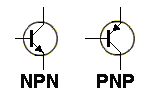
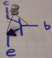
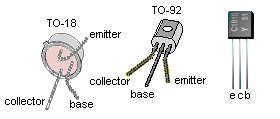
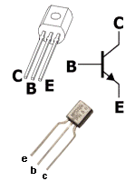
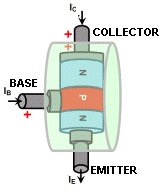
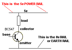
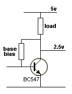
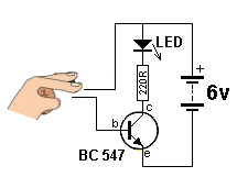
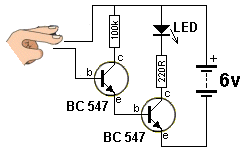
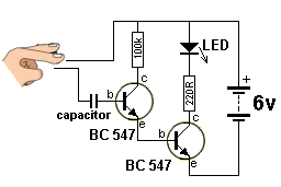
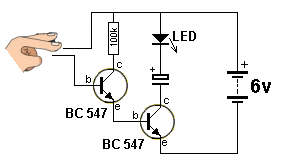
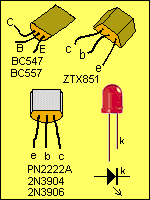
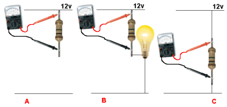
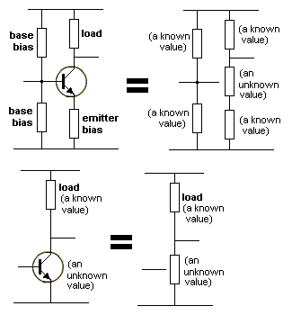
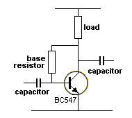
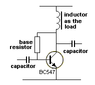
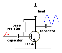
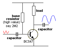
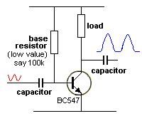
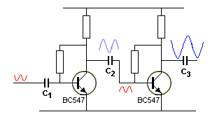
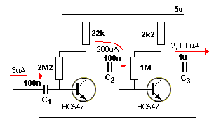
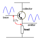
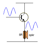
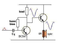
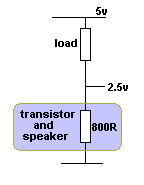
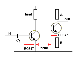
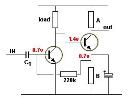
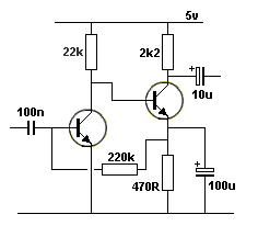
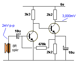
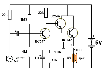
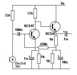
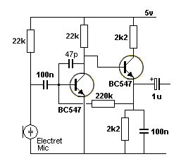
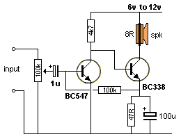
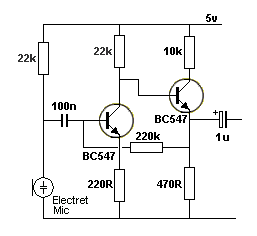
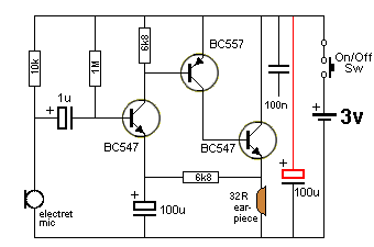
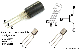
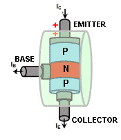
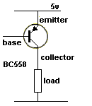
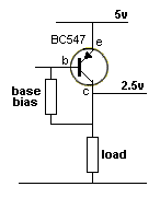
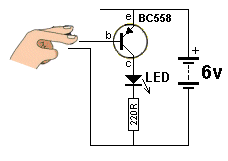
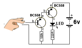
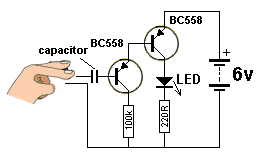
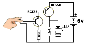
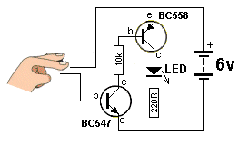
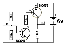
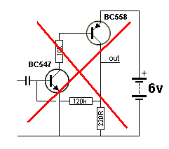
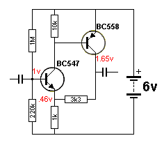
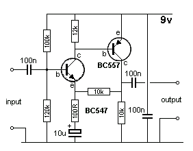
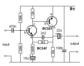
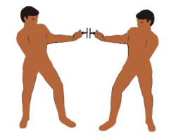

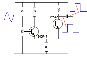
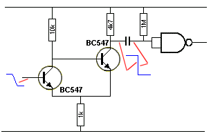
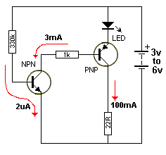
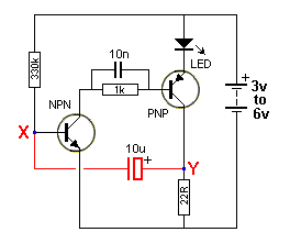
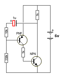

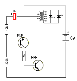
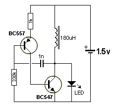
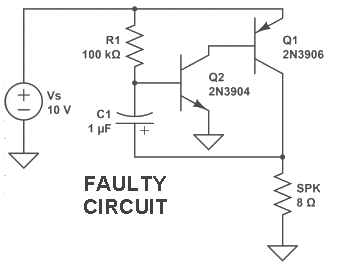
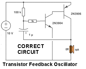
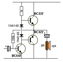
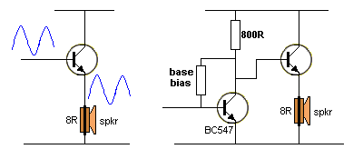
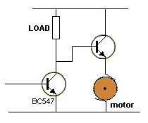
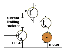
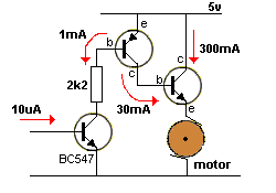
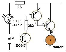
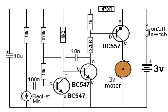
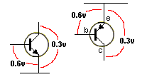
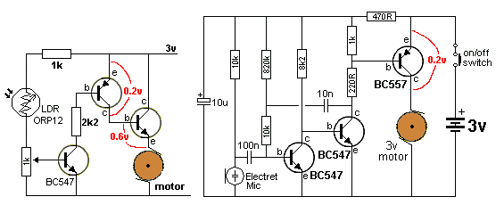
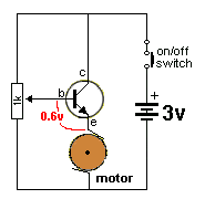
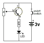
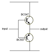
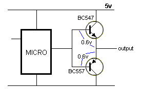
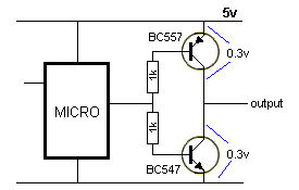
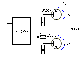
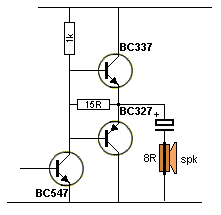
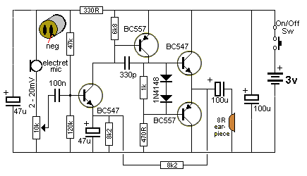
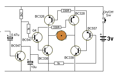
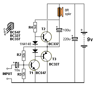
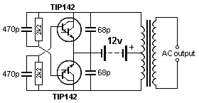
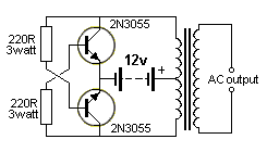
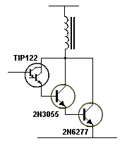
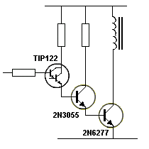
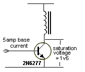
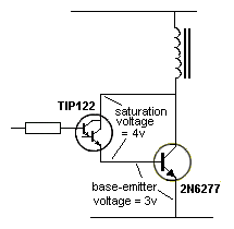
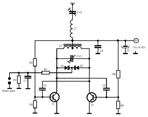
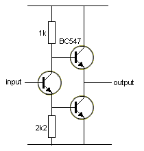
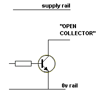
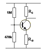
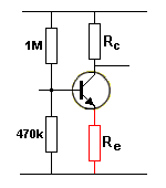
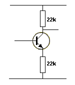
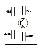
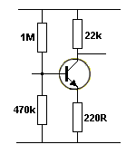
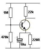
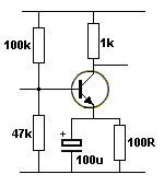
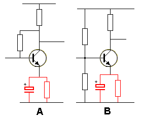
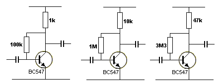
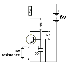
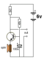
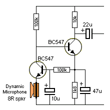
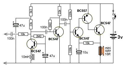
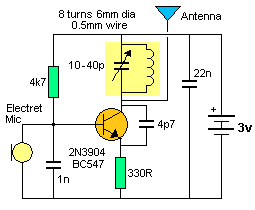
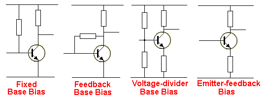
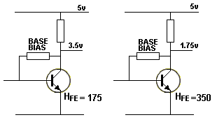
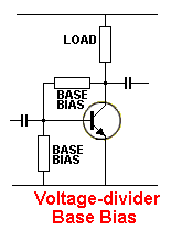
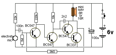
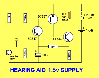
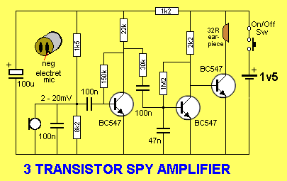
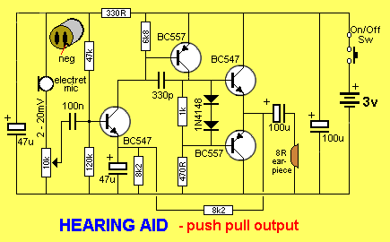
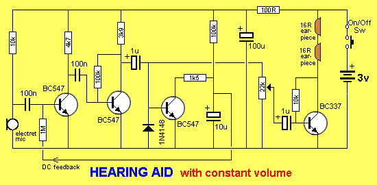
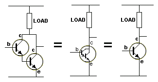
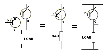
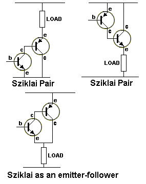
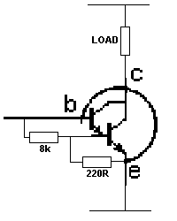
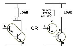
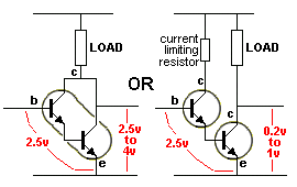
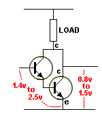
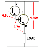
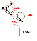
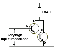
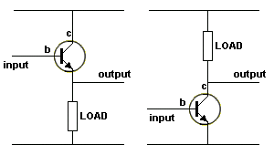
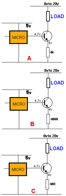
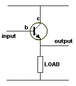
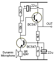
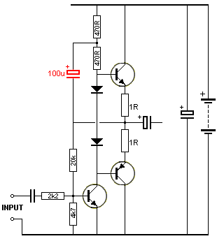
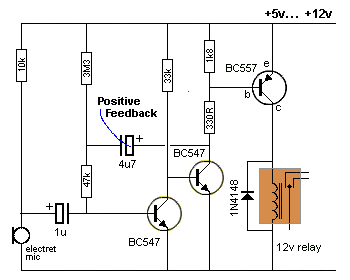
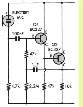 It
is exactly the same circuit as Fig 71acc above, but
"up-side-down."
It
is exactly the same circuit as Fig 71acc above, but
"up-side-down."