|

A "Stage"
Blocking Oscillator
Bridge - the
Bootstrap Circuit
Colpitts Oscillator
Common Base Amplifier
Connecting 2 Stages
Constant Current Circuit - the
Coupling Capacitor - the
Current
Darlington - and the Sziklai Pair
Differential Amplifier
Digial Stage - the
Hartley Oscillator
Impedance Maching
Long Tailed Pair
NPN Transistor
NPN/PNP Amplifier
Oscillators Oscillators
Phase-Shift Oscillator
PNP Transistor
Schmitt Trigger - the
Sinewave Oscillator
Sinking and Sourcing
Square Wave Oscillator
Stage Gain
1 watt LED - driving a high-power LED
THE FET
The Field-Effect Transistor is
just like the ordinary transistors we have studied.
It has three leads and is connected just like an ordinary transistor.
The only difference is the name of the leads and the voltage on the
"base."
The "base" is now called the "GATE" and nothing happens on the GATE
until a higher voltage is reached.
The voltage on the BASE of an ordinary transistor needs to be 0.55v
before the transistor starts to conduct and at 0.7v it is
fully turned ON (can be up to 0.9v).
For a FET, the voltage on the GATE is HIGHER. It needs to be 3.5v for some FETs and
as high as 6v for others.
There are two other slight differences between a FET and an ordinary
transistor:
The voltage on a FET does not need any current. For an ordinary
transistor, CURRENT is needed into the base and the transistor will
amplify this about 100 - 200 times to produce collector current.
Since NO CURRENT is needed on the GATE of a FET,
the current through the source-drain can be as high as the device will
allow. This is the first advantage of a FET.
There is a very small "gap" or "range" where the voltage on the GATE
starts to turn the FET ON (from zero output current; gradually,
to full output current) and if you work in this range, the FET becomes an
audio amplifying device - linear amplifying device.
Every FET is different and the voltage range is quite considerable.
Refer to the following data sheet. The red frames contain the data for
the voltage on the gate to turn the FET on. These voltages are only a
guide and you need to build a circuit and test the device to determine
the actual values:
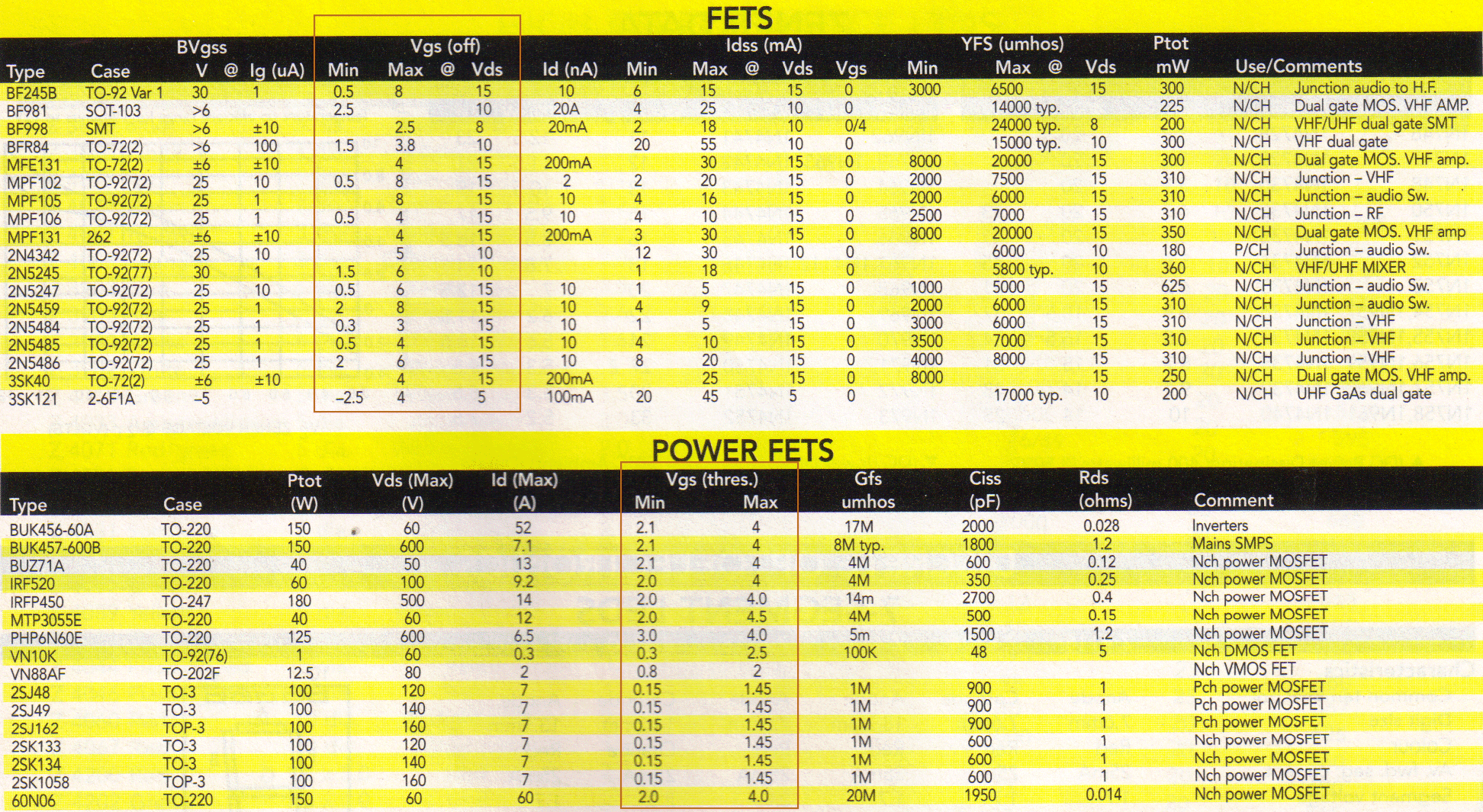
click image for enlarged view
However the FET has high losses when operating in this linear mode and the current it can
handle is limited.
When a FET is used in SWITCHING MODE (called Digital Mode) the losses in
the FET are minimal and the device can handle very high currents.
The second advantage is the voltage-drop across the DRAIN-SOURCE
terminals is very low and this means very little heat is generated
(lost) in the device and they can deliver (handle) a very high current.
If you think of a FET along these lines, you will not be "mystified."
(If you can achieve the relatively high input voltage needed, you can
use a FET.)
Here is a more-technical description of a
FET:
The Field-Effect Transistor provides an excellent voltage gain
with the added feature of a high input impedance. There are also
low-power-consumption configurations with good frequency range and
minimal size. JFETs, depletion MOSFETs, and MESFETs can be
used to design amplifiers having similar voltage gains. The depletion
MOSFET (MESFET) circuit has a much higher input impedance than
a similar JFET configuration.
Whereas a BJT device controls a large output (collector) current by
means of a relatively small input (base) current, the FET device
controls an output (drain) current by means of a small input
(gate-voltage) voltage. In general, therefore, the BJT is a current-controlled device
and the FET is a voltage-controlled device.
In both cases, however, the output current is the controlled
variable. Because of the high input characteristic of FETs, the ac
equivalent model is somewhat simpler than that employed for BJTs.
Whereas the BJT has an amplification factor,
b (beta),
the FET has a transconductance factor gm.
The FET can be used as a linear amplifier or as a digital device in
logic circuits. In fact, the enhancement MOSFET is quite popular in
digital circuitry, especially in CMOS circuits that require very low
power consumption. FET devices are also widely used in high-frequency
applications and in buffering (interfacing) applications. Although the common-source configuration is the most popular,
providing an inverted, amplified signal, common-drain (source-follower)
circuits providing unity gain with no inversion and common-gate circuits
providing gain with no inversion. Due to the
very high input impedance, the input current is generally assumed to be
0µA
and the current gain is an undefined quantity. Whereas the voltage gain
of an FET amplifier is generally less than that obtained using a BJT
amplifier, the FET amplifier provides a much higher input impedance than
that of a BJT configuration. Output impedance values are comparable for
both BJT and FET devices. A MOSFET is a transistor. It
is a Metal Oxide Field Effect Transistor.
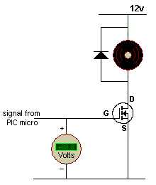
Here is an animation showing how to turn
on an N-channel MOSFET:
The easiest way to understand how MOSFETs
work is to compare them with PNP and NPN transistors and show them in
similar circuits. The advantage of a MOSFET is this: It requires
very little current (almost zero current) into the gate to turn it ON
and it can deliver 10 to 50 amps or more to a load.
A zener must be added to the gate of a
MOSFET if the gate voltage comes from a supply that is above 20v.
When the gate voltage is 4v LOWER than
rail voltage, the MOSFET turns ON. The 10k resistor on the base of the
transistor is needed to prevent the base current exceeding the amount of
current needed by the transistor to deliver current to the load. However
the 10k resistor on the gate of the MOSFET is not needed. Providing the
voltage (up to 18v) on the gate rises and falls quickly, the MOSFET will
not get hot. The critical period of time is the 0v to 3v section of the
waveform as this is when the MOSFET is turning on.
The solution is shown in the diagram below.
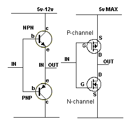
The transistor configuration will work on ANY rail voltage but the
MOSFET "totem-pole configuration" will only work up to 5v. This is due
to the characteristics of a MOSFET. The MOSFETs used in this arrangement
have a gate-to-source characteristic of slightly more than 3v and do not
turn on when the voltage across these two terminals is 3v. This means
the supply can be 6v and when the input is at mid-rail, 3v will be
across each gate-to-source and neither will be turned on. That's
why TTL logic is limited to 5v operation. The output will be extremely
close to rail-to-rail for the MOSFET configuration.
For a supply greater than 5v, a different MOSFET configuration must
be used to get full rail-to-rail output. The MOSFETs must be turned on
individually.
PUSH PULL USING MOSFETS
The circuit above is much more complex than
meets the eye.
Here is an audio amplifier using PUSH PULL mode to drive a speaker:
The top two transistors are in push-pull mode to turn the P-channel
MOSFET on and off very quickly. They speed up the incoming waveform and
prevent the MOSFET generating heat during the turning-on process.
Input A HIGH, Input D HIGH - forward
rotation
PWM MOTOR SPEED CONTROLLER
MOSFETs have very little tolerance to over-voltage. Damage to
devices may result even if the voltage rating is exceeded for as
little as a few nanoseconds. MOSFET devices should be rated
conservatively for the anticipated voltage levels and careful
attention should be paid to suppressing any voltage spikes or
ringing. High average current causes considerable thermal dissipation in
MOSFET devices even though the on-resistance is relatively low. If the
current is very high and heatsinking is poor, the device can be
destroyed by excessive temperature rise. MOSFET devices can be
paralleled directly to share high load currents. Massive current overload, even for short duration, can cause
progressive damage to the device with little noticeable temperature
rise prior to failure. If the control signals to two opposing MOSFETs overlap, a
situation can occur where both MOSFETs are switched on together.
This effectively short-circuits the supply and is known as a
shoot-through condition. If this occurs, the supply decoupling
capacitor is discharged rapidly through both devices every time a
switching transition occurs. This results in very short but
incredibly intense current pulses through both switching devices. When switching current through any inductive load (such as a
Tesla Coil) a back EMF is produced when the current is turned off.
It is essential to provide a path for this current to free-wheel in
the time when the switching device is not conducting the load current. A high Q resonant circuit such as a Tesla Coil is capable of
storing considerable energy in its inductance and self capacitance.
Under certain tuning conditions, this causes the current to
"free-wheel" through the internal body diodes of the MOSFET device. This behaviour is not a problem in itself, but a problem
arises due to
the slow turn-off (or reverse recovery) of the internal body diode. MOSFET body diodes generally have a long reverse recovery time
compared to the performance of the MOSFET itself. If the MOSFET gate is driven with too high a voltage, then the
gate oxide insulation can be punctured rendering the device useless.
Gate-source voltages in excess of +/- 15 volts are likely to cause
damage to the gate insulation and lead to failure. Care should be
taken to ensure that the gate drive signal is free from any narrow
voltage spikes that could exceed the maximum allowable gate voltage. MOSFET devices are only capable of switching large amounts of
power because they are designed to dissipate minimal power when they
are turned on. It is the responsibility of the designer to ensure
that the MOSFET device is turned hard on to minimise dissipation
during conduction. If the device is not fully turned on then the
device will have a high resistance during conduction and will
dissipate considerable power as heat. A gate voltage of between 10
and 15 volts ensures full turn-on with most MOSFET devices. Little energy is dissipated during the steady on and off states,
but considerable energy is dissipated during the times of a
transition. Therefore it is desirable to switch between states as
quickly as possible to minimise power dissipation during switching.
Since the MOSFET gate appears capacitive, it requires considerable
current pulses in order to charge and discharge the gate in a few
tens of nano-seconds. Peak gate currents can be as high as 1 amp. MOSFETs are capable of switching large amounts of current in
incredibly short times. Their inputs are also relatively high
impedance, which can lead to stability problems. Under certain
conditions high voltage MOSFET devices can oscillate at very high
frequencies due to stray inductance and capacitance in the
surrounding circuit. (Frequencies usually in the low MHz.) This
behaviour is highly undesirable since it occurs due to linear
operation, and represents a high dissipation condition. MOSFET devices have considerable "Miller capacitance" between
their gate and drain terminals. In low voltage or slow switching
applications this gate-drain capacitance is rarely a concern,
however it can cause problems when high voltages are switched
quickly. A potential problem occurs when the drain voltage of the bottom
device rises very quickly due to turn on of the top MOSFET. This
high rate of rise of voltage couples capacitively to the gate of the
MOSFET via the Miller capacitance. This can cause the gate voltage
of the MOSFET to rise resulting in turn on of this device as
well ! A shoot-through condition exists and MOSFET failure is
certain if not immediate. Rapid switching of large currents can cause voltage dips and
transient spikes on the power supply rails. If one or more supply
rails are common to the power and control electronics, then
interference can be conducted to the control circuitry. Antistatic handling precautions should be used to prevent gate
oxide damage when installing MOSFET or IGBT devices.
But are very reliable once they are
soldered in place.
This is just a start to learning about transistor circuits and more can
be found on Talking
Electronics website.
24/8/2011 - constantly being updated and added-to
Here are the symbols for FETs and MOSFETs: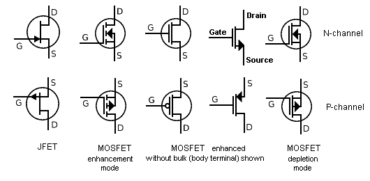
MOSFET turns ON when
gate-to-source
is more than about 2v (2v to 5v)
A MOSFET can be used in place of an ordinary transistor (called a
bipolar junction transistor, or BJT) providing one slight difference is
taken into account.
An ordinary NPN transistor will turn ON when the base voltage is about
0.65v more than the emitter but a MOSFET needs the gate terminal to be
at least 2v to 5v, (depending on the type of MOSFET) above the source
voltage.
Here is a comparison between an NPN transistor and N-channel MOSFET: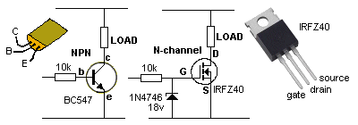
A normal transistor is a current amplifying device.
For a load current of 100mA, the base current for a BC547 will need to
be about 1mA.
This means it has a current gain of about 100.
A MOSFET is a voltage controlled device and the current it will handle
depends on its physical size and the way it is constructed. You cannot
change this parameter.
For a load current up to about 35Amp, the gate current for a IRZ40 will
be less than 0.25mA. When the gate voltage is 3v to 4v higher than the
source, it turns on and the resistance between source and drain
terminals is about 0.028 ohms. It will handle up to 35 amps.
The load determines the current through the MOSFET (not the MOSFET) and
if it is less than 35 amps, a IRFZ40 is suitable for the application.
Comparison between a PNP transistor and P-channel MOSFET: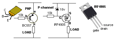
PUSH PULL
MOSFETs can be placed in push-pull mode,
just like PNP and NPN transistors.
They must be connected correctly to prevent damage.
In the following circuit you can see the transistors and MOSFETs have
been connected incorrectly.
For the PNP/NPN transistor circuit, as the input changes from high to low
or low to high, both transistors are turned on during the transition.
Only one transistor is turned on when the line is high and only the
other
transistor is turned on when the line is low, but during the transition,
BOTH are turned on.
The same applies with the MOSFETs. When the input is at mid-rail, a
voltage between gate and source will be produced for both MOSFETs. Since
a MOSFET can handle many amps, this will put a short-circuit across the
power rail and will cause a lot of damage. 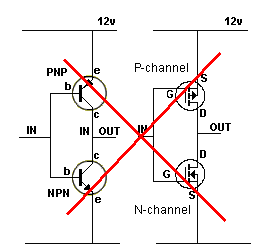
Transistors and MOSFETs
will produce short-circuit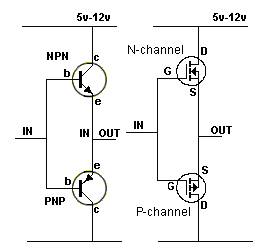
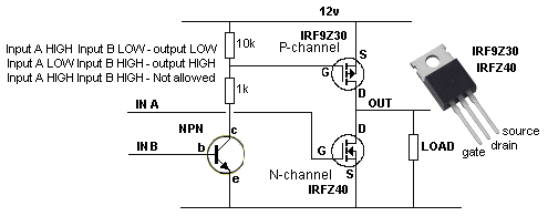
The circuit above sinks up to 35A via the N-channel MOSFET and delivers
about 18Amp via the P-channel MOSFET. Input A must rise quickly
to prevent the MOSFET heating up during the turning-on period. Input
A must rise to at least 4v to guarantee the MOSFET turns ON.
Input B must rise above 0.65v to turn the transistor ON. The
voltage on the collector of the transistor will fall and this will
provide a gate-to-source voltage for the P-channel MOSFET.
Both inputs must not be HIGH at the same time as this will turn ON both
MOSFETs and create a short-circuit on the power rail.
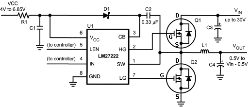
To turn on the top N-channel MOSFET, the gate must be taken at least 3v
higher than the source because it is a SOURCE FOLLOWER (similar to an
EMITTER FOLLOWER). This is equal to Vin + 3v.
How does pin HG get this high voltage?
It gets it from a voltage doubling circuit made up of the 0.33u, high
speed diode D1 and an oscillator in the chip.
The circuit is a buck converter and will reduce any supply voltage to a
lower voltage with very high efficiency. It allows a small "packet of
energy" to flow to the Vout terminal via the inductor L1 and this
percentage determines the Vout voltage. 
The two lower transistors do the same thing.
The diodes and resistors connected to the input form a voltage-divider
to correctly bias the push-pull transistors.
H-BRIDGE
An H-Bridge can be designed using MOSFETs: 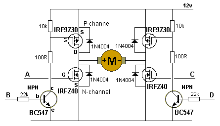
Input B HIGH, Input C HIGH - reverse rotation
Input A HIGH, Input B HIGH - not allowed
Input C HIGH, Input D HIGH - not allowed
The H-Bridge can be designed with two more transistors so that only two
input lines are needed.
Here is a circuit from a 12v drill. The MOSFET will deliver up to
30Amps.
The frequency of the oscillator is in the range 550Hz to
about 6.5kHz, with an off period of about 2.6us.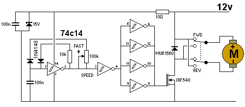
PWM 12v CORDLESS DRILL MOTOR
CONTROLLER
WHY MOSFETs FAIL
There are quite a few possible causes for device
failures, here are a few of the most important reasons:
The chances of shoot-through occurring are minimised by allowing a
dead time between switching transitions, during which neither MOSFET
is turned on. This allows time for one device to turn off before the
opposite device is turned on.
This current is usually directed through a free-wheel diode connected anti-parallel with
the
switching device. When a MOSFET is employed as the switching
device, the designer gets the free-wheel diode "for free" in the
form of the MOSFETs intrinsic body diode. This solves one problem,
but creates a whole new one...
This problem is usually eased by the addition of a high speed (fast recovery) diode. This ensures that the MOSFET body diode is never driven into
conduction. The free-wheel current is handled by the fast recovery
diode which presents less of a "shoot-through" problem.
Spurious oscillation can be prevented by minimising stray
inductance and capacitance around the MOSFETs. A low impedance
gate-drive circuit should also be used to prevent stray signals from
coupling to the gate of the device.
The Miller effect can be minimised by using a low impedance gate
drive which clamps the gate voltage to 0 volts when in the off
state. This reduces the effect of any spikes coupled from the drain.
Further protection can be gained by applying a negative voltage to
the gate during the off state. eg. applying -10 volts to the gate
would require over 12 volts of noise in order to risk turning on a
MOSFET that is meant to be turned off !
Good decoupling, and star-point earthing are techniques which
should be employed to reduce the effects of conducted interference.
The author has also found transformer coupling to drive the MOSFETs
very effective at preventing electrical noise from being conducted
back to the controller.
For a mathematical approach to understanding
the operation of a FET and some further circuits, here are four
documents:
The FET .pdf 670KB
The FET Amplifier .pdf
310KB
MOSFET Basics .pdf
380KB
FET Principles and Circuits .pdf 1MB
We have avoided mathematics and theory for a reason. Transistors have
such wide parameters that theoretical values and "Computer models"
do not work.
Most circuits have to be built and tested using transistors from
different manufacturers to be sure they work every time. The author had a batch
of transistors from a different manufacturer for his FM transmitters and
THEY DID NOT WORK.
The gain at 100MHz was so poor, the FM Bug did not transmit.
The only way to learn is by "building circuits." Text books
don't do this. Show me a text book that explains the output current for a
common-emitter stage is dependent on the LOAD resistor (in the circuits
above).
Show me a book that explains why capacitor-coupling two stages is
so inefficient.
Or why the load resistor in Fig 25 should be 15 ohms and not 330 ohms.
You can get too tied up in mathematics and theory and as the saying goes:
"You can't see the wood - (forest) - for the trees."
You have to be able to look at a circuit and see things "going up and
down" or "passing energy from one stage to the next." And that's what we have tried to do.
email Colin Mitchell
for any extra theory you want added.