|
TOPICS:
Adjustable Current Power Supply
Adjusting The Stage Gain
AF Detector
ANALOGUE and DIGITAL mode Read this section to see what we mean
Analogue To Digital
AND Gate
A "Stage"
Back EMF
Base Bias
Base-emitter Voltage
Biasing A Transistor
Biasing Diodes in push Pull Amplifier
Biasing the base
Blocking Oscillator
Bridge - the
Boost Converter
Bootstrap Circuit
Breakdown - Transistor Breakdown
Buck Converter - the
Buffer - The Transistor Buffer
Capacitor - The Capacitor passing a spike or signal - How the capacitor works
Capacitor Coupling
CFL Driver - flyback Oscillator
Changing A Transistor
Class-A -B and -C
Clipping and Distortion
Collector Open
Colpitts Oscillator
Common Base Amplifier
Common Collector - Emitter Follower
Common-Collector Problems
Configurations - summary of features of Common Emitter, C-Collector, and Common Base
Common Emitter with Self-Bias - base-bias resistor produces negative feedback
Common Emitter stage with fixed base bias
Connecting 2 Stages
Constant Current Circuit - the
Constant Voltage Circuit - the
Coupling Capacitor - the
Courses available - see discussion at end of this topic: Designing An Output Stage
Current
Current gain of emitter follower stage
Current Buffer Circuit
Current Limiter Current Limited Power Supply
Current to Voltage Converter
Current Mirror Circuit
Darlington - and the Sziklai Pair
Decoupling
Designing an Output Stage
Design Values
Design Your Own Transistor Amplifier
Differential Amplifier
Differentiation
Digital Stage - the
Digital Transistor - the
Diode Pump - The - How the DIODE works
Distortion for Guitar
Drive a Relay - constant current driving
Driver Stage - the
Distortion and Clipping
Efficiency of a coupling capacitor . . . . 8%!!
Electronic Filter
EMF Back EMF
Emitter by-pass capacitor
Emitter Capacitor
Emitter Degeneration - or Emitter Feedback
Emitter Follower
Emitter Resistor - and emitter capacitor
Feedback Capacitor
Feedback - positive
Filters
FlyBack Oscillator FlyBack Oscillator
Fuzz
Gain
Gates
Guitar pre-amplifier
Hartley Oscillator
High Current Driver - faulty design
Higher Gain Using A Transistor with a Higher or Lower Gain
High Input Impedance Circuit
High-Pass Filter
High-side Switching
How an Oscillator Starts
Hysteresis
Illuminating a globe (lamp)
Impedance Matching
Increasing mobile handset volume
Input and Output Impedance
Integration and Differentiation
Interfacing
Inverter - transistor as an
Latch Circuit
Leakage - the small leakage current due to combining two or more transistors
Level Conversion or LEVEL SHIFTING see also Level Shifting via an Inverter
Lighting a globe (lamp)
Linear Amplifier Transistor as a
Long Tailed Pair
Low Impedance Circuit
Low-Pass Filter
Low-side Switching
Motor-boating
NAND Gate
Negative feedback - lots of circuits have negative feedback. See Fig 103cc
Negative Feedback
Negative Voltage
No Current - a circuit that takes no current when "sitting around."
NPN Transistor
NPN/PNP Amplifier
Open Collector
Oscillator How it starts
Oscillators Oscillators
Output Stage - Designing
Pass Transistor
Phase-Shift Oscillator
PNP Transistor
Positive Feedback. See Fig 103cc
Potentiometer - The
Power of a SIGNAL
Pull-Up and Pull-Down Resistors
Push Pull
Programmable Unijunction Transistor (PUT)
Regulator - transistor
Relay - driving a relay
Saturating a Transistor
Schmitt Trigger - the
SCR made with transistors
"Shoot-Through" Current
Short-Circuit Current
Signal driving power
Sinewave Oscillator
Sinking and Sourcing
Split Supply - Split Power Supply
Square Wave Oscillator
Square-wave to Sinewave
Switch - The transistor as a Switch
Stage Gain
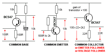
Summary of a transistor connected in common-emitter, common-base and common-collector
Super-Alpha Circuit
Sziklai Pair
Thyristor (scr) made with transistors
Time Delay
Totem Pole Stage
Transformer - adding a transformer
Transistor as a LOAD
Transistor as a Variable Resistor
Transistor Replaces Relay
Transistor Tester
Transistors with Internal Resistors
Tri-State
Twin T Oscillator
UniJunction Transistor
Voice Operated Switch - see VOX
Voltage Amplifier Circuit
Voltage Buffer Circuit
Voltage Divider
Voltage Doubler - the
Voltage to Current Converter
Voltage Regulator
Voltages - measuring Voltages
VOX - Voice Operated Switch
Zener Tester - How the ZENER DIODE works
Zener The transistor as a zener Regulator
1 watt LED - driving a high-power LED
12v CFL Driver - Flyback Circuit
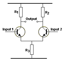
THE DIFFERENTIAL AMPLIFIER
or
LONG TAILED PAIR
|
|
The DIFFERENTIAL AMPLIFIER is also
called the "Difference Amplifier" or long-tailed pair
(LTP), or emitter-coupled pair, because it
amplifies the difference between the voltages on Input 1 and
Input 2. It is called a Long Tailed Pair because the
emitter resistor has a high value. The circuit has the advantage
of ONLY amplifying the signals on the Inputs. Any noise on the
power rail is not detected on the output as both transistors
will see this fluctuation and both outputs will either rise
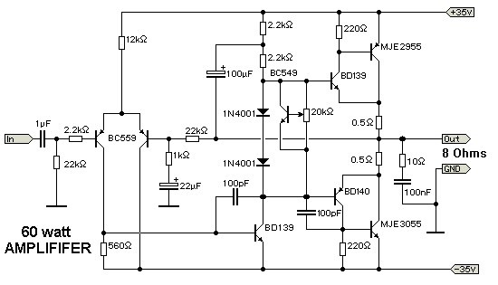
or fall and thus the output will not change. Since the Long Tailed Pair does not pick up noise from the supply, it is ideal as a pre-amplifier as shown in the 60 watt amplifier in Fig 71ae: |
|
|
|
|
|
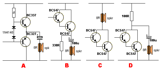
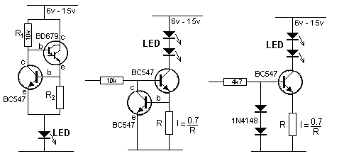
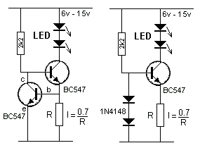
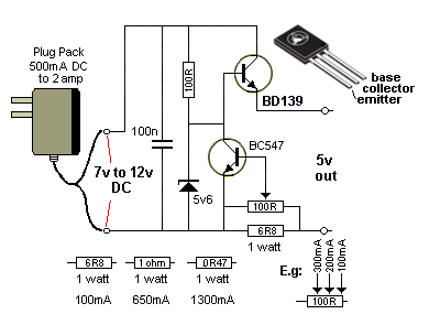
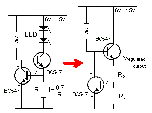
| The three circuits above provide a constant current through the LED (or LEDs) when the supply rises to 15v and higher. The second and third circuits can be turned on and off via the input line. |
|
|
The first circuit in
Fig 71b is a constant-current arrangement,
providing a fixed current to the LEDs, no matter the supply
voltage. This is done by turning on the top transistor via the 2k2 resistor. It keeps turning on until the voltage-drop across resistor R is 0.65v. At this point the lower transistor starts to turn on and current flows through the collector-emitter terminals and it "robs" the top transistor of current from the 2k2 resistor. The top transistor cannot turn on any more and the current flowing though R is the same as the current flowing through the LEDs and does not increase. |
|
The second diagram in Fig 71b is also a constant-current circuit
with the base fixed at: |
|
|
Fig 71ba shows two more constant current circuits "sourcing" the LEDs. The 7 constant current circuits give you the choice of either sourcing or sinking the LED current. |

|
|
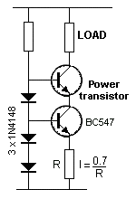
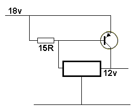
If the supply voltage is high, the transistor
controlling the current (BC547) will get hot and alter the
current-flow. Fig 71bab uses a POWER TRANSISTOR to dissipate the losses and the current-controlling transistor remains cold. When the circuit turns ON, the current through R is zero and the voltage on the base of the BC547 turns it on fully. The voltage between collector and emitter is about 0.2v and this means the emitter of the power transistor is below the base of the BC547. The base of the power transistor is 0.7v above the base of the BC547 and the power transistor also turns on fully. Current increases through R and when the voltage across R reaches 0.7v, The BC547 starts to turn OFF. The collector voltage rises and this starts to turn OFF the power transistor. This is how the current through the LOAD is limited by the value of R. |
|
|
A CONSTANT VOLTAGE circuit is simply a POWER
SUPPLY. Provided the input voltage is at least 3v higher than the output voltage and it is capable of supplying the required current, the output voltage will remain constant at the voltage determined by the setting of the pot. |
|
|
This is not a constant current circuit. It
is a CURRENT SOURCE circuit. A constant current
circuit means the current will not change if the supply voltage is
increased or decreased. This circuit simply supplies a DC signal (in the
form of a voltage) to another circuit so that the current in the
original circuit is available in the second circuit and this is called a
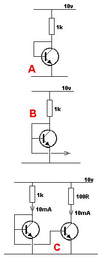
current mirror arrangement. We start with diagram A. The transistor is turned on because the base is connected to the collector. The collector can only rise to about 0.7v because it is connected to the base so that most of the supply-voltage appears across the load. This means the current through the load is known. It can be determined by Ohm's Law: I =V/R. Here's how the circuit works: When the circuit is turned ON, current flows through the resistor and through the base-emitter junction. This turns the transistor ON very hard and the current through the collector-emitter circuit increases. This reduces the voltage on the collector and as it decreases, the voltage on the base decreases and the transistor starts to turn OFF. In the end, the transistor is turned on to allow 10mA to flow through the collector-emitter junction due to the 10v supply and 1k resistor. Suppose we instantly change the 1k for 100 ohms. The transistor is only lightly turned ON and current though the collector-emitter is only 10mA. But the 100R will deliver 100mA and the extra current will flow into the base and turn the transistor ON harder. This will increase the current thorough the collector-emitter junction and rob the base of the extra current, however the current into the base will be higher than before because the transistor has to be turned on more to allow about 100mA to flow through the collector-emitter junction. If we take a lead from the base of the transistor, as shown in fig B we can connect it to the base of an identical transistor and the second transistor will allow the same current to flow though the collector-emitter junction. The result is circuit C. The current through the 100R resistor will be 10mA (normally it would be 100mA). The second transistor is only lightly turned on and allows 10mA to flow. |
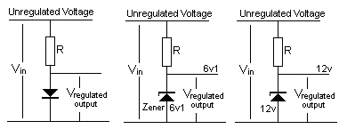
| Before we go to the
2-transistor Voltage Regulator, we will
explain how a voltage regulator works. The basis of all voltage regulators is a diode. A diode has a voltage characteristic. When a voltage is placed across its terminals, and the voltage starts at zero, no current flows through the diode until the voltage reaches 0.65v. As soon as it reaches 0.65v, current flows and as you increase the voltage, more current flows but the voltage across the diode remains at 0.65v. If the voltage is increased further, the current increases enormously and the diode will be destroyed. This characteristic does not apply to a resistor. The voltage across a resistor will increase when the supply voltage increases and thus a resistor cannot be used as a Voltage Regulator. We have selected 0.65v for this discussion as this is the characteristic voltage-drop for a normal silicon diode. However germanium diodes and Schottky diodes have different characteristic voltage drops. On top of this, special diodes can be produced with higher voltages. These are called ZENER DIODES. They all have the same characteristic. As soon as the specified voltage appears across the terminals of the diode, current starts to flow and if the voltage is increased too much, the diode will be damaged. To prevent this, a resistor must be placed in series with the diode. This is the basis of all voltage regulators. |
|
|
|
|
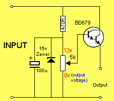
| In Fig 71be, the supply voltage is called the
UNREGULATED VOLTAGE and it is connected to resistor R and
a diode. The voltage at the top of the diode is called the
REGULATED VOLTAGE. The diode produces a fixed 0.65v and
the zener produces a fixed 6v1 or 12v. This circuit is called a SHUNT REGULATOR because the regulator is shunted (placed across) the load. [A Shunt is a load - generally a low-value resistor - placed across a component in a circuit to take a high current to either protect the other components or to test the circuit under high-current conditions.] That's exactly what the diode or zener diode does. It takes ALL THE CURRENT from the unregulated supply and and feeds it to the 0v rail. During this condition the circuit is 100% wasteful. All the wattage is being lost in heating resistor R and heating the diode. The circuit is providing a fixed voltage at the top of the zener. When a load is added to the circuit, it takes (or draws) current and this current comes from the current flowing though the zener. The load-current can increase to a point where it takes nearly all the current from the zener. If it takes more current than the zener, two things happen. Current stops flowing though the zener and the voltage on the top of the zener drops to a lower value. This is the point where the zener has dropped out of regulation and the circuit is no longer regulating. In other words: A current is flowing into the regulator circuit and it is being divided into two paths: The zener path and the load path. The load path cannot be more than 95% or the regulator will drop out of regulation (the output voltage goes below the zener voltage). Here's how the diode (or the zener) works: The zener is just like a bucket with a large hole in the side. As you fill the bucket, the water (the voltage ) rises until it reaches the hole. It then flows out the hole (through the zener) and does not rise any further. When you draw current from the circuit it is the same as a tap at the bottom of the bucket and the water flows out the tap and not the hole. The pressure out the tap is the voltage of the zener. The only disadvantage of this circuit is the voltage across the zener changes a small amount when the current through it changes. The SHUNT REGULATOR is limited to small currents due to the fact that the load is taking the current from the zener. The current can be increased by adding a buffer transistor to produce a BUFFERED SHUNT REGULATOR as shown in Fig 71bf. This circuit actually becomes a PASS TRANSISTOR arrangement.
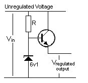
See more circuits on the Zener Regulator and the Transistor Shunt Regulator and Pass Transistor Regulator in 101-200 Transistor Circuits. A very clever circuit to reduce ripple is called the Electronic Filter. 00000000000000000000000000000 The whole concept of a regulator (removing the ripple while maintaining the required voltage) revolves around the voltage-drop across a diode and in Fig 71bb, the diode is replaced with the voltage-drop across the base-emitter junction of a transistor. This voltage-drop is fairly constant when a small current flows and this is the basis of the Two Transistor Regulator: |
|
|
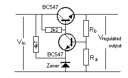
If we take the Constant-Current Circuit shown in
Fig 71b above, and split resistor R into Ra and Rb,
we produce an identical circuit with a completely different name. It
is called a TWO TRANSISTOR REGULATOR. The circuit will produce a smooth voltage on the output, even though the rail voltage fluctuates AND even if the current required by the output increases and decreases. That's why it is called a REGULATOR CIRCUIT. The current through Ra and Rb is "wasted current" so it does not have to be more than 1mA - enough to turn on the lower NPN transistor. Ra and Rb form a voltage divider and when the join of the two resistor reaches 0.7v, the lower transistor turns ON. |
|
| The
lower transistor forms a voltage-divider with the 2k2 to pull the
top BC547 transistor DOWN so the voltage
on the output is kept at the "design voltage" (the top transistor is
an emitter follower). If the device connected to the output requires
more current, the top transistor will not be able to provide it and
the output voltage will drop. This will reduce the voltage on the
base of the lower transistor and it will turn OFF slightly. The voltage on the base of the top transistor will rise and since this transistor is an emitter-follower, the emitter will rise too and increase the output voltage to the original "design value." Regulation is also maintained if the supply decreases (or increases). If the supply decreases, the voltage on the base of the top transistor will fall and the output voltage will also fall. The voltage on the base of the lower transistor will also fall and it will turn off slightly. This will increase the voltage on the base of the top transistor and Vregulated will rise to the design value. Both the supply and the load can change at the same time and the circuit will compensate. All we have to do is re-draw the circuit as a standard 2-Transistor Regulator as shown in Fig 71bc and you have covered the principle of its operation.
|
||
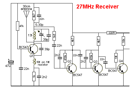
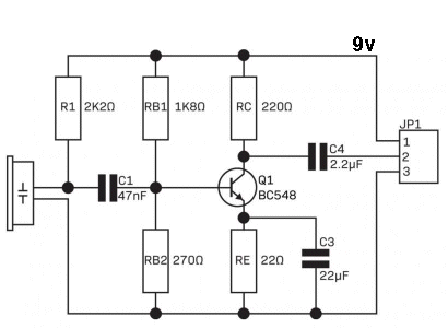
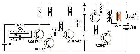
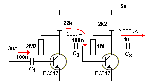
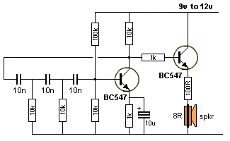
AND RF DETECTOR
A transistor can be used as a "detector" in a radio circuit. The Detector stage in a radio (such as an AM receiver), is usually a crystal, but can be the base-emitter junction of a transistor.
It detects the slowly rising and falling audio component of an RF signal. This signal is further amplified and delivered to a speaker. A single transistor will perform both "detection" and amplification.
In Fig 71bd, the first transistor provides these two functions and the output is passed to the second transistor via direct-coupling.
The first two transistors provide enormous gain and a very high input impedance for the tuned circuit made up of the 60t aerial coil and 415p tuning capacitor. The signal generated in the "tuned circuit" is prevented from "disappearing out the left end" by the presence of the 10n capacitor as it holds the left end rigid.
|
|
|
We have shown the coupling
capacitor transfers very little energy when it does not get
fully discharged during part of the cycle and this means it
cannot receive a lot of energy to charge it during the
"charging" part of the cycle.
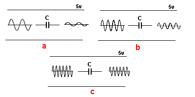
A 1u
capacitor at 200Hz is like putting a 1k resistor between one
stage and the next.
A
10u capacitor at 200Hz is like putting a 100R resistor between
one stage and the next and a 100u capacitor at 200Hz is like putting a 10R resistor between
one stage and the next.
In Fig 71d
you can see the "resistance" of a capacitor is very small
compared to the LOAD resistance (the main component that
determines the amount of energy that can be transferred from one
stage to another and the impedance of the receiving stage
- the component that determines the discharging of the
capacitor). The "resistance" of a capacitor decreases as the
frequency increases.
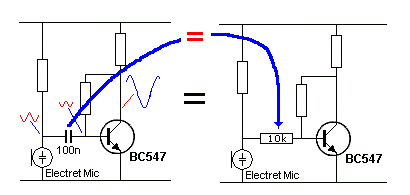
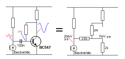
The waveform on the output of the electret microphone is 20mV
p-p (peak-to-peak).
This amplitude passes through the 100n capacitor, which we have
drawn as a 10k resistor, (to represent the capacitive reactance
of the capacitor at 200Hz). The input impedance of the
common-emitter amplifier is about 500 ohms to 2k. (500 ohms when
the base current is a maximum and 2k when the base current is
very small).
It is very difficult to work out
how much energy will be transferred by the capacitor coupling
the two stages in the circuit above. |
|
|
|
Fig 71g
shows each transistor stage has an input and output
impedance. This really means an input and output
resistance, but because we cannot measure the value with
a multimeter, we have to find the value of resistance by
measuring other things such as "waveform amplitudes" and
then create a value of resistance, we call IMPEDANCE.
The values shown are only approximate and apply to
transistors called SMALL SIGNAL DEVICES. The values are
really just a comparison to show how the different
stages "appear" to input and output devices, such as
when connecting stages together. The input impedance of a common-emitter stage ranges from 500R to 2k. This variation depends on the type of transistor and how much the stage is being turned ON. In other words, the amount of current entering the base. The value of 2k2 for the emitter-follower depends on the current entering the base. These values are all approximate and are just to give an idea of how to describe the various values of impedance. INPUT IMPEDANCE There are so many discussions in text books on the INPUT IMPEDANCE of a transistor and they are all complex and confusing for the beginner. Here is a simple explanation. The transistor is like a FORK-LIFT TRUCK. You move the lever UP and the fork lifts a pallet of bricks. The same with a transistor, you deliver a small current into the base and the collector delivers a higher current at the collector terminal. This higher current passes through a load (such as a resistor) placed between the collector and the positive rail. But a transistor can only amplify the current about 100 times. A fork-lift truck can amplify the lever about 10,000 times. So, don't worry about terms such as IMPEDANCE. All you have to remember is this: The transistor will amplify the current delivered to the base, about 100 times. Of course you also have to know how much current is being delivered to the base from a previous stage, but that is a problem for another time. When you place two transistors "on top of each other" to produce a "transistor" called a super-alpha transistor or DARLINGTON transistor, the first transistor amplifies the current by 100 and the second amplifies this current another 100 times, making a total of 100 x 100 = 10,000 and it is as strong as a fork-lift truck !! Because the first transistor is helping the second transistor, we also say the input impedance is increased by a factor of 100. But it really all boils down to the fact that the current capability is INCREASED. There are other facts such as voltage, and amplification will decrease as the current increases, but you can study this AFTER you realise the transistor is simply INCREASES THE CURRENT. |
Also called the TRANSISTOR TIME DELAY or TIME CONSTANT or RC Delay Circuit or TIMING CIRCUIT.
A Delay Circuit is made with a capacitor and resistor in series:
The TIME DELAY circuit
These are
the two components that create the TIME DELAY. No other parts
are needed. When the value of the capacitor and resistor
are multiplied together the result is called the TIME CONSTANT
and when the capacitor value is in FARADS and resistor in OHMs,
the result is SECONDS
HIGH FREQUENCY "NOISE"
To detect when the capacitor has reached about 63% of its final
voltage, we need some form of detecting device, such as a
transistor.
But the detecting device cannot "steal" any of the current
entering the capacitor, otherwise the voltage on the capacitor
will never increase or take longer to increase.
We know a transistor requires current for it to operate but a
Darlington Pair (or Darlington) requires very little current, so the
detecting device must be something like a Darlington.
The transistor plays no part in the timing (or TIME DELAY)
of the circuit. It is just a detector.
The main secret behind a good TIME DELAY circuit is to allow the capacitor
to charge to a high voltage and use a large timing resistor.
This reduces the size of the capacitor (electrolytic) and
produces a long time delay.
There are lots of chips (Integrated Circuit) especially
made for timing operations (time delays). Transistors (of the
"normal" type - called Bipolar Junction) are not suited for long
time delays.
Field Effect Transistors, Programmable Uni Junction transistors
and some other types are more suited.
However a normal transistor can be used, as shown in Fig 71h.
The normal detection-point is 63% but you can make the circuit
"trigger" at any voltage-level. The value "63%" has been chosen
because the voltage on the capacitor is increasing very little
(each second) when it is nearly fully charged and waiting for it
to reach 65% may take many seconds. Trying to detect an extra 10%
or 25% is very hard to do and since it takes a long time for the
voltage to rise, the circuit becomes very unreliable and very
inaccurate. That's why 63% has been chosen.
See also Integration and Differentiation.
The same two components (a resistor and capacitor) can be used for a
completely different purpose. That's the intrigue of electronics.
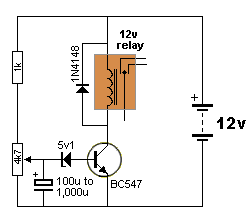
Fig 71h
Fig 71h shows
a TIME DELAY circuit. This circuit does not wait for the
capacitor to charge to 63% but it detects a voltage of 5v1 +
0.7v = 5v8.
The detecting circuit is made up of the 5v1 zener and
base-emitter junction of the transistor.
These two components create a high impedance until a voltage of
5v8 because the zener takes no current until its "characteristic
voltage" has been reached.
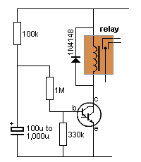
Fig 71j
Fig 71j shows
a Time Delay Circuit. The 100k is the time delay resistor. The
1M is the "sense resistor" and the the 330k is the voltage
divider resistor.
The base of the Darlington transistor detects 1.4v and the
1M/330k produces a voltage divider that requires 3 x 1.4v = 4.2v
on the electrolytic. The 1M, 330k and transistor provide a
fairly high impedance detecting circuit that does not inhibit
the charging of the capacitor.
The circuit requires a supply of 12v.
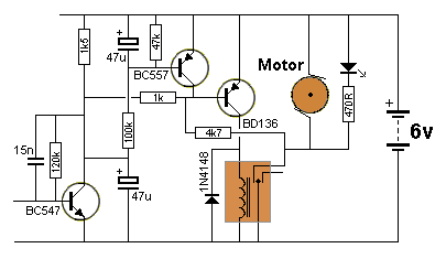
Fig 71
Fig 71k shows two Time Delay Circuits as well as a latching circuit
(the 4k7 resistor), a buffer transistor (BD136) and a high frequency filter (the 15n
capacitor).
When the circuit is turned ON, the relay is not energised. The
signal on the base of the first transistor has any high
frequency component removed by the 15n capacitor (see below for
the effect of a filter on a signal).
The lower 47u is fully charged via the 1k5 a very short time
after the circuit is turned on and the output of the first
transistor discharges this electrolytic very quickly when it
receives a signal.
This turns ON the BD136 transistor via the 1k resistor
and the relay is energised.
The output of the relay is connected to a 4k7 resistor and this
resistor takes over from the effect of the first transistor to
keep the relay activated.
If the input signal continues, the top 47u starts to charge and
after about 2 seconds, the BC557 transistor turns ON and
removes the emitter-base voltage on the BD136. This turns the
relay OFF.
BACK EMF
In some circuits
using a relay, you will find a diode has been placed across the coil.
When the relay is turned OFF, it produces a voltage in the opposite
direction that can be much higher than the voltage of the supply. This
means the voltage appearing on the collector will be higher than some
transistors can withstand and they will either zener and absorb the
energy or be damaged due to the excess voltage. The diode across the
coil is connected so the voltage flows through it and the
transistor is protected.
This voltage is called BACK EMF and only occurs when the relay is
turned off suddenly when full current (or near full current) is flowing.
The size of the back EMF is due to the number of turns on the coil and
the metal in the (magnetic) core. It can be 10 times or even more than the
supply voltage and the diode will reduce this to about 0.7v.
Figs 71h,j and k above show a diode across a relay to remove the back
EMF and protect the transistor.
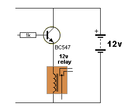
Fig 71m
Figs 71m shows a relay connected in the emitter of a
transistor. This configuration is called an emitter-follower.
When the transistor turns off, the relay is de-energised and a
back-voltage is produced.
The voltage on the top of the relay becomes less than 0v and
this pulls the emitter DOWN. This has the effect of turning ON
the transistor and for a tiny fraction of a second, the effect
of the relay is cancelled by a flow of current through the
transistor. This prevents a high back-voltage being produced and
thus a diode is not needed.
One point about emitter-follower designs:
The voltage on the relay is less than 12v due to the 0.7v
between the base and emitter and the base will be lower than 12v
by as much as 1v. Compare this with the common-emitter driver
where the collector-emitter drop will be as low as 0.4v.
Back EMF is also produced by motors and is known as "commutation
noise." This "noise" can also be suppressed via a capacitor and/or small
inductors in the leads. The size of the voltage must be measured when
the circuit is operating as it is a "spike" and this spike will puncture
a semiconductor (such as a transistor).
Back EMF is also produced by coils, called INDUCTORS. An inductor is
also called a choke.
When a piezo is placed across an inductor, and a signal is delivered to
the parallel-pair, the piezo will detect the high-voltage (Back EMF) and
produce a very load output. The inductor produces the high voltage when
the signal is turned off sharply. The magnetic flux collapses and
produces a very high reverse voltage. A typical circuit that takes
advantage of this high voltage is the:
Wailing Siren
Before
we move on to the next phase of this discussion, there is one
interesting point that needs covering.
When a circuit has a number of amplifying stages, there is always a
possibility of noise being generated in one of the transistors in the
"front-end" (the first or second stage in the amplifier) and this is
amplified by the stages that follow. This is the case with the Hearing
Aid Amplifier in Fig 69.
FILTERS
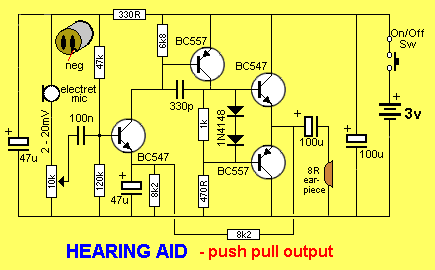
Fig 69.
The 330p between the
base and collector of the BC557 removes high-frequency noise. If
the 330p is removed a 1MHz waveform is generated in the
front-end and amplified by the stages that follow. This noise
cannot be heard but is visible on a CRO (Cathode Ray
Oscilloscope) and causes the circuit to take extra current. The
330p capacitor provides NEGATIVE FEEDBACK to remove the
waveform completely.
We have studied circuits
that use components to produce NEGATIVE FEEDBACK. The first circuit we
studied was the self-biased common-emitter stage. The base-bias resistor
provided negative feedback to set the voltage on the collector.
Any component (resistor or capacitor) connected between the output and
input of a stage produces NEGATIVE FEEDBACK.
A resistor connected between the output and input produces about the
same amount of feedback no matter what frequency is being process by the
amplifier.
But a capacitor provides more feedback as the frequency increases.
That's because the effective "resistance" of the capacitor decreases as
the frequency increases.
This feature can be used to "kill" the amplitude of high frequencies and
thus only allow low frequencies to be amplified.
It can also be used to only allow high frequencies to be
amplified. When it is used to couple two stages, a low-value capacitor
will only allow high frequencies to pass from one stage to the next.
By using a resistor in series with a capacitor, the effect of the
capacitor can be controlled.
Using these facts, we can design circuits that will amplify low
frequencies or high frequencies. This type of circuit is called a
FILTER.
A Filter can be given a number of names. Here are a few:
Active Filter contains a transistor or op-amp in the circuit
High Pass Filter suppresses or rejects the low frequencies
Only the high frequencies appear on the output
Low Pass Filter suppresses or rejects the high frequencies
Only the low frequencies appear on the output
Notch Filter: A Filter that rejects or suppresses a narrow
band of frequencies.
To understand how a filter works, you need to know "HOW A CAPACITOR
WORKS."
|
|
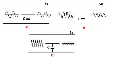
Fig 72a shows a capacitor with a low-frequency signal entering
the left terminal. The output amplitude from the capacitor in diag a will be small because the capacitor is able to charge and discharge as the signal rises and falls. As the frequency of the signal increases, the output increase in amplitude because the capacitor does not have enough time to charge and discharge and thus it does not "absorb" the amplitude of the signal. |
|
|
Fig 72b shows a capacitor connected between the "signal line" and
0v rail. When a low-frequency signal is on the "line," the capacitor has
little effect on attenuating (reducing) the amplitude, as shown in diag
a
because the capacitor charges and
discharges just like pushing a "shock absorber" up and down slowly.
As the frequency of the signal increases, it is reduced in amplitude because the signal is trying to charge and discharge the capacitor very quickly and it takes energy to do this and the energy is coming from the signal. |
|
|
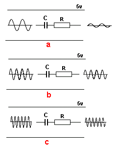
Fig 72c Fig a shows a capacitor and resistor connected in series on the
"signal line." With a low-frequency signal, the capacitor reduces
the amplitude because most of the signal is absorbed by the capacitor
charging and discharging. As the frequency increases (fig b), the output will be reduced by a smaller amount because the capacitor has less time to charge and discharge and less time to "absorb" the signal. As the frequency is increased further (fig c), the resistor starts to have an effect on reducing the amplitude because these two components are connected to other components in a circuit and a higher frequency has a higher energy and more of this energy gets lost in the resistor - thus reducing the amplitude slightly. In addition, the capacitor is already charging and discharging as quickly as possible and it is transferring as much of the signal as possible. It is only the resistor that is creating the attenuation at high frequencies. It does not matter if the capacitor or resistor is placed first or last, the attenuation is the same. |
|
|
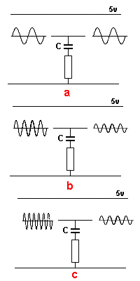
Fig 72d
Fig a shows a capacitor and resistor connected in series
between the "signal line" and 0v rail. With a low-frequency signal the
capacitor can charge and discharge and the voltage across it will rise
and fall so the effect on the amplitude of the signal is minimal. The resistor has very little effect on reducing the amplitude. The top plate of the capacitor rises and falls with the signal and the bottom plate rises and falls very little. As the frequency increases, the capacitor cannot charge and discharge fast enough and more of the energy of the signal goes into charging and discharging it. The top plate of the capacitor is rising and falling very quickly and this is making the lower plate rise and fall a small amount. This puts a small current though the resistor and this has an effect on reducing the amplitude. The amplitude of the output is reduced as shown in Fig b. As the frequency is increased further as shown in dia c, the top plate of the capacitor is rising and falling as fast as it can and the lower plate is rising and falling too. This puts most of the amplitude-loss in the resistor but the signal is not reduced any more. It does not matter if the capacitor is above or below the resistor, the attenuation is the same. |
|
Once you have a concept of the way a capacitor reacts to a high and low
frequency, you can see how a circuit will pass or prevent (attenuate) a
signal. There are many different types of filters and they are all designed to improve the output of a poor signal, such as removing background "hiss" or "rumble" in audio recordings. The following two circuits show the effect of adding capacitors and resistors between the output and input: |
|
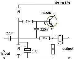
|
Fig 72e is a low-pass filter that provides unity voltage gain to all frequencies below 10KHz, but it rejects all frequencies above 10KHz at 12dB per octave. It is used to remove high frequency noise from audio recordings. |
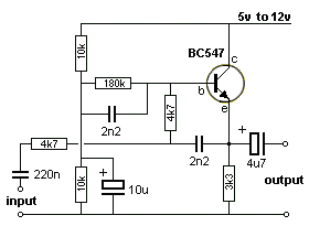
|
|
Fig 72f is a high-pass filter
that provides unity voltage gain for all frequencies greater
than 50Hz. However, it provides 12 dB per octave rejection to
all frequencies below 50Hz. It is used to remove low frequency
noise from audio recordings. The transistor is configured as an emitter-follower biased at about half the supply value by the low-impedance junction formed by the top 10k resistor and the lower 10k in parallel with the 10u electrolytic. Negative feedback applied through the filter network of the 33k and 220n and the 10k and 220n creates an active filter response. |
|
|
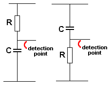
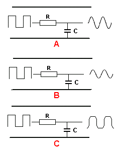
Converting a square wave to a sinewave
can be done with a
capacitor and resistor in series. The capacitor takes time to charge and discharge, (according to the value of the resistor) and the output of the circuit is where the two components join. The circuit is actually a TIME DELAY circuit, but this time we are monitoring the rise and fall of voltage on the capacitor, rather than just detecting the value after a period of time. The Square-wave to Sinewave circuit is drawn slightly different to the Time Delay circuit so you can see what is happening. The resistor is drawn at an angle of 90 degrees to the capacitor to show the signal is attenuated (reduced) in the resistor and appears across the capacitor as an amplitude. The value of the resistor and capacitor are important. When they are the correct values, the signal is a very-good sinewave with maximum amplitude as shown in diagram A. When the values are too high or too low, the result is shown in figures B and C. . |
THE "DIGITAL"
STAGE - or Digital State
also called the DIGITAL CIRCUIT or DIGITAL TRANSISTOR
| There is no such thing as a DIGITAL TRANSISTOR or
an AUDIO TRANSISTOR. All transistors are just "TRANSISTORS" and the surrounding components make the transistor operate in DIGITAL MODE or ANALOGUE MODE. It's a bit like saying money is: "food money" or "petrol money." But we have some transistors that have inbuilt resistors to make it suitable for connecting to a digital circuit without the need for a base resistor. Here is the datasheet for an NPN transistor BCR135w and PNP datasheet for BCR185w. These transistors are called "Digital Transistors" because the "base lead" can be connected directly to the output of a digital stage. This "lead" or "pin" is not really the base of the transistor but a 4k7 (or 10k) resistor connected to the base allows the transistor to be connected to the rest of a digital circuit. You cannot actually get to the base. The resistor(s) are built into the chip and the transistor is converted into a "Digital Transistor" because it will accept 5v on the "b" lead. The 47k is not really needed but it makes sure the transistor is fully turned OFF if the signal on the "b" lead is removed (in other words - if the input signal is converted to a high-impedance signal - see tri-state output from microcontrollers for a full explanation). This transistor is deigned to be placed in a circuit where the input changes from low to high and high to low and does not stop mid-way. This is called a DIGITAL SIGNAL and that is one reason why the transistor is called a digital transistor. (However you could stop half-way but the transistor may heat up and get too hot). Any transistor placed in a digital circuit can be called a "digital transistor" but it is better to say it is operating in DIGITAL MODE. |
"n" indicates any number of inputs. ("n" is an
unspecified number.) We have shown circuits with the load (such as a speaker or
LED) above the transistor or below (it cannot be in both places at the
same time). The position of the LOAD introduces two new terms:
All the circuits and stages
we have discussed have been amplifiers for audio signals.
However there is another signal that can be processed via an amplifier.
It is called a digital signal or "Computer" signal. It is a signal that
turns a transistor ON fully or OFF fully.
The simplest example of a digital circuit is a torch. The globe is
either ON or OFF. But a torch does not have any transistors. We can
simply add a transistor and the circuit becomes
DIGITAL CIRCUIT.
A
Digital Circuit
has
2 STATES: ON
and
OFF. It is never half-ON or half-OFF.
The secret to turning a transistor ON fully is base current. If you
supply enough base current the transistor will turn ON FULLY.
The Digital Circuit is the basis of all computers. It produces an
outcome of "0" when not active or "1" when active.
This is called POSITIVE LOGIC.
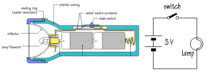
Fig 72.
Fig 72. A TORCH is
an ON-OFF circuit.
A Digital circuit is an ON-OFF circuit.
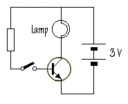
Fig 73.
Fig 73. This is the
simplest DIGITAL CIRCUIT. The globe illuminates when the switch
is closed.
Whenever a transistor is used in a stage that has a defined ON
state and OFF state, it is using the OFF and ON state of the
transistor and the transistor is called a DIGITAL TRANSISTOR.
It is simply an ordinary transistor used in a "DIGITAL WAY."
It is NOT a special type of transistor.
Two reasons why a Digital Circuit was invented:
1. It produces either "0" or "1" (LOW or HIGH) and these are
accurate values. By combining millions of "digital circuits" we can
produce counting and this is the basis of a computer.
2. When a circuit is OFF, it consumes no power. When a circuit is
fully ON the transistor also consumes the least power. This is because
the globe is illuminated brightly and the transistor
remains cool - as it has the lowest voltage across it.
The "ON" "OFF" states are called LOGIC STATES or
DIGITAL
STATES and when two transistors are put together in a circuit with "cross-coupling"
they alternately flash one globe then the other.
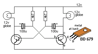
Fig 74.
Fig 74. This circuit
is called a FLIP FLOP or ASTABLE MULTIVIBRATOR.
(AY-STABLE - meaning not stable)
Using a transistor as a switch is exactly the same as using
it in DIGITAL MODE or in a DIGITAL CIRCUIT or in a
LATCH CIRCUIT or any other circuit where the transistor changes from
OFF state to ON state VERY QUICKLY.
A transistor in this type of circuit is called a SWITCHING TRANSISTOR
and it may be an ordinary audio transistor but it is called a switching
transistor when used in a switching circuit.
The two Darlington transistors in Fig 74 are SWITCHING
TRANSISTORS and the circuit is an
ASTABLE MULTIVIBRATOR.
One of the most common circuits is used to activate a relay. A relay
must be turned ON or OFF. It cannot be half-on or half-off. The
transistor changes from OFF to ON very quickly. It is called a switching
transistor.
All transistors used in a DIGITAL CIRCUIT are switching
transistors. DIGITAL CIRCUITS or DIGITAL LINES are either
HIGH or LOW.
When a digital transistor is turned ON (saturated) the output is
LOW. When a digital transistor is OFF the output is HIGH.
The output is taken from the collector of a common-emitter stage.
This is called two MODES of operation. ON and OFF.
Any circuit that operates in TWO MODES is called a DIGITAL
CIRCUIT.
Any circuit that drives (powers) a relay is essentially a
DIGITAL CIRCUIT. Sometimes the driving circuit can gradually turn ON and
when the collector current is sufficient, the relay pulls-in.
When the collector current falls to a lower value, the relay
drops-out.
We like to think of the driver stage as a digital stage so that we
guarantee the relay will pull-in and drop-out.
Here's an important feature that has never been mentioned before:
A relay must pull in quickly and firmly so the contacts close with
as much pressure as possible. This prevents arcing when closing and
opening and ensures a long life for the relay.
That's why the driver circuit should be an ON-OFF or DIGITAL design.
The following circuits are NOT high-speed, but will activate a relay
successfully.
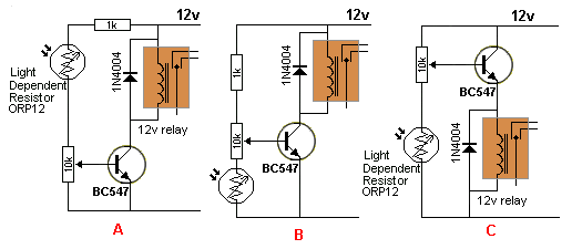
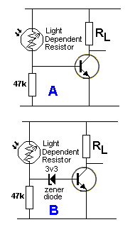
Circuit A activates
the relay when light falls on the LDR. The level of illumination can be
adjusted by the 10k pot.
Circuit
B activates
the relay when the illumination reduces. The level can be adjusted by
the 10k pot.
Circuit
C
is an emitter
follower and although it works in a similar way to circuit B, the
voltage on the collector is less than 12v by about 1v and this creates
extra loss and added temperature-rise in the transistor.
A 12v relay might work on a 9v circuit, but as we said
above, the relay needs to close with as much pressure as possible to
prevent the contacts arcing.
A 6v relay will work on a 12v circuit if you add a 5v1 or 5v6 zener in
series with the coil.
A 12v relay will work on a 24v circuit if you add a 12v zener.
If the driver transistor turns on and OFF very fast, you will
need a diode across the coil to prevent the back voltage damaging the
transistor when the relay turns OFF.
The circuits above operate very slowly and a diode is not needed.
THE UNIJUNCTION TRANSISTOR
etc
DRIVING A
RELAY via CONSTANT CURRENT
A relay can be driven by a circuit called a CONSTANT CURRENT
CIRCUIT and this means the maximum current delivered to the
relay is fixed by the driving transistor. This means the supply
voltage can rise higher than the recommended voltage and the
relay will still be supplied with its rated coil current.
The circuit can also be called CURRENT LIMITING or
CURRENT CONTROLLING or MAXIMUM CURRENT.
For this circuit to work you must know the current required by
the coil for it to pull-in effectively.
This value can be obtained from the specification sheet for the
relay. It will specify the coil voltage and the coil resistance.
In our example the coil is 12v and the resistance is 360 ohms.
This identifies the relay as requiring 33mA to close the
contacts.
Most relays will work on a slightly lower voltage and slightly
higher voltage, but if the supply ranges from 12v to 24v, you
need this type of circuit:
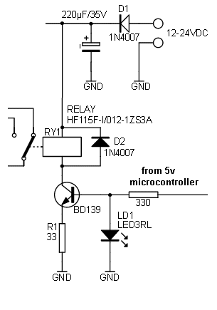
The BD 139 only
allows (a maximum of) 33mA to flow because the base sees 1.7v due to the
characteristic of the red LED.
The voltage between base and emitter is 0.7v and this
means 1v will be dropped across the 33R when the current rises
to 33mA.
Suppose you fit a relay requiring 100mA. If it is a 12v relay,
it will have about 120R coil.
The transistor will turn ON and the current will increase. As
soon as the current reaches 33mA, the voltage across the 33R
will be 1v and since the transistor is only seeing 1.7v on the
base, if the current rises any further, the voltage across the
33R will rise and the voltage between base
and emitter will be less than 0.7v. This will cause the transistor
to turn
OFF slightly.
This means only 33mA will flow through the relay and it will not
be enough to close the contacts.
The relay will not work.
If you increase the supply from 12v to 24v, the current will not
rise above 33mA and the relay will still not work.
If you fit the 33mA relay and increase the voltage from 12v to
24v, only 33mA will flow though the relay and 12v will appear
across it. The other 11v will appear across the
collector-emitter terminals of the transistor and 1v will be
across the 33R.
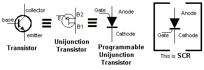
The Unijunction Transistor (UJT) and
the Programmable Unijunction Transistor (PUT) and the ordinary
transistor ARE ALL THE SAME.
A voltage on the base or the "E" lead or the Gate, will turn them
all on and the resistance between all the
leads will reduce to a small value.
Actually a small voltage will develop between the leads and this is
called a characteristic voltage and cannot be altered.
BUT here are the differences. The voltage on the base of the
ordinary transistor is about 0.7v to turn it ON. The voltage on the
Unijunction Transistor can be up to 3.5v The voltage on the Gate for
the PUT is about 0.7v and can be slightly higher or lower.
When the voltage is removed from the base, "E", or Gate, the device
"turns OFF."
If you add a voltage divider to the base of the ordinary transistor,
you can turn it on at say 1v or 2.6v or any value. You can call this
"programming the transistor"
That's what a Programmable Unijunction Transistor is. It is an
ordinary Unijunction Transistor that can be placed in a circuit with
voltage divider resistors so the device turns on at a particular
voltage.
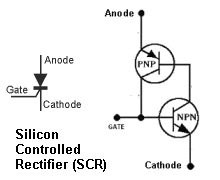
A
Silicon Controlled Rectifier has a different feature. When the
voltage on the Gate turns the SCR ON, it "latches" and stays ON
until the supply voltage is removed and the current through the SCR
falls to zero.
The two diagrams opposite are NOT identical. The SCR remains "latched" via
the Gate. Making the Gate 0v, will not unlatch the SCR.
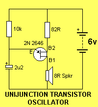
The UJT circuit shows a typical
arrangement with a low-impedance device, such as a speaker,
between B1 and 0v rail.
The way it works is this:
The capacitor charges via the 10k resistor. During this time the
resistance between B1 and B2 is infinite. The charging is a sawtooth
waveform because the charging is a rising gradient and the discharge
is very rapid - into the speaker. The emitter detects when the
voltage rises to about 3.5v to 4v (this is a characteristic of the
UJT device) and at this point the
transistor "turns on" and the resistance between the Emitter and B1
becomes very low and is effectively equivalent to a diode in
forward-bias.
The voltage (the energy) in the capacitor is then passed to the
speaker and this produces a "click." This is the only way the
speaker gets its energy. The voltage across the capacitor falls very
rapidly and when it reaches less than 0.7v, the
transistor turns off and the cycle repeats.
LATCH CIRCUIT -
an SCR made with transistors
Why can't you use an ordinary transistor in
the circuit above?
Because an ordinary transistor turns ON slowly when the voltage
is 0.55v and turned on more at 0.6v and turned ON fully at
about 0.7v. There is only a very small "gap" between 0.55v
and 0.7v and this would be the charging and discharging voltage
for the electro. But during this range the transistor is turning
ON too and effectively removing the charging capability of
the 10k to charge the electro and thus the circuit would never work.
You can't use an SCR because it "latches" and the cycle will not
repeat.
One of the
main differences between Unijunction and PUT:
A Unijunction Transistor needs about 2v to
3.5v to turn ON.
A Programmable Unijunction Transistor turns on at 0.2v to 1.6v
(normally 0.5v to 0.7v)
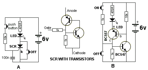
Fig 75. Latch Circuit
Fig 75. Circuit B
is a LATCH. The two transistors instantly change from the OFF
state to the ON state.
This is also classified as a DIGITAL CIRCUIT. The circuit can
also be called an SCR made with transistors. Circuit A shows an
SCR in action. The top switch turns the SCR ON and it stays ON
when the button is released. To turn the SCR off, the lower
switch is pressed.
The SCR in circuit A produces a
'LATCH.'
The SCR can be replaced with two transistors as shown in circuit
B.
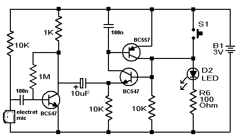
Fig 75aa. Latch Circuit
Fig75aa is a LATCH and the PNP/NPN
transistors are "latched-on" by pressing S1. The circuit will
also turn on with a resistor as high as 15k across S1 as we only
need to put 0.6v on the base of the BC547 transistor. The 10k on
the base forms a voltage divider and this determines the
resistance of the "turn-on" resistor. The emitter of the BC547
transistor does not move when this voltage is applied and the
collector of the BC547 pulls the base of the BC557 down to turn
the PNP transistor ON. This action takes over from the 15k
resistor and the two transistor remain ON.
The base of the BC547 is pulled to nearly rail voltage and the
emitter is 0.6v lower. The 10u electrolytic charges to cater for
the voltage-difference between the collector of the first
transistor and the voltage on the emitter of the BC547.
When the first transistor turns on, the voltage on the collector
reduces and this pulls the positive lead of the 10u towards the
0v rail.
The negative lead of the 10u cannot fall as it is connected to
the emitter of the BC547.
This means the 10u discharges and when the first transistor
turns off, the positive lead rises and takes the negative lead
with it. This reduces the voltage on the emitter of the BC547
and the transistor turns OFF.
This is how the LED turns off.
Further blowing into the microphone will make the emitter lead
of the BC547 rise and fall and this will make the LED flicker,
just like trying to blow out a candle.
Fig 75a. Latch Circuit
Fig 75a. This circuit
is a LATCH. The two transistors instantly change from the OFF
state to the ON state when the input voltage rises above 0.6v
The 22k POSITIVE FEEDBACK resistor keeps the circuit
ON when the input voltage is removed.
The 6v supply must be removed to turn the LED off.
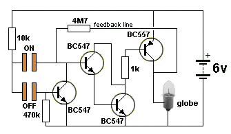
Fig 76. Touch Switch
Fig 76. This is a
circuit of a TOUCH SWITCH. Touching the "ON" pads turns
ON the
second and third transistors as they are a SUPER-ALPHA PAIR or
DARLINGTON arrangement and have a very high input impedance and
very high gain. The output of this pair goes to a PNP transistor
that amplifies the 5mA current from the Darlington to deliver
250mA to the globe.
A feedback line from output to input via a 4M7 keeps the circuit
ON when your finger is removed and provides a "Keep-ON" voltage
(and current).
The first transistor removes this
"Keep-ON" voltage and current
when a finger is placed on the OFF pads. .
How can you tell a
DIGITAL CIRCUIT
from an
ANALOGUE CIRCUIT?
1. Absence of capacitors.
There are
NO
capacitors in a
DIGITAL CIRCUIT.
2.
A switch or push-button will be activating the circuit.
3.
The circuit will be driving a
DIGITAL
or
ON - OFF
item such as a relay or globe.
The two states of a transistor in a DIGITAL CIRCUIT are: OFF -
called "CUT-OFF" and ON - called "'SATURATION."
To saturate a transistor the base current is simply increased until the
transistor cannot turn on any more. In this state the collector-emitter
voltage is very small and the transistor can pass the highest current
and the losses (in the transistor) are the lowest.
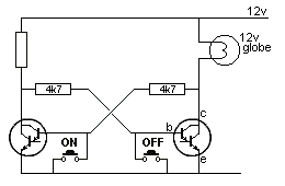
Fig 77.
Fig 77. This circuit
has only two states. ON and OFF. The ON button turns off the
first transistor so the second transistor turns the
globe ON.
This is called a TOGGLE ACTION and the circuit is a BINARY
CIRCUIT or BISTABLE CIRCUIT called a BISTABLE SWITCH or a bistable
of the MULTIVIBRATOR family (BISTABLE MULTIVIBRATOR).
It can also be called a LATCH as it stores one bit of
information and is the basis of a COMPUTER.
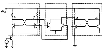
Fig 77b.
Fig 77b. This is
part of a counting circuit and since it takes many
transistors to create a circuit to count to "2" it is not
practical to make it using discrete components. That's why
INTEGRATED CIRCUITS were invented where dozens, then hundreds
then thousands then millions of transistors are connected to
produce counting chips and "bit-storing chips" and
many
other requirements.
Before we cover our next type of circuit, we will explain a 2-transistor
directly-coupled arrangement from Figs 52 and 66. It is interesting as
it can be used as a digital circuit or an analogue circuit.
THE SCHMITT TRIGGER
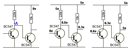
Fig 78.
Fig 78. Two facts to
note:
1. Point "A" never rises above 0.6v as it is connected to the base of
the second transistor.
2. When the first transistor is turned ON, the collector-emitter
voltage is 0.3v and the second transistor is OFF - this is
because the base of the second transistor needs 0.6v to turn ON.
In other words, when one transistor is ON the other is OFF.
There is a very brief change-over point where the first
transistor turns ON a little more and the second transistor turns
OFF a very large amount. If you can find and maintain this change-over point, the two
transistors will work in analogue mode with high gain but if you
pass this point very quickly, the two transistors will
operate as a switch in DIGITAL MODE.
We can turn this circuit into a DIGITAL CIRCUIT.
The secret to doing this is FEEDBACK and the name of the circuit is a SCHMITT
TRIGGER:.
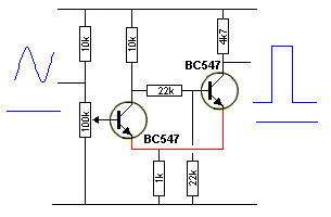
Fig 79a. Schmitt Trigger Circuit
Fig 79aaa. Basic Schmitt Trigger
Fig 79a. A Schmitt
Trigger takes a slowly rising or falling voltage and turns it
into a fast-acting ON-OFF signal. The secret is the feedback
line shown in red.
The circuit can also be called a
"sinewave-to-square-wave generator."
When the input is LOW the output is LOW.
It is a form of bi-stable multivibrator.
The distance between the lower voltage and the upper voltage (at
which the circuit changes state) is called the HYSTERESIS GAP. This
can be widened or narrowed via the 1k resistor (the 100k pot
needs to be re-adjusted when the 1k is changed).
Fig 79aaa.
The basic Schmitt Trigger only needs 3 resistors. This is
shown in
Fig 79aaa.
When the first transistor is conducting (turned ON) and the
second transistor is OFF, a voltage develops across the 1k due
to the collector-emitter current of the first transistor.
When the first transistor turns OFF, about the same current
flows though the 10k collector-load, through the base of the
second transistor, plus current flows through the 4k7 load
resistor. This means about three times more current flows
through the 1k emitter resistor and thus the voltage across it
will increase about 3 times. This is the
HYSTERESIS
voltage of the
circuit.
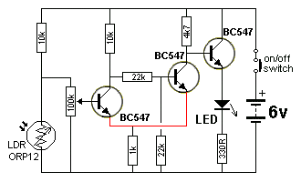
Fig 79. Schmitt Trigger Circuit
Fig 79. This circuit takes a slowly rising or falling voltage and turns it
into a fast-acting ON-OFF signal to operate a LED or relay.
This is done via the positive feedback line shown in red. It is
called positive feedback because it ADDS to the change to speed
it up.
This circuit is fully explained in the:
Talking Electronics website CD.
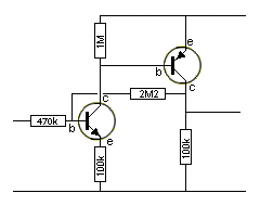
Fig 79aa. A Schmitt Trigger
Fig 79aa is a Schmitt
Trigger made from NPN and PNP transistors.
As the voltage on the input rises, the first transistor is
turned on slightly and a small voltage is developed across the
100k emitter resistor that reduces the "turn-on" effect
slightly. This means the input voltage must rise more. As the
input voltage rises more, the second transistor starts to turn
on and the collector voltage rises. This voltage is passed to
the base of the first transistor to assist the input voltage and
because the collector voltage of the output transistor rises
considerably, it has a large effect on turning ON the first
transistor. They turn each other ON until they are both fully
turned ON.
The 2M2 has taken over from the 470k and made the base of the
input transistor slightly higher. The input voltage has to drop
a small amount before the pair will start to turn off.
The circuit has created a small gap between the low and high
input voltage (and between the HIGH and LOW input voltages)
where the circuit does not change from one state to the other.
This gap is called the HYSTERESIS GAP.
The output of the Schmitt Trigger in Fig 79aa is classified as
"high impedance" (due to the value of the 100k on the output)
and this must be connected to a stage with a high input
impedance so the voltage on the output of the Schmitt
Trigger is not affected.
Here is another Schmitt Trigger:
 The
only problem with this circuit is the load is not pulled very
close to the 0v rail. The minimum voltage across the PNP
transistor is about 1.5v, however the circuit works well and
provides a wide voltage between ON and OFF. It has been
tested with a load of about 30mA across the 100R.
The
only problem with this circuit is the load is not pulled very
close to the 0v rail. The minimum voltage across the PNP
transistor is about 1.5v, however the circuit works well and
provides a wide voltage between ON and OFF. It has been
tested with a load of about 30mA across the 100R.
Changing the 470R to 1k increases the "gap."
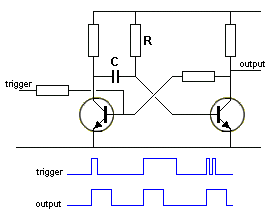
Fig 79ab. The Monostable or
"Pulse Extender."
Fig 79ab.
Before we leave the MULTIVIBRATOR family, the third type of
Multivibrator is the MONOSTABLE MULTIVIBRATOR.
It is only stable in ONE state. This is called the "rest" state.
The other state is "timed" via a capacitor.
The circuit is triggered and it changes to the other stage and a
TIMING CAPACITOR C charges via a resistor R (called a TIMING
CIRCUIT) and a multiplication of the two produces a value called
the
time constant.
When it is charged, the circuit drops back to the
rest state.
While the output is high, input pulses (trigger pulses) have no effect on the
circuit. Also, if the input is triggered and kept high longer
than the time constant of C and R, the output will NOT stay
high for longer than the time constant.
This circuit is also called a PULSE EXTENDER.
GATES
We have described the transistor as an amplifier and the fact that
POSITIVE FEEDBACK can turn a transistor ON more and more,
so it changes from: "not-turned-ON" to
"fully-turned-ON"
in a very short period of time. When a transistor is operating
in this mode, it is said to be in DIGITAL MODE. We saw the
effects of DIGITAL MODE in Figs 74, 75, 76, 77 and 78. The
advantage of digital mode is the transistor dissipates the least
heat in either state.
The transistor can be put into a chip (IC - Integrated Circuit) and used
in Digital Mode. When this is done, the transistor is put into a circuit
called a GATE. A Gate is simply a BUILDING BLOCK in which
the output changes from LOW to HIGH or HIGH to
LOW very quickly. The simplest GATES are called AND, OR,
NAND, NOR and NOT. In general a GATE operates on a 5v supply (this
applies to gates in the TTL family. They cannot withstand a voltage
higher than 5.5v. CMOS gates operate to about 14v-16v and some are
up to 20v) and the
input has to change from LOW to HIGH or HIGH to
LOW very quickly and the output will change from LOW to
HIGH or HIGH to LOW very quickly. You may think the
gate is not achieving anything, but most gates have 2 or more inputs and
the output is "more powerful" than the input. The introduction of
GATES revolutionised the development of the computer and was the
beginning of the DIGITAL AGE.
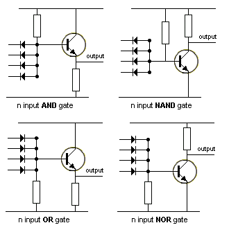
Fig 79ac.
Fig 79ac
shows AND, OR, NAND, NOR and NOT gates produced with
transistors.
SINKING AND SOURCING
|
|
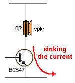
Fig 79b. When the
speaker (LOAD) is placed above the transistor, the circuit is said to
be SINKING the current. A BC547 does not have the
collector-current to adequately supply an 8R speaker. You really
need a BC338. |
|
|
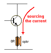
Fig 79c. When the
speaker (LOAD) is below the transistor, the circuit is said to
be SOURCING the current. The only difference between the two circuits is the voltage on the base. Fig 79b will operate with a base-voltage less than 1v, while Fig 79c is an emitter-follower design and will need a voltage on the base from about 1v to full rail voltage. |
|
|
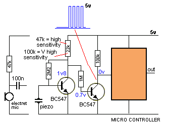
Fig 79d. In this
circuit the first transistor is self-biased and the 2M2 base
bias resistor turns the transistor ON and the voltage on the
collector is only about 1.8v. This means the collector has to drop by only 1.2v for the second transistor to turn off and the 100k will produce 5v on the input to the microcontroller. If the transistor has a gain of 100, the electret mic or piezo has to produce a 12mV signal to activate the circuit. When the load resistor is increased to 100k, the collector has about 850mV on it, and it only has to drop 300mV for the signal to enter the microcontroller. This makes the 100k load resistor produce a more-sensitive circuit. When no audio is being detected, the output of the second stage is 0v. |
|
|
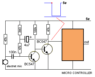
Fig 79e. This circuit has been taken from Fig 71acc. It is a bootstrap circuit and produces a very clever "switch." The circuit sits with the first transistor turned ON and the second turned OFF as can be seen in the first line at the top of the output waveform - up to the red dot. When a signal is picked up by the microphone (this is the red dot on the waveform), a negative-going signal of about 100mV will turn the transistor off slightly and the second transistor will turn ON. The 4u7 will be "pulled down" and completely take over from the signal from the microphone. It will turn the first transistor off more and the second transistor will be turned ON more. This will continue until both have completely changed states. |
|
They will stay like this until the 4u7 is charged in the
opposite direction and the base of the first transistor sees
0.7v. This causes the second transistor to turn off and the 4u7
rises and turns the first transistor ON more. The 4u7 gets
slowly discharged and the circuit remains in this state. The circuit produces a very clean output every time it detects audio. The duration of the low in the graph can be shortened by reducing the value of the electrolytic. |
|
|
|
Fig 79f interfaces a phase-shift
oscillator (see Fig 90) to a speaker. This is a very
difficult thing to do as the phase-shift oscillator has an output
that is very close to rail-to-rail and any loading of the output
will cause it to stop working. In an attempt to interface the oscillator to a speaker we have added an emitter follower transistor and a 1k separating resistor, plus a 100R in series with the speaker. This should give a loading of about 20k and the circuit should work. Otherwise the 10k will have to be reduced or the 100R increased. |
ANALOG TO DIGITAL
The second
transistor in Fig 80e is called
a DIGITAL STAGE. This simply
means a biasing resistor is not connected to the base of the second transistor
so it turns on fully when a signal greater than 650mV is
detected and is turned off at other times. This stage is ideal for
a micro or other Digital Stage as only two voltage levels are delivered. Either 0v or rail
voltage (5v).The other advantage is it does not take any
quiescent (idle) current.
5v to 3v3: See also LEVEL CONVERSION using an Inverter
Many
of the circuits we have described convert an ANALOG signal to a DIGITAL
signal.
These are called ANALOG TO DIGITAL CONVERTERS but we have not
given them this specific name because we have been concentrating
on other features.
We will now cover the concept of Analogue to Digital Conversion.
An ANALOGUE signal
rises and falls but doesn't have any defined amplitude or frequency.
This signal cannot be delivered reliably to a circuit that requires a DIGITAL
SIGNAL as the amplitude may not be large enough.
A DIGITAL CIRCUIT requires a digital signal and this type of
signal is either a constant HIGH or LOW and the amplitude must be very
close to rail voltage or almost 0v. And it must change from one state to
the other very quickly.
Delivering a high amplitude analogue signal may be recognised by
a digital circuit when it reaches a peak or goes to 0v, but this is not
guaranteed or reliable.
In addition we may want the signal to be a CONSTANT HIGH when the audio
is present.
This is what an ANALOG TO DIGITAL circuit will do. It will
produce a constant HIGH when audio is present and ZERO (LOW) when the
audio is not present. Or pulses that are nearly rail voltage and very
close the 0v.
Recapping:
To convert an analogue signal to a digital signal we need to deliver
ZERO OUTPUT (called a LOW output) when the signal has a small amplitude and a
HIGH output when the signal has a high amplitude.
To do this we use a common-emitter stage, as it has a high voltage-gain
and this is what we need.
There are many ways to convert an Analogue signal to a Digital signal
but the basic way is to amplify the signal by a large
amplification-factor so the resulting waveform will rise to the voltage
of the rail (or even higher). It cannot go higher than rail
voltage but you will see what we mean in a moment.
This is normally called "over-driving" the signal and if this is done in
an audio circuit, the result is distortion. But we are not going to
listen to the output, so we take advantage of this feature to produce a DIGITAL OUTPUT.
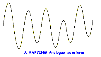
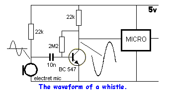
Fig 80a
Fig 80a shows an analogue signal. It is made up of lots
of sine-waves and may be as high as 2v or only a few millivolts.
Low-level signals
are generally expressed in mV, to make them instantly
recognisable and easy to talk about.
In general this type of signal will be too small to be detected by a
Digital Circuit. A Digital Circuit needs a signal greater than about 3,500mV so
the waveform appears on the input line as a HIGH, during the peak
of its excursion. It should be nearly 5,000mV for
reliable detection.
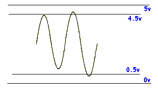
Fig
80b. A Digital
Circuit will detect a waveform larger than 4.5v as a HIGH and
less than 0.5v as a LOW
Fig 80b.
Only the large excursion(s)
will be detected by a Digital circuit as the other parts
will not rise high enough to be detected. To increase the analogue signal to as
much as 5,000mV, an amplifier is needed.
Fig
80c.
The amplifier maybe one
or two stages, depending on the amplitude of the original signal.
Each stage of an amplifier will increase the size of the signal about 70
times. If you are very lucky, you may get an amplification of 100x (100
times). Thus a 5mV signal with one stage of amplification will produce a 350mV
to 500mV signal. This is not sufficient to be detected by
a Digital Stage. Another stage will easily produce a full 5,000mV signal.
The second stage only needs to amplify the signal about 10 to 12
times and a higher gain simply
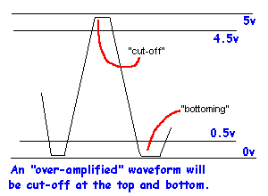
drives the waveform into "bottoming"
and "cut-off" as shown in fig 80c.
Fig
80d.This means the waveform
will be "clipped" at the top and bottom and converted to a fairly
"square-ish" shape.
Suppose you have a waveform that is higher than 5mV (say 30 - 50mV) and
want to know if it will trigger a Digital Circuit with a single stage of
amplification.
Connect the components as shown in Fig 80d and write a program to illuminate a LED when the waveform is detected.
There is only one problem
with the circuit in Fig 80d.
At the end
of a whistle or speech, the LED may be illuminated or
extinguished. It all depends on the last cycle of the
waveform. The circuit sits with the output approx mid-rail
and the micro does not know if this is a high or low, and
takes the reading by the direction of the last cycle.
Some of the inputs of a micro are Schmitt Triggered. This means a HIGH
has to be 85% to 100% of rail voltage for it to be seen as a HIGH and
between 20% and 0% to be seen as a LOW.
The non-Schmitt Trigger inputs see a LOW as 20% to 0% and a HIGH
as above 2v for 5v operation.
If the last cycle went from zero to mid-rail the micro will
see the waveform as a low on Schmitt Trigger inputs and a
HIGH on the other inputs. This problem can be overcome by
adding a second stage that only produces a LOW when audio is
detected. It also increases the amplitude of the audio to
guarantee triggering of the Digital Circuit. This is shown
in Fig 80e.
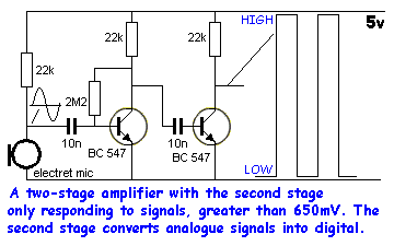
Fig 80e.
This stage is only suitable if you are sure you have plenty of
"over-voltage" to drive the transistor into saturation. By this we mean
you must have at least 1v (1,000mV) drive signal so you can be sure the
transistor will turn on (saturate).
The fast rise and fall times means you have a "clean" HIGH and LOW.
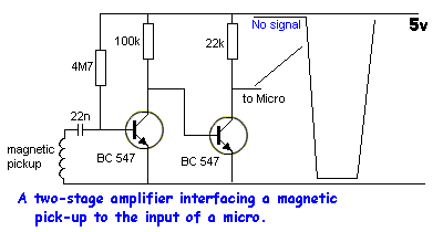
Fig 80f.
Fig 80f couples a magnetic pick-up to the amplifying circuit
so the biasing of the first transistor can be determined
by the value of the base-bias resistor. The coil cannot be
connected directly to the transistor as the low impedance
(resistance) of the coil will upset the bias on the base.
With
this arrangement, the descending part of the input waveform of a
few millivolts will turn off the transistor, while the ascending
part of the waveform will not have any effect.
A coil of wire of any size will be suitable and to make it an
effective collector of magnetic flux, it should have a magnetic
core such as ferrite. No other impedance-matching is necessary.
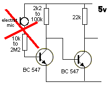
Fig 80g.
Fig 80g
shows an electret microphone connected directly to the base of a
two-transistor amplifier. This arrangement will work and
provides the best transfer of signal from the microphone to the
base.
But biasing the first transistor is a very difficult thing to
do. The electret microphone needs a very small current to
operate and the series resistor allows this current to flow.
You will need to build the circuit, select values for the base
and collector then whistle into the microphone to see which
combination produces the highest gain.
If the resistor is a small value, the base current will be high
and the transistor will be turned on fairly hard. This is called
BOTTOMING and the collector voltage will be very low.
The electret microphone will produce a signal and this will
increase and decrease the current into the base. But the reduced
current will no turn the transistor off any appreciable amount
and the signal will not appear on the collector. If the base
resistor is very high, the electret microphone will not produce
a very large output signal and again, the waveform on the
collector will be very small.
There is no way anyone can predict the best values to use. It
depends on the type of microphone, the gain of the transistor
and the rail voltage. This is a very messy design and should be
avoided. It has been included because it has been seen in
circuits on the web.
LEVEL CONVERSION or LEVEL SHIFTING
LEVEL CONVERSION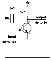
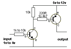
3v3 to 5vSuppose the output of a
device is 3v and you want to activate a device that requires 5v or
12v.
This circuit converts the signal that rises from about 0v to about
4v to a signal that rises from 0v to 5v or 12v.
Note: The output is not inverted, it is in-phase with the
input due to two inversions within the circuit.
The resistor values and the type if transistor will depend on the
output current required.
3v3 to 5v:
When we talk about LEVEL CONVERSION we are only interested in
TWO STATES. The zero state or LOW LEVEL and 3v3 (or 5v) or
HIGH STATE (high level).
This circuit produces and output of 0v when the input is 0v and 5v
output when the input is 3v3.
The circuit is not linear throughout the whole transition but that
is not important for a DIGITAL to DIGITAL transfer. It is only the
HIGH or LOW condition that is important.
LEVEL CONVERSION with
Diodes
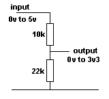
LEVEL CONVERSION with
Resistors
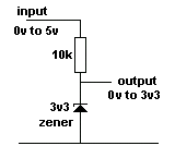
LEVEL CONVERSION with
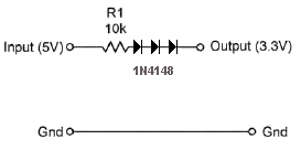
a Zener3v3 to 5v with diodes:
Level conversion can be
done with 3 diodes to change 3.3v to about 5v, but you have to know
the current-capability of the 3.3v source and the current
requirement of the 5v section.
This arrangement is only suitable for very small current
requirements.
The output is allowed to be taken HIGH by the input providing 3.3v
and the 3 diodes providing 2.1v. This allows the 4k7 to pull HIGH
with a very small current-capability.
The 10k resistor is only a safety resistor and can be removed when
the two sections are working correctly.
When the 5v line is 0v, the output is 0v. When the 5v line is 5v,
the output is about 3.2v.
5v to 3v3:
A 5v signal
can be converted to 3v3 with two resistors called a VOLTAGE
DIVIDER.
This circuit will work with both analogue and digital signals.
A 5v signal
can be converted to 3v3 with a 3v3 zener.
|
There are over 20 different types of oscillators and many more variations.
We cannot cover them all
- so we will
concentrate on the most often-used and explain how they
work. Oscillators consist of one or two transistors. They start-up by one or more components in the circuit producing "noise" or a spike from the "mains" when the circuit is turned on. Some oscillators will not start-up if the supply is increased gradually. When a spike or noise is detected, the rest of the circuit amplifies it. In most cases the noise comes from the circuit being turned ON but it can also come from the noise generated within the junction of a transistor. This noise is random and of little use, but it is fed to components such as coils and capacitors as they have the ability to produce a waveform that rises and falls smoothly and this is amplified to produce the output. When coils, crystals, capacitors and resistor are combined with transistors, many different effects and waveforms can be created and this all comes under the heading of OSCILLATORS. And the circuits are all amplifiers. An amplifier can be turned into an oscillator by providing POSITIVE FEEDBACK. The purpose of providing NEGATIVE FEEDBACK is to prevent oscillation. The purpose of providing POSITIVE FEEDBACK is to create oscillation. Positive feedback is when you take a point that is rising a large amount and pass it to a point that is also rising at the same time but only a small amount. In other words, the feedback line must be able to help or assist the small-signal line. If it does not assist the small-signal line, NO oscillation will occur. Some oscillators have a name - either after their inventor, by the way they are configured or by the shape of the wave. Some have 5 names. Some have no particular name and are just called Feedback Oscillators (positive feedback). |
|
|
Fig 80. The 10n
capacitor provides the positive feedback to keep the circuit
oscillating. |
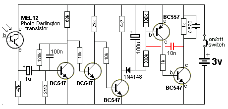
|
|
Fig 81. The 10n
capacitor provides the positive feedback to keep the circuit
oscillating. |
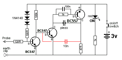
|
|
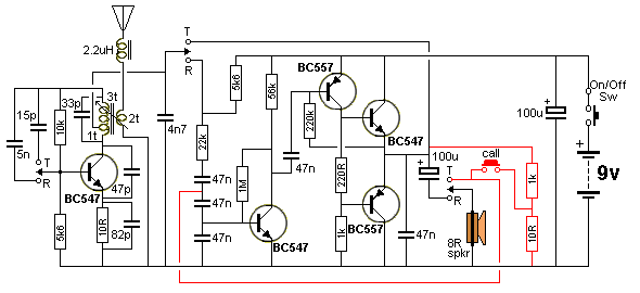
|
|
Fig 83. When the
third transistor is turning OFF, the collector voltage is rising
and this is passed to the base of the first transistor, to turn
it ON. This is how the circuit keeps "cycling" or oscillating. |
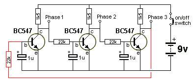
|
|
Fig 83a. The
high-gain amplifier we studied in Fig 66, for example, has negative feedback
to prevent oscillation. By using positive feedback we can turn the high-gain amplifier into an oscillator. This circuit is simply a high-gain amplifier with both transistors turning ON via the 1k and 100k resistors. This makes the voltage on the collector of the BC557 rise and the 22u and 4k7 passes this rise to the base of the BC547 to turn both transistors ON more and more until they are fully turned ON. The 22u charges a little more and this reduces the current into the base of the BC547 to turn it off a little. This effect is passed to the collector of the BC557 and the two transistors start to turn OFF. When they are fully turned off, the cycle repeats by the transistors being turned on via the 1k and 100k. |
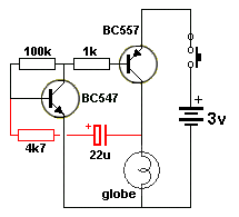
|
|
The 2-transistor amplifier we studied in Fig 42 can be changed
slightly to drive a speaker. The two common-emitter transistors
turn on together and the 22u is "lifted" to turn on the NPN
transistor harder. Both transistors turn on until fully saturated and this puts current though the speaker. The 22u charges a little more and this reduces the current into the base of the NPN transistors, turning it off a slight amount. The PNP is turned off a small amount and they both keep turning off until fully turned off. The 10k and 50k start to charge the 22u to repeat the cycle. The 22u produces positive feedback. It can be replaced by values from 100n to 22u to change the frequency of the tone. |
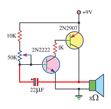
| The two circuits above are examples of LOW
IMPEDANCE outputs. If the load (the globe or speaker) is
increased above about 47 ohms, the circuit will not work. They
simply "lock-ON." This is because the capacitor (electrolytic)
must be pulled down by the load at a very critical point in the
cycle. In addition, the 100k "turn-on" (or 50k and pot) resistor
must be a very high value. If it is too low, the circuits will
"lock-ON." The critical point is this: When the circuit is fully turned-ON, the right side of the capacitor is near rail voltage and it is being charged via the bas-emitter junction of the first transistor. As it becomes fully charged, the current into the base of the first transistor reduces slightly and the transistor turns off slightly. This effect is passed to the second transistor and it turns off slightly too. The right lead of the capacitor drops and this lowers the left lead to turn off the first transistor slightly more. This is the beginning of the "turn-off section" of the cycle. If the second transistor did not have a very heavy load (low resistance load), the slight turning-off of the two transistors would not lower the capacitor and they would both remain ON. |
You can see the importance of FEEDBACK in a circuit. Some circuits will not work without feedback and some will distort. Sometimes the feedback is POSITIVE and sometimes NEGATIVE. The trick to understanding a circuit is to locate the feedback (component or "line") and work out what it is doing.
|
|
Fig 83b. Here's an
oscillator circuit. We know it must have feedback to
operate, but where is the feedback? In this circuit the 4 electrolytics are equivalent to miniature rechargeable batteries. When the circuit is turned on, they all get charged to a voltage according to the surrounding components but the 22u is the important component. The base of the BC557 sits at 4v and the emitter must rise to 4.6v for the PNP transistor to turn on. When it does, it turns on the BC547 and this transistor puts a load of 220R across the circuit. This reduces the voltage across the 470k/1M voltage divider and the base if the BC557 sees a lower voltage. During this time the 22u is acting as a miniature supply and maintaining the voltage of 4.6v on the emitter. The BC547 turns ON more and more and even though the voltage on the 22u drops, the circuit turns ON and this takes more current from the 6v battery and produces a click in the speaker. |
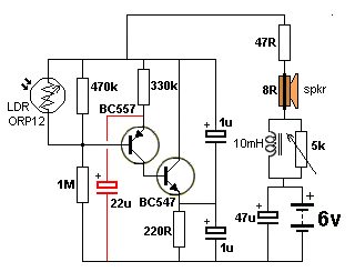
THE SQUARE-WAVE OSCILLATOR
|
|
When two
transistors are cross-coupled as shown in Fig 84, you can
safely assume the circuit will oscillate. The frequency of
oscillation will depend on the value of the components but the oscillator is
known as a FREE-RUNNING OSCILLATOR or ASTABLE (ay-stable)
MULTIVIBRATOR and the
output is a square wave. It will have an equal-mark-space ratio
if the components are the same value. This circuit is also called a FLIP-FLOP. |
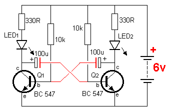
|
|
Fig 85. By
rearranging the components in Fig 84, we can draw the circuit as
one common-emitter stage driving another common-emitter stage
with a 100u providing positive feedback. The circuit relies on the power being turned on quickly for it to start up. Both transistors will turn ON but one will turn on faster than the other and prevent the other turning on. The 100u connected to the turned-on transistor will start to charge in the opposite direction and the second transistor will start to turn ON. This will pull the 100u lower and the first transistor will start to turn OFF. This will continue until both transistors have changed states. |
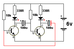
|
|
Fig 86. Here is the ASTABLE MULTIVIBRATOR with the LEDs in the emitters instead of collectors (as is normal). The frequency of oscillation is approximately 1 second. The 330 ohm resistors set the LED current to 12mA for a 6v supply. |
|
|
Fig 86a.
The LEDs can also be connected as shown in this circuit. However
the circuit takes more current than the previous designs. In the
previous designs, one side of the circuit is taking current and
illuminating the LED while the other side is turned OFF
("cut-off"). In Fig 86a, the "off" transistor is illuminating a LED while the "on" transistor is drawing current though a 330R resistor. Both sides are drawing current! This is a POOR DESIGN. |
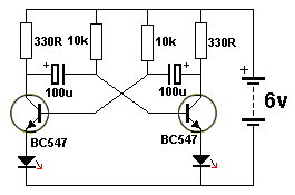
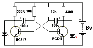
|
|
Fig 87. The
ASTABLE
("ay" - meaning not-stable) MULTIVIBRATOR circuit is rich in harmonics
and is ideal for testing amplifier circuits. To find a fault in
an amplifier, connect the earth clip to the 0v rail and move
through each stage, starting at the speaker. An increase in
volume should be heard at each preceding stage. This Injector
will also go through the IF stages of radios and FM sound
sections in TV's. |
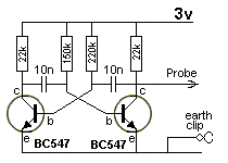
|
|
Fig 88. The astable
multivibrator can be made with PNP transistors. |
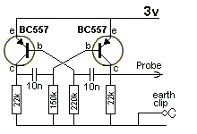
|
|
Fig 89. A circuit
can be made with one NPN and one PNP transistor. It ceases to be
a FLIP FLOP or Multivibrator as both transistor turn on at the
same time and the circuit becomes a Relaxation Oscillator. |
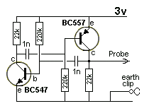
THE SINE-WAVE OSCILLATOR - also called the PHASE-SHIFT OSCILLATOR
A Sine-wave Oscillator can be made with a single transistor.
|
|
Fig 90.
This circuit produces a sinewave
very nearly equal to rail voltage. The important feature is the need for the emitter resistor and 10u bypass electrolytic. It is a most-important feature of the circuit. It provides reliable start-up and guaranteed operation. For 6v operation, the 100k is reduced to 47k. The three 10n capacitors and two 10k resistors (actually 3) determine the frequency of operation (700Hz). The 100k and 10k base-bias resistors can be replaced with 2M2 between base and collector. This type of circuit can be designed to operate from about 10Hz to about 200kHz. |
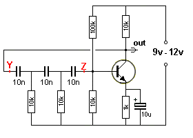
|
|
|
Fig 91. The phase-shift oscillator
has 3 "sections" made up of a 10n capacitor and 10k resistor.
This "section" is shown above and each
"section" produces a delay or "phase-shift" of about 60°
but the total must be 180°.
The base and collector of a common-emitter stage are 180° out-of-phase,
so the signal entering the base is 360° (IN-PHASE with the
output). This creates POSITIVE FEEDBACK. This concept is very hard to understand so we need to explain it in simple terms. Points Y and Z are the ends of a long piece of rope and the three resistors are weights tied to the rope. You shake the rope up and down at Y and Z moves up and down at a later time in the cycle. You know this because you can make a wave travel down a rope. Exactly the same thing happens with a signal that enters at Y. It takes time for the peak to reach Z. Now consider the circuit at switch-on. The caps are uncharged and the 10k collector resistor pulls the three capacitors high. Taking into account the voltage-dividing effect of the three lower 10k resistors, the collector is possibly at about 2v. The three 10k resistors start to charge the three 10n caps and the voltage on the base falls. This makes the collector voltage rise. This continues until the collector cannot rise any further and the capacitors continue to charge and the voltage on the base drops. The 100k base resistor takes over and starts to discharge the 3rd capacitor and turn the circuit on. The collector voltage drops and the energy in the three capacitors get passed into the base to fully turn the transistor ON. This all happens in a "sliding motion" that produces a sweeping output called a SINEWAVE. It is a very "delicate" oscillator and any change to the LOAD (10k) may stop its oscillation. How to read the Graph: Get a ruler and hold it "up and down" on the page (or on the screen) so you view the right-hand edge of the ruler and can only see the word "phase" and "60° " Now slide the ruler to the right and you will see the graph "A" gradually rising. Keep moving the ruler to the right and you will see graph "B" gradually rising. This is how you "interpret" the graph and see how graph "B" lags (is behind) graph "A." If you don't read the graph correctly, it looks like graph "B" is in front of graph "A" - but this is not the case. HOW THE CIRCUIT WORKS When the power is applied to the circuit the transistor will immediately turn on FULLY as the three 10n capacitors will acts as "short-circuits" and current will pass to the base and the collector voltage will fall to a very LOW level. The capacitors will gradually charge via the 10k resistors and the voltage across the second 10k resistor will drop (due to the charging current into the middle 10n gradually reducing) and the voltage on the left lead of the 3rd 10n will drop. This will reduce the voltage on the right lead of the 10n and turn the transistor OFF. The first two 10n's will start to charge but the voltage across the 2nd 10k will be very small and the 3rd 10n will start to charge via the 100k resistor. The charging of the first 10n is much faster than the charging of the third 10n and the voltage on the output rises to almost rail voltage. This allows the 3rd 10n to charge at a faster rate and just when the collector voltage reaches a maximum, the base voltage reaches 0.6v and the transistor starts to turn ON. This lowers the collector voltage but the transistor still keeps turning ON via the 100k and the three 10n start to charge. This action increases the "turn-ON" of the transistor and it continues to turn-ON until the voltage on the collector reaches a very LOW level. The circuit works completely differently to anything described in any Text Book. The transistor operates on a rising and falling CURRENT (increasing and decreasing current) into the base. That's why no-one has described it before. The third 10n continues to charge and the "turn-ON" current for the transistor reduces and it starts to turn OFF a slight amount. The second 10k continues to charge the middle 10n and the voltage across the 10k reduces. This pulls the left lead of the third 10n towards the 0v rail and the right lead follows. This action turns OFF the transistor and the collector voltage rises. REALITY Once you see how the circuit REALLY WORKS, it has nothing to do with 60° phase shift for each section between X and Y. No-one has actually sat down and worked out how the circuit works and they just copy mistakes from others. The overall DELAY produces a signal that ASSISTS in keeping the circuit oscillating, but the feedback signal is not a simple sinewave. It's possibly NOT important how the circuit works, but when you have trouble seeing how a 10n and 10k can produce a 60° phase shift, you have to look into the circuit and satisfy yourself. You cannot possibly expect to fault-find a circuit if you don't have an understanding of how it works. Things you will learn in one circuit can be applied to another circuit and this is how you progress. That's why the operation of this circuit ahs been provided and is completely different to anything that you would have considered. |
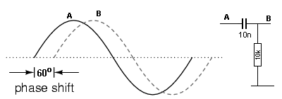
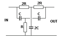
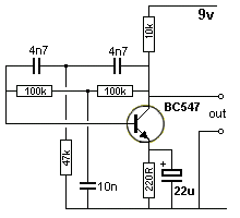
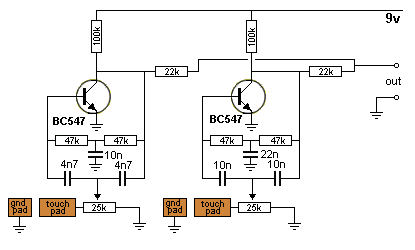
THE BLOCKING OSCILLATOR
|
|
Fig 92. The BLOCKING
OSCILLATOR circuit uses a transformer to produce POSITIVE
FEEDBACK to the base. The circuit starts by Rbias charging Cbb to deliver voltage to the base of the transistor via Rb (and also a small current). The transistor turns on and produces expanding magnetic flux in the primary of the transformer. This flux cuts the turns of the secondary (or feedback) winding and increases the base voltage and CURRENT. The voltage out of the top of the secondary winding is prevented from "disappearing" by Cbb. The transistor keeps turning ON until it cannot turn on any more. At this point, the current through the primary is a maximum but it is not expanding flux and its effect is not passed to the secondary winding. The base-current reduces enormously to the very small Rbias current and the transistor turns off abruptly (it takes a high base current to maintain a high collector current and the base current is very small). The heavy current through the primary is producing a very strong flux and it collapses, producing a voltage in both windings of opposite polarity and very high amplitude. Fig 92a shows the base being "capacitor injected." This saves one resistor and can produce a higher output. All the values and the transformer needs adjusting for the performance required. The start of each winding is shown with a dot. This assumes the windings are wound in the same direction. Figs 92b,c shows alternative ways to produce a blocking oscillator. The difficulty with producing a Blocking Oscillator is getting a suitable transformer. 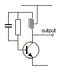 Fig 92c |
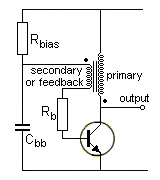
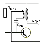
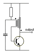
|
|
Fig 93. A simple
BLOCKING OSCILLATOR circuit can be made with a 10mH inductor
and 80 turns of very fine wire wound on top. The piezo diaphragm reacts to the very high "FLYBACK VOLTAGE" produced by the primary when the transistor turns off. This type of circuit is often used to produce very high voltages. |
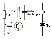
|
|
Fig 94. This LED
Torch circuit uses the "flyback" voltage of a BLOCKING
OSCILLATOR to illuminate a 3.6v super-bright LED from a 1.5v
supply. Note: the 10n capacitor prevents the energy from the feedback winding being lost. All the energy from the feedback goes into the base of the transistor to turn it on hard. |
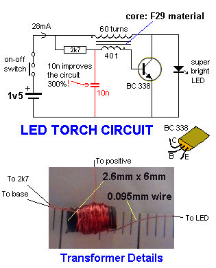
|
|
Fig 95 shows a Blocking Oscillator producing a regulated 5v from a 1.2v supply. |
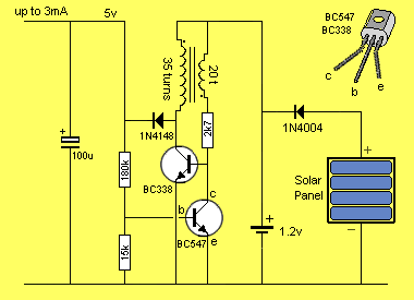
|
|
Fig 96. A simple
extension of the Blocking Oscillator in Fig 92c above, is shown in this
diagram. It consists of two BLOCKING OSCILLATOR transistors that
are turning each other off. The circuit starts by one transistor
being slightly faster than the other. It turns ON and produces
magnetic flux that cuts the turns of the other half of the
primary winding to increase the voltage from the battery and at
the same time it reduces the voltage to the base of the other
transistor - because the transistor allows only a very small
voltage to appear across the collector-emitter terminals when it
is turning ON. It keeps turning on until it is fully ON. At this point the flux is no longer expanding and the generated voltage in the winding that supplies the base voltage (and current) ceases. This turns it off a small amount and the magnetic flux starts to collapse and produce voltages in the opposite direction. The voltage (and current) to the base is less than before and this turns the transistor off more. The voltage to the base of the other transistor starts to rise and that transistor takes over. The two transistors operate in PUSH-PULL mode. To reduce the wasted power in the 220R resistors, Fig 96a uses Darlington transistors and 2k2 0.5watt resistors. The circuit is used to drive a CFL lamp from a 12v battery. |
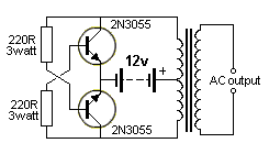
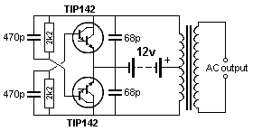
The difficulty with producing a Blocking Oscillator is getting a suitable transformer. A similar "flyback voltage" can be obtained from an inductor. This will need an oscillator made up of two transistors to drive the inductor.
|
|
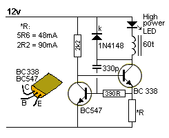
|
Fig 97.
This circuit is a "Buck Converter" meaning
the supply is greater than the voltage of the LED. It will drive one
high-power white LED from a 12v supply and is capable of delivering 48mA
when R = 5R6 or 90mA when R = 2R2.
The LED is much brighter when using this circuit, compared with a series
resistor delivering the same current. But changing R from 5R6 to 2R2 does not double the brightness. It only increases it a small amount. The inductor consists of 60 turns of 0.25mm wire, on a 15mm length of ferrite rod, 10mm diameter. Frequency of operation: approx 1MHz. This circuit draws the maximum current for a BC 338. When the circuit is turned on the 330p gets charged. This turns on the BC547 and keeps the BC338 off. When the 330p is charged the BC547 is not turned on as much and the 2k2 can start to turn on the BC338. It pushes the charge on the 330p into the base of the BC547 to keep it off. The 330p gets discharged by the 330R and the voltage across the *R resistor turns on the BC547 to turn off the BC338. The 1N4148 absorbs the high-voltage flyback pulse. The circuit is only active for a very short period of time and off for a longer period of time. This delivers a small amount of energy to the high powered LED and allows the LED to be connected to a 12v supply (via the circuitry). |
|
|
A flyback oscillator is any oscillator where the transistor turns off quickly and abruptly during part of the cycle and allows the energy (the flux) in an inductor to collapse suddenly to produce a high voltage IN THE OPPOSITE DIRECTION. The circuit in Fig 97a consists of a transformer with a feedback winding of 40 turns. It can be constructed as a piece of test equipment to test transistors, zeners and LEDs. |
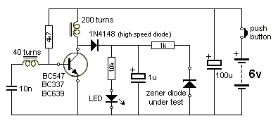
|
|
FLYBACK OSCILLATOR This circuit is a very good example of a flyback transformer in operation. The CFL needs a very high voltage to strike (start the illumination) when the anodes (all projections into a glass tube are called anodes) are not heated. You cannot use the "turns- ratio" (50:500 in this case) to determine the output voltage because the transformer is used in its "collapsing mode." |
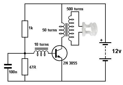
|
|
This circuit will drive
a 5watt CFL tube from an old CFL lamp from 6v or 12v. It makes a
very handy emergency light. The transformer is made by winding 500 turns for the secondary. This consists of winding about 10 turns on top of each other before advancing along the rod. The rod can be round or flat, from an old AM radio. It is called a ferrite rod. The 500 turns have to be added before reaching the end and this means 100 turns has to take up 1/5th of the distance. This reduces the voltage between the turns as the enamel will only withstand 100 volts. Before you start winding, use at least 3 layers of “sticky-tape” to prevent the high voltage shorting to the rod. The size of the wire is not important and anything 0.25mm or thinner will be suitable. After winding the secondary, the primary is 50 turns and the feedback is 10 turns. The primary can be 0.5mm wire and the feedback 0.25mm. Connect the transistor, components and tube and turn the circuit ON very briefly. If the tube does not illuminate immediately, reverse the wires to the feedback winding. The transistor must be 2N 3055 (or the plastic version, TIP 3055). It will get warm when illuminating the lamp and needs to be heatsinked. The lamp must not be removed as the circuit will overload and damage the transistor. The circuit takes 250mA when driving a 5 watt CFL (or 18 watt fluorescent tube) on 12v supply. The 1k base resistor can be reduced to 820R and the brightness will increase slightly but the current will increase to 500mA. The circuit is more-efficient on 6v. The 1k base resistor is reduced to 220R and the transistor remains cool. |
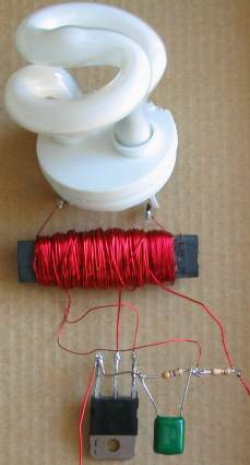
THE BOOST CIRCUIT or BOOST CONVERTER
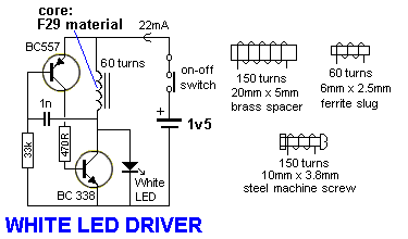
Fig 97aa
Any circuit
that converts a low voltage to a higher voltage is classified as
a BOOST CONVERTER or BOOST CIRCUIT.
Fig 97aa will
drive a super-bright white LED from a 1.5v cell.
The 60 turn inductor is wound on a small ferrite slug 2.6mm dia
and 6mm long with 0.25mm wire.
The main difference between this circuit and the two circuits
above is the use of a single winding and the feedback to produce
oscillation comes from a 1n capacitor driving a high gain
amplifier made up of two transistors.
The feedback is actually positive feedback via the 1n and this
turns on the two transistors more and more until finally they
are fully turned on and no more feedback signal is passed though
the 1n. At this point they start to turn off and the signal
through the 1n turns them off more and more until they are fully
turned off.
The 33k turns on the BC557 to start the cycle again.
THE BUCK CONVERTER
We are going to lump all these oscillators together as they are
variations on a similar design. There are two common oscillators that
can be recognised by the layout of the circuit.
The Colpitts oscillator has 2 capacitors across the coil with the signal taken
from the join or it may have a tuned circuit with the signal taken from
the active end. The Hartley Oscillator has a tapped coil
and these are difficult to obtain.

Fig 97bAny circuit
that converts a high voltage to a lower voltage is classified as
a BUCK CONVERTER.
Fig 97b will drive
a 1watt white LED from a 12v supply and is capable of delivering
300mA. The driver transistor is BD 327 and the inductor is 70
turns of 0.25mm wire wound on the core of a 10mH inductor.
The voltage across the LED is approx 3.3v - 3.5v
The 1R is used to measure the mV across it. 300mV equals 300mA
LED current.
The diode MUST be high speed. A non-high-speed diode increases
current 50mA.
This circuit is a very good design as it does not put peaks of
current though the LED.
The Armstrong, Clapp, Colpitts, Hartley, Wien Bridge and even
unknown oscillators like the one below all use capacitors, resistors and
coils to create a circuit called a RESONANT CIRCUIT and these two
components produce a sinewave when they receive a pulse of energy.
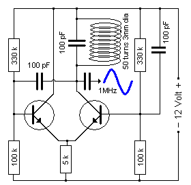
Fig 98.
|
|
|
|
|
|
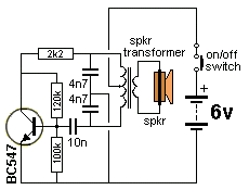
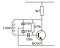
|
|
|
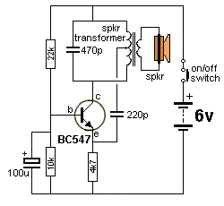
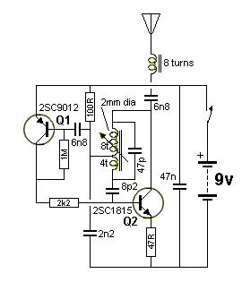
|
|
|
DOOR-KNOB ALARM This circuit can be used to detect when someone touches the handle of a door. A loop of bare wire is connected to the point "touch plate" and the project is hung on the door-knob. Anyone touching the metal door-knob will kill the pulses going to the second transistor and it will turn off. This will activate the "high-gain" amplifier/oscillator. The circuit will also work as a "Touch Plate" as it does not rely on mains hum, as many other circuits do. The first transistor is a Colpitts Oscillator and the feedback is via the 47p. Explaining the operation of this oscillator could take a page of discussion. We are only going to explain one amazing feature - how the oscillator creates the second half of its cycle. We know how the stage turns on (via the base-bias resistor) - but how does it turn OFF to create the other half of the waveform. Here's how: We know that when a transistor turns ON, the collector voltage falls and the emitter voltage rises. Simply joining these two points with a resistor or capacitor will not produce feedback as one is falling and the other is rising. We need to join two points that are rising AT THE SAME TIME. The secret comes from the inductor. The 16 turns of wire produces a voltage in the opposite direction when the transistor is turned off. In the first diagram of fig 103b we see the transistor turned ON and current flows through the coil. The voltage at the bottom of the coil will be slightly lower than the supply voltage. When the transistor is turned off, it is effectively out of the circuit and the current flowing through the coil produces magnetic flux that will collapse very quickly and produce a voltage across the ends of the coil that will be OPPOSITE to the applied voltage. This means the voltage at the bottom of the coil will be HIGHER than rail voltage and we can think of the coil rising above the power rail and producing a voltage 2, 5, 10 or even 100 times higher than the power-rail voltage. This is the amazing fact about a coil (inductor) and is the secret behind the operation of this circuit. |
|
|
|
In circuit 103b, this high voltage is produced at some
point in the cycle and it pulls the emitter UP a small amount via the
47p and this turns the transistor OFF. We are not going into what part
of the cycle produces the high voltage via the inductor but it DOES.
That's how the circuit produces the second part of its cycle. The inductor produces
a high voltage that starts to turn off the transistor and this allows
the inductor to produce a higher voltage and the transistor is turned
off even more. During this time the 47p feedback capacitor is charging
and RISING. Most oscillators are described on the web and you can decide which type you need for your particular application. |
|
|
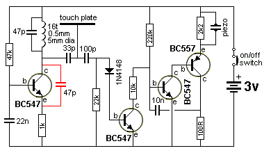
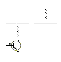
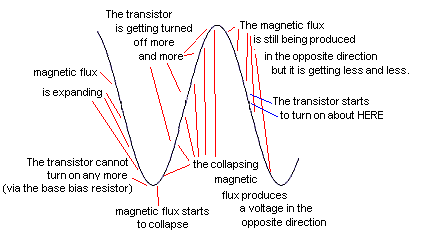
| Every electronic component has a
value of resistance. You can measure this value with a
multimeter. But sometimes the value changes according to the
light it receives, the frequency it is operating-at, or the
voltage it is connected-to, or the sound it receives, or its
temperature or many other influences. Sometimes the output from a circuit might be 2v, but if you put a low-impedance device such as a speaker on the output, it "kills" the sound. Or you may have a nearly flat 9v battery. It measures 5v with a multimeter but when you connect a 3v motor, it does not work. These are both examples of poor IMPEDANCE MATCHING - yes, the battery has a HIGH Impedance and that's why it cannot deliver the current required by the motor. What is IMPEDANCE MATCHING? Impedance Matching is is connecting two items together so: "THEY WORK." Some devices PRODUCE or DELIVER a signal or a voltage or a current. Some devices ACCEPT a signal or voltage or current. We need to connect these types of devices together. Let's start with those that DELIVER: An amplifier may be able to produce an output of 2v, but when a low-impedance device (low resistance device) such as a speaker is connected, it cannot deliver the CURRENT needed to drive the speaker. The same with a flat 9v battery. It cannot deliver the CURRENT needed to drive a 3v motor. You cannot "test" or measure the output capability of a device. You must connect it to the input of the project you are designing and measure the waveform or voltage being delivered (or transferred). If the voltage or waveform is considerably less than when it is not connected, you have decide if the attenuation (reduction) is acceptable. The ideal situation is NO attenuation - but in nearly all cases you will get some attenuation. There are no "rules to follow" and every case is different. However when the output of a device is NOT reduced when it is connected to a circuit, the two items are said to be IMPEDANCE MATCHED. There are three ways to "Match Impedances:" 1. via a resistor. This is generally a poor way to match impedances and is very inefficient. But it may be the only way to connect two devices. 2. via a capacitor. This can be a very good way to match impedances. 3. via a transformer. Generally the most efficient way to match impedances but requires a lot of calculation and expense in getting the transformer designed and manufactured. Impedance Matching can also be referred to as "MATCHING" and the simplest example is connecting a 6v globe to a 12v battery. This is called "Resistance Matching" or "Current Matching" or "Voltage Matching" because the resistance, voltage and current are known quantities. [To connect a 6v globe to a 12v battery you can use a resistor or put two 6v globes in series. Using a resistor will be very difficult because a globe requires about 6 times normal current to allow it to start illuminating and then it takes the "rated current."] But when when a device produces a signal; the voltage, resistance and current changes during the production of the signal and because these values are not constant, we use the term IMPEDANCE MATCHING. Impedance really means "resistance that changes during the production of the waveform." Impedance matching can be worked out mathematically, but you need to know all the parameters of the device and the circuit you are connecting together. This is rarely possible to obtain. Rather than calculate the result, it is much easier and more-accurate to connect the two items and view the result on a CRO (Cathode ray Oscilloscope). But if you cannot do this, simply connect them and listen or view the output from a speaker, relay or LED etc. We have already studied "Impedance Matching" in the circuits above, but did not identify the concept. We will now go over some of the circuits and show where impedance matching took place:
|
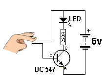
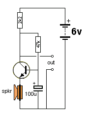
|
SATURATING A TRANSISTOR This is the last topic for discussion because it is the last thing to attend to when designing a circuit. We have explained the fact that a transistor turns ON when the base voltage is above 0.7v and the current though the collector-emitter leads is approximately 100 times the base current. This means a transistor with a gain of 100 will deliver 100mA to a collector LOAD when 1mA enters the base. This is theoretically true and will occur in nearly all cases, but some devices such as motors and globes need a lot more current to get them started or to get them to turn ON because the cold resistance of a globe is only about 1/5 its hot resistance. This means a 100mA globe needs 500mA to get it to start to glow. The same with a motor. The starting or "stalled current" is 5 times more than the operating or "running current. On top of this the transistor might not have a gain of 100 and the voltage may be slightly higher than expected. All these things means the transistor must be turned ON with more than 1mA into the base. If you deliver 2mA, it does not mean the transistor will deliver 200mA to a LOAD. If the load requires 100mA, delivering 2mA to the base will simply turn the transistor ON harder and the collector-emitter voltage will be slightly lower, but the load will still draw (or take) 100mA. But the devices we mentioned above require 500mA to get them started, so the base current needs to be 5mA. Now, here's the unfortunate part, 5mA base-current will not deliver 500mA collector current. The transistor needs more than 5mA base-current to get it to deliver this HIGHER current. It needs about 7mA. This process can be proven by experimentation. Simply increase the base current until the device is turned ON, then measure the base current. Add 1mA to 3mA to guarantee reliability and the circuit is complete. This process is called SATURATING A TRANSISTOR or GUARANTEEING TURN-ON, or FULLY SATURATING the TRANSISTOR or FULLY TURNING the TRANSISTOR ON. HYSTERESIS (see also Schmitt Trigger above) Hysteresis is a feature of a circuit. It is when the circuit turns on at a particular voltage and turns off when a higher or lower voltage is reached. The gap between these two voltage-levels is called the HYSTERESIS GAP. This is a very handy feature. It prevents an effect called "hunting." If a circuit turns on at say 6v, and turns off at 5.7v, any slight variation in the supply voltage will cause the output to change state. This may produce an undesirable effect of the circuit turning "on and off" at the wrong time due to supply voltage fluctuations. By increasing the gap between these two voltages, the circuit will remain in one state or the other - until the input voltage (the controlling voltage) increases or decreases. The Schmitt Trigger (Fig 79a) is an example of a circuit using Hysteresis. Any circuit with a positive feedback line, introduces the effect we are talking about. The feedback line has the effect of assisting the input voltage. In other words, it widens the gap between an ON state and an OFF state. This is called POSITIVE FEEDBACK because it ADDS to the effect of the input voltage. Even when the input voltage is falling, the feedback improves the ON or OFF state by taking the circuit past the point where the change takes place. Rather than thinking of the feedback as "positive," consider it as AIDING. All HYSTERESIS feedback is AIDING or ASSISTING the effect you are trying to produce. This circuit uses Hysteresis. The main "assisting component" is the 22k. |
|
|
| This is how the circuit works: When the circuit is turned on, the base of the second transistor gradually develops 0.6v and the transistor turns ON. The voltage between collector and emitter is about 0.2v and the third transistor is OFF. When the first transistor receives an AC signal, an increasing voltage on the base causes the collector voltage to reduce and the charged 4u7 electrolytic moves towards the 0v rail. The negative lead of the 4u7 goes below the 0v rail by about 0.6v. This allows the second diode to discharge the 10u electrolytic and the 0.6v on the base of the second transistor is reduced. Let's say it is reduced to 0.55v. This causes the second transistor to turn off and the positive lead of the 1u electrolytic rises toward the 12v rail. The negative lead of the 1u rises too and this makes the transistor turn ON. In this process the 1u starts to charge and it has the effect of slowing down the "turning ON" of the second transistor. But the pulses keep coming from the first transistor and 10u is kept discharged. The 1u keeps charging and eventually it is fully charged and now the pulses from the first transistor can finally turn off the second transistor. The third transistor is turned ON and the 22k connected to the collector of the third transistor reduces the voltage on the base of the second transistor by about 0.15v This helps the pulses from the first transistor to keep or put a low voltage on the base of the second transistor and even if these pulses stop, the voltage on the base will take time to rise via the 15k and this is called the HYSTERESIS GAP. When the circuit changes state, the pulses from the first transistor will discharge the 10u and this will be "fighting against" the 15k and 22k resistors that will be trying to charge the 10u. |
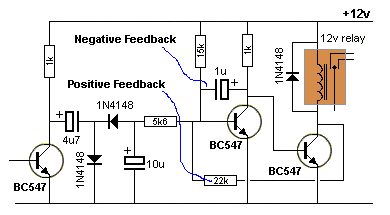
| The circuit
shows a capacitor between the base and collector. It provides
NEGATIVE FEEDBACK. If we remove the capacitor, when the base "moves down," the collector "moves up." In other words the signal is inverted. When the capacitor is fitted, we have to start with the collector because it has more "power" and it is the lead that is driving the action of the capacitor and then go to the base. When the collector voltage "moves down" the right plate of the capacitor moves down and it charges and tries to pull the left plate down too. |
|
|
This is the
opposite effect to the signal moving through the transistor.
This means the capacitor is working against
the action of the transistor.
The capacitor will have more effect on high
frequency signals while the low-frequency signals will be
affected less. Because the capacitor is working against the natural flow of signal through the circuit, it is called NEGATIVE ACTION or NEGATIVE FEEDBACK. |
|
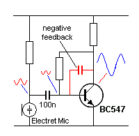
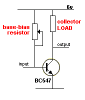
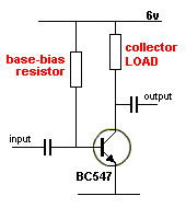
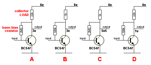
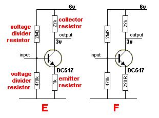
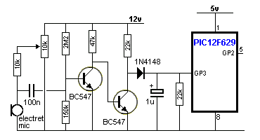
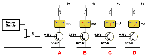
|
LEAKAGE This topic covers small, unwanted, currents produced when two or more transistors are connected together. |
|
|
|
In the Faulty
Headlight Extender Circuit we see 3 transistors directly
connected together. When the 100u discharges, the BC547 turns OFF and this turns off the BC557 and also the BD679. But the relay remains activated. This is due to the BC547 not turning off fully and a very small current flows though the collector-emitter leads. This current is amplified by the BC557 (about 200 times) and then by the BD679 (about 20,000 times). The resulting current is sufficient to keep the relay activated. Two resistors are needed to turn the circuit off. The 100k on the base of the first transistor discharges the 100u and makes sure the voltage on the base is zero so the transistor is fully turned off. The 2k2 on the base of the BD679 does not remove the slight leakage current though the BC557 but it flows through the 2k2 and this produces a very small voltage-drop, that is too small to turn on the BD679, and this makes sure the BD679 turns off. This type of problem will occur whenever two or more transistors are directly coupled together. Even a leakage current of less than 1microamp will amplify to many milliamps with the gain of two or three transistors. See more on leakage in Spot the Mistake P27 Leakage. |
| High-side Vs Low-side Switching | |
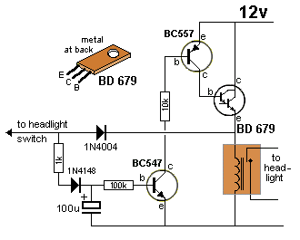
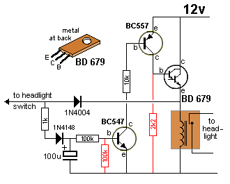
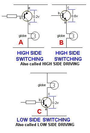 |
Devices such as globes, motors, relays etc are called
LOADS. They can be placed above or below the driver transistor. When the
driver transistor is above the load, as shown in diagrams A and B the circuit is called HIGH-SIDE
SWITCHING. When the driver transistor is below the load, as shown in
diagram C, the circuit
is called LOW-SIDE SWITCHING. The circuit for low-side switching is much easier to design and can be less expensive however high-side switching is the only arrangement available in cars and trucks as the load (globes and motors ) are generally connected to chassis (to save wiring) and the control wire (power wire) comes from the positive of the battery. For the HIGH-SIDE SWITCHING, the control line (the input to the base) can be active LOW (as in the first diagram). In the second diagram, the base is taken HIGH and the emitter follows. The voltage across the collector-emitter terminals will be higher than the fist example and the transistor will get hotter. This is because the base of the NPN transistor cannot rise above the supply (in most cases such as cars and trucks) and the voltage between collector and emitter will be about 0.65v. |
| The three diagrams above show the
voltage across the collector-emitter leads when the transistor
is fully conducting. In diagram B the transistor is an emitter-follower and the voltage is three times larger than diagrams A and C. This means the heat generated by the transistor will be three times larger than diagram A or C. |
|
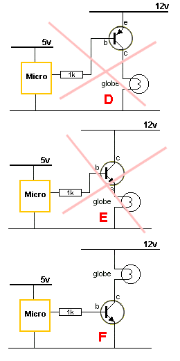 |
Diagram D
shows the problem trying to switch a load on a 12v supply, from
a 5v microcontroller. When the microcontroller is HIGH, the
voltage is not high enough to turn off the transistor. The
voltage on the base must be nearly 12v for the transistor to
turn off. This circuit will NOT WORK. In diagram E, the voltage on the base will only rise to 5v, and thus the globe will see only 4.4v and will not illuminate fully. The transistor will get fairly hot. The solution is to drive the LOAD via LOW SIDE SWITCHING as shown in diagram F. It is possible to switch a HIGH SIDE transistor from a microcontroller by including a zener diode so the transistor is turned off when the microcontroller is HIGH. The 10k resistor makes sure the base sees 12v when the micro is HIGH. The voltage of the zener is chosen so that when the micro is HIGH, the micro rail voltage, plus the voltage of the zener is more than the supply to the globe.
|
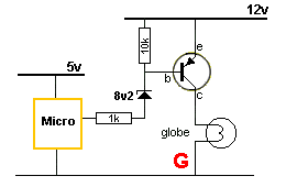
This sounds very complex but it is very simple.
The simplest voltage-to-current component is a resistor.
A resistor performs lots of different jobs, depending on the circuit.
One of its jobs limits the current to a LED. It is called a CURRENT LIMITING RESISTOR. It can also be called a VOLTAGE TO CURREN2ONVERTER.
Here's how it works:
|
A resistor is a VOLTAGE TO CURRENT CONVERTER |
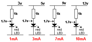
A red LED must be delivered a voltage of exactly 1.7v for it to work. In
other words it must be connected to a 1.7v supply.
But a 1.7v supply is very hard to obtain, so we use a 3v supply and a
dropper resistor.
The resistor converts the 3v to 1.7v.
This is easy to understand because the 3v supply is fixed at 3v and when
a voltage is delivered to the red LED it develops exactly 1.7v across
it. The resistor sits between the 3v and 1.7v
When the voltage of the supply is increased, The voltage across the LED
remains at 1.7v and the voltage across the resistor increases. This is
shown in the diagrams above.
When the voltage across a resistor increases, the current through it
increases. That's how we get 3mA, 7mA and 10mA. This is called VOLTAGE
TO CURRENT CONVERSION.
The VOLTAGE on the input goes up and down and the CURRENT through the LED
goes up and down.
The input CURRENT will also go up and down but we are only covering the
fact that the input VOLTAGE rises and falls and the output CURRENT RISES
and falls.
Any circuit that produces this effect is called a VOLTAGE TO CURRENT
CONVERTER.
A transistor can also be connected to produce VOLTAGE TO CURRENT
CONVERSION.
The following circuit is an emitter-follower. It is also a VOLTAGE TO
CURRENT CONVERTER. A rising and falling voltage on the input
creates a rising and falling CURRENT on the output.
It also produces a rising and falling voltage on the output but we are
only concerned with the fact that the circuit produces a rising and
falling CURRENT on the output when the input VOLTAGE rises
and falls.
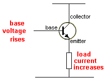
An
emitter-follower is a VOLTAGE TO CURRENT CONVERTER
The circuit in Fig103e requires say 1mA input current. The output current will be
100mA. The circuit has the capability of increasing the current or
AMPLIFYING the current. The resistor circuit above does not AMPLIFY the
current. It is only a voltage-to-current converter.
The transistor performs a VOLTAGE TO CURRENT CONVERSION and also
produces CURRENT AMPLIFICATION.
A common-emitter stage also performs VOLTAGE TO CURRENT CONVERSION.
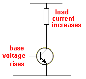
Fig 103f.
A common-emitter stage
is a VOLTAGE TO CURRENT CONVERTER
A slight increase in the voltage on the base of a common emitter
transistor will increase the current through the load by a large amount.
As you can see, there are lots of circuits that perform VOLTAGE TO
CURRENT CONVERSION but we usually identify them for other features and that's
why the term VOLTAGE TO CURRENT CONVERSION is rarely mentioned.
There are also special circuits (using op-amps) to perform precision
voltage-to-current conversion, but we are concentrating on transistor
stages.
ANOTHER VOLTAGE TO CURRENT CONVERTER
Here is another
VOLTAGE TO CURRENT CONVERTER:
A photo detector (A light dependent resistor - LDR) produces a very wide
change in resistance from dark to light conditions and when it is
connected to a LOAD RESISTOR, the voltage across this resistor will
change considerably.
But we cannot use this voltage-change to directly illuminate a LED or
drive a motor because it does not have enough current. We need to
convert this voltage-change to CURRENT-CHANGE.
The current through the resistor might be up to 1mA. A motor or LED or
relay needs 10mA to 300mA.
Here is what we have:
We have a wide (large) change in voltage and require this to be
converted to a wide change in current.
We say this voltage-change has very weak driving capability because it
will not illuminate a LED or anything else.
We want a POWERFUL DRIVING CAPABILITY and that's what a CURRENT DRIVER
is capable of doing.
In other words we want to convert a WEAK driver to a POWERFUL
driver.
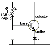
When light falls on the LDR, the voltage across the resistor increases
and this voltage-rise is detected by the base of the transistor and a
small current passes into the transistor. The transistor amplifies this
current and delivers up to 100 times more current to the circuit created
by the collector-emitter terminals. The LED is in this circuit and the
LED will illuminate brightly when 5 to 25mA flows. This is only a
demonstration circuit to show the effect of shining a light on the LDR.
It may cause the LED to shine too bright and be damaged as no
current-limiting resistor has been included to protect the LED.
CURRENT
TO VOLTAGE CONVERTER
A resistor can be used
as a CURRENT TO VOLTAGE CONVERTER.
Fig 103g shows a resistor called a SENSE RESISTOR.
It is a low-value resistor in series with one line of a circuit and its
function is not to change the operation of the circuit in any
way.
|
|
When a current flows though a resistor, a voltage is produced across the resistor. You can also say a VOLTAGE DROP is produced across the resistor. If the resistor is exactly 1 ohm, a voltage of 1v will be produced across it when 1 amp is flowing or 1mV is produced for each 1mA of current. Using a 1 ohm resistor produces an easy conversion.
If the circuit is 24v or 50v, a loss of 1 volt will not be noticed.
But if the circuit has a lower voltage, (say 5v) the resistor will be need to be a lower value so the drop across the sense resistor does not upset the operation of the circuit.
The actual value of the resistor is not important for this discussion, It can be 1 ohm or 0.1 ohm.
The important point is to understand the function of a Sense Resistor.
In the circuit above, if the globe is replaced by a 20watt or 50watt, globe, the current through the sense resistor will increase. We measure the voltage (in millivolts) across the resistor and we convert the value into CURRENT. This is a CURRENT to VOLTAGE CONVERSION.
A transistor can be used as a CURRENT TO VOLTAGE detector. Fig 103h shows a 1 ohm sense resistor connected to a transistor. When the circuit is turned ON, the charging current (the current flowing into the battery) will be high and when the voltage across the sense resistor reaches 0.65v, the transistor turns ON and the voltage on the collector reduces. This turns on the red LED and reduces the voltage on the ADJ terminal of the LM317T regulator and the regulator outputs a lower current to the batter. This is how the circuit limits the charging current. The resistor is converting the current flowing through the circuit (and into the battery) into a voltage, and the transistor detects the voltage. The transistor is not detecting or measuring the current. It has absolutely no idea of the amount of current flowing. It is detecting the voltage across the resistor. The resistor is performing the CURRENT to VOLTAGE conversion.
|
|
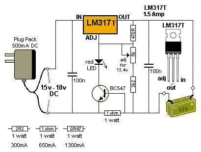
SQUEALING, BUZZING, OSCILLATING,
This effect can be reduce and eliminated by a term called DECOUPLING.
and MOTOR-BOATING
We have studied POSITIVE FEEDBACK
and the effect it produces. It turns an amplifier into an
oscillator.
The following circuit will not work:
The three stages of amplification will
produce so much gain that the circuit will self-oscillate. The output
will be a "buzzing-sound" and the fault will be impossible to find
because it comes from within the design of the circuit. The first
thing you must do is add "power-supply decoupling."
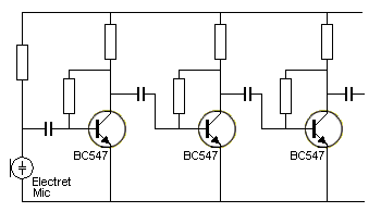
Fig 104a.
The unwanted sound produced by the circuit is called MOTOR-BOATING and is
generated in the "front-end" by very
small noises or "disturbances" and amplified by the stages that follow.
Fig 104b shows where the noise starts. It can be produced by the
electret microphone or by the noise in the junctions of the first
transistor (due to current flowing in the collector-emitter circuit).
This waveform will be very small and almost impossible to detect via any
test-equipment, but it will start in the first stage and pass through the
coupling capacitor as shown in Fig 104c.
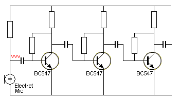
Fig 104b.
The next stage will amplify this "noise" and it will be amplified
further by the following stages.
There will be some slight cancellations from the various stages as the
signal will be "out-of-'phase" but the end result will be a
"putt-putt-putt" or squealing from the output.
The general term for this is called MOTOR-BOATING and is due to
the high gain of the circuit.
The noise will appear on the power rail and get passed to the front-end
where it will be amplified more.
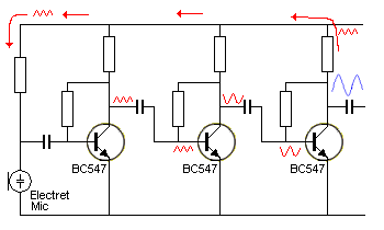
Fig 104c. The positive feedback loop producing "Motor-boating"
Decoupling is achieved by adding capacitors [electrolytics] (and
resistors) across the power rails so that each stage is effectively
powered by a separate supply.
Adding an electrolytic can sometimes make a big difference and sometimes
it will make no difference.
It all depends where it is connected and the value.
Fig 104d shows an electrolytic connected across the power rails.
This is called DECOUPLING THE POWER RAILS and effectively
tightens up the power rails so that any noise on the positive rail is
removed.
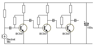
Fig 104d.
But, as you can see, the power rails extend to the first
transistor and although the rails may be "tight" near the battery they
can "move" near the first stage.
This is due to the wiring between the stages or the tracks on the PC
board. That's why an electrolytic across the battery may have little
effect on removing our motor-boating problem.
Fig 104e shows an electrolytic connected across the supply that
feeds the
electret microphone and 1k2 resistor to separate the supply we have just
created, from the main supply rail.
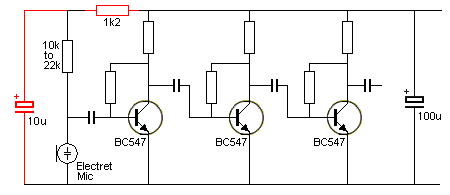
Fig 104e.
We have effectively created a separate power supply. It is fed by a 1k2
and kept "tight" by the 10u capacitor.
The electrolytic does not have to be a high value because the electret
mic takes very little current and the voltage-waveform (the AC signal)
produced by the microphone is very small (about 20mV).
These two items very effectively decouple the microphone from the supply
rails so the microphone has its own supply. The 1k2
resistor does most of the "separation." The voltage-drop across it will
be very small and it will not affect the operation of the circuit, but
the small voltage-drop will prevent any noise on the power rails being
fed to the microphone via the 10k resistor.
To remove any slight motor-boating problems (if they still exist); a
power-supply filter (called power-supply decoupling) made up of a 1k2
and 10u can be placed after the first amplifier stage as shown in
Fig 104f.
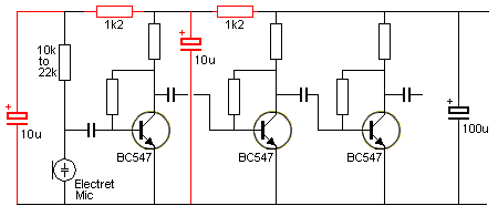
Fig 104f.
By selecting the value of capacitance and resistance, this arrangement
will remove almost all motor-boating problems. It is
a very-effective form of suppression.
Decoupling is most-effective on the pre-amplifier stages, however every
circuit is different and these two components only deal with the
low-frequency motor-boating type of instability. Some circuits also
produce high-frequency oscillations (about 1MHz) and these need removing
by a different value of capacitor-feedback.
BREAKDOWN and ZENER MODE
There are two conditions or
states where a transistor can be instantly damaged. This is due to
voltage applied in the wrong direction or the application of voltage
that is higher than the rating of the transistor.
Voltage will kill a transistor faster than excess current.
A high voltage spike can damage a transistor instantly.
However if the excess voltage does not have enough current to damage the
transistor, it will recover and we can use this feature in a circuit.
Breakdown and zener mode are different.
In breakdown mode, suppose we have a transistor that has a
specification of 85v for the voltage it will withstand between the
collector and emitter as shown in Fig 104g:
It will "resist" a voltage of
85v and this voltage will appear
across the collector-emitter leads. When the voltage increases to 86v,
87v ... the transistor will suddenly breakdown and only a few volts will
appear across it. This fires the trigger transformer in the circuit
above.
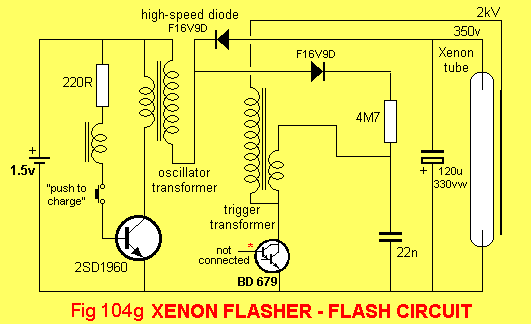
If the current is very small, the transistor will not be damaged and
when the voltage is removed and a lower voltage applied, it will operate
as an undamaged device.
In zener mode, the base-emitter junction is connected to a
voltage higher than 9v via a resistor. The junction will breakdown and a
voltage of about 7v will appear across the base-emitter leads and the
excess voltage will be dropped across the resistor.
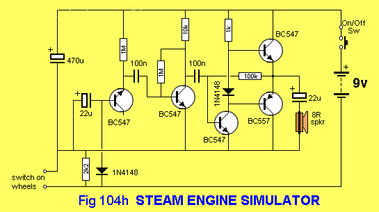
The zener-effect or zener mode can be used to produce white noise or a
7v zener reference.
Fig 104h shows the first transistor with the base-emitter
junction reverse-biased to produce a "noisy zener" via the 1M feeder
resistor. The noise is picked off via the 100n and amplified by the
remainder of the circuit.
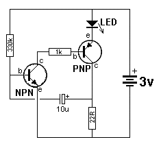 |
This circuit is basically a high gain
amplifier with feedback that causes the LED to flash at a rate
determined by the 10u and 330k resistor. Remove one of the transistors and insert the unknown transistor. When it is NPN with the pins as shown in the photo, the LED will flash. The circuit will also test PNP transistors. To turn the unit off, remove one of the transistors. |
|
|
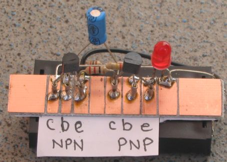
ZENER TESTER
The maximum voltage a transistor can withstand is called the ZENER VOLTAGE of the transistor.
It is Vce - the voltage between (across) collector and emitter. It is also the maximum supply voltage or circuit voltage or the voltage generated by an inductor in the collector-circuit and can be tested via the following circuit. This circuit will also test ZENER DIODES and LEDs.
|
|
|
|
The circuit is a
flyback oscillator. This type of
oscillator energises an inductor then turns off very quickly and
the magnetic field (flux) produced by the inductor collapses and
produces a very high voltage in the opposite direction. The
maximum voltage produced by the circuit depends on the "maximum
voltage capability" of the transistor. The voltage produced by the inductor is over 120v but the transistor will zener at a voltage lower than this and thus the output voltage will be determined by the characteristic of the transistor. A diode on the output of the inductor passes this high-voltage-spike to a 1u electrolytic, which stores the energy and provides a high voltage output. The circuit will test transistors up to 120v and zeners up to the voltage produced by the transistor. The project is built on a strip of PC board cut into lands with a file or saw. The following diagrams shows the parts placement and connecting the 5 button cells to the board. The project can be built in an evening and added to your TEST EQUIPMENT.
|
|
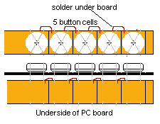 |
TESTING A
TRANSISTOR When testing a transistor, fit it into the pins marked C B E. If you have a LED connected to the LED terminals, it will glow. If you remove the LED and measure the voltage across the 1u electrolytic, it will provide the maximum working voltage for the transistor. TESTING A ZENER When testing a zener, place it in the pins provided. If the zener is around the wrong way, the voltage across it will be less than 1v. When it is placed correctly, you can read the zener voltage with a high impedance multimeter such as a digital meter. TESTING A LED When testing a LED, fit it into the pins for the LED with the cathode lead (the shorter lead) to the left. It will glow very dim because the dropper resistor is very high and only allows 4 - 6mA to flow. This will give you a good idea of the relative brightness of a LED when compared to others in a batch. |
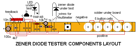
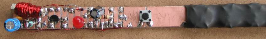
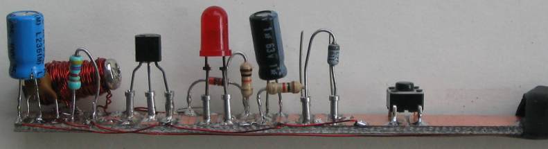
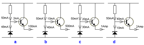
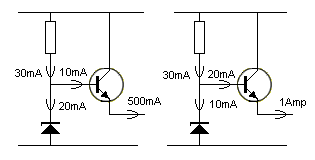

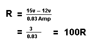
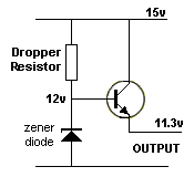
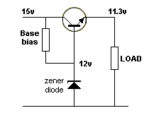
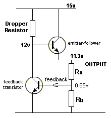
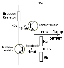
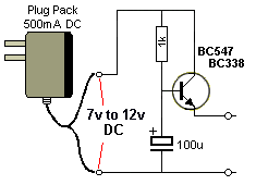
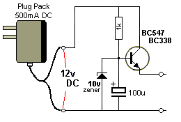
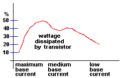
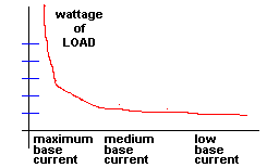
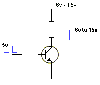
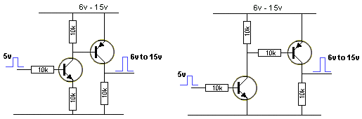
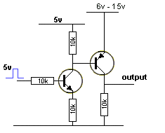
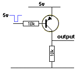
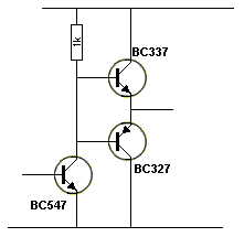
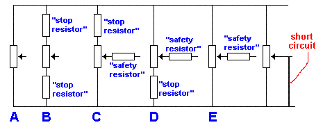
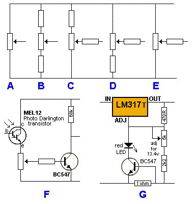

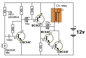
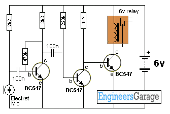
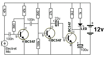
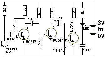
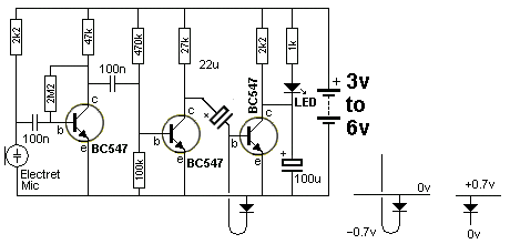
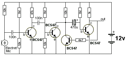
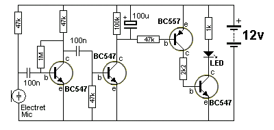
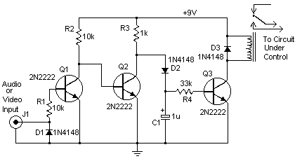
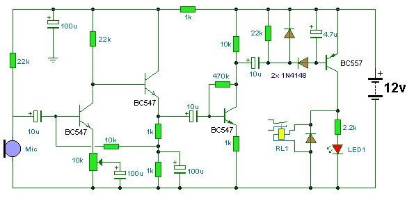
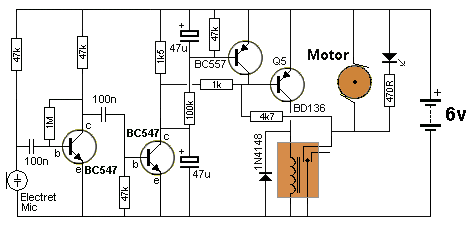
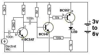
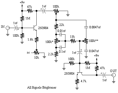
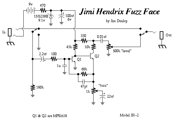
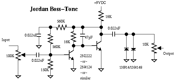
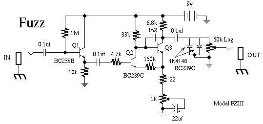
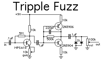
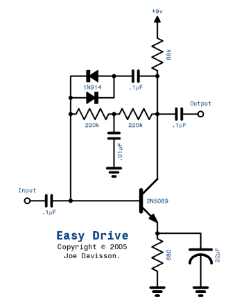
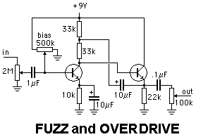
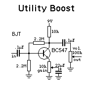
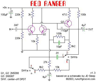
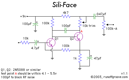
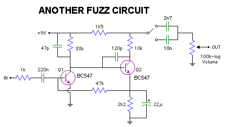
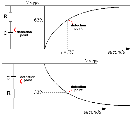
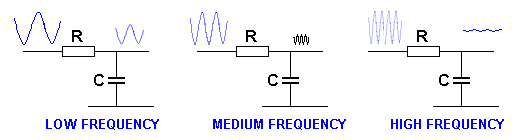
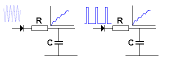
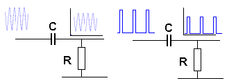
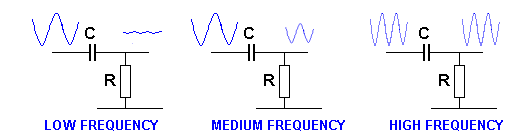
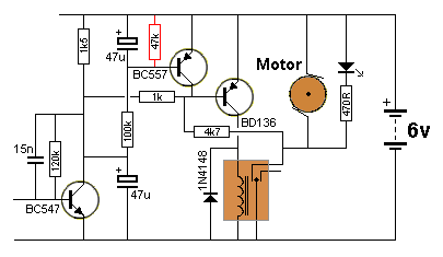

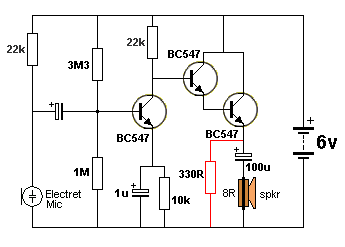
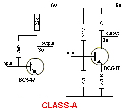
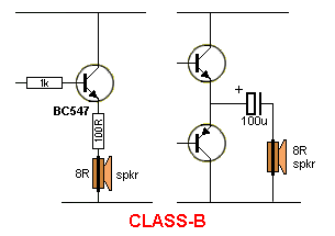
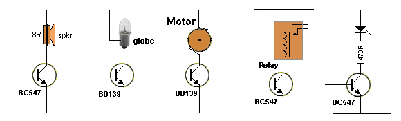
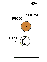
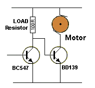
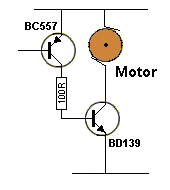
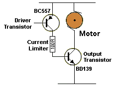
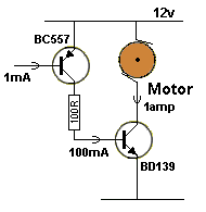
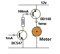
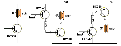
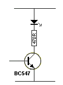
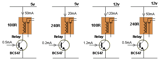
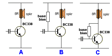
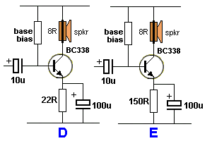
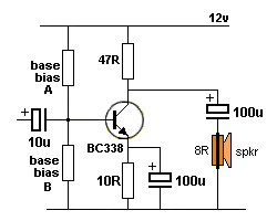
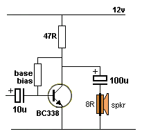
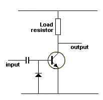
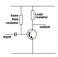
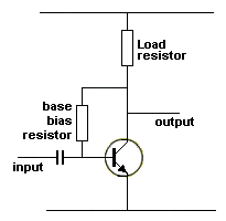
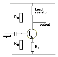
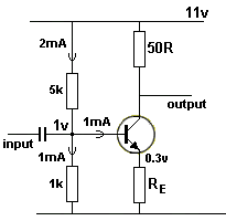
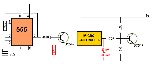
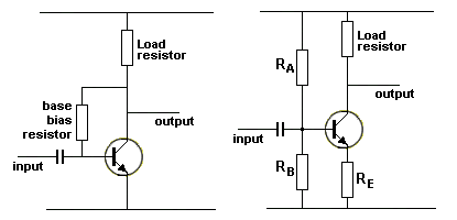
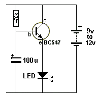
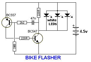
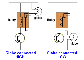
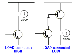
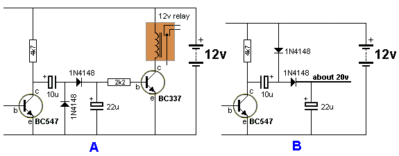
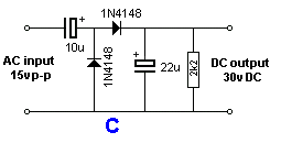
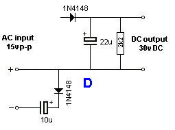
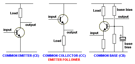
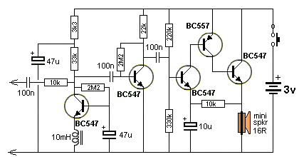
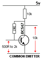
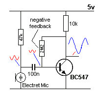
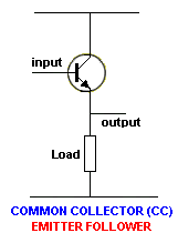
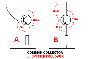
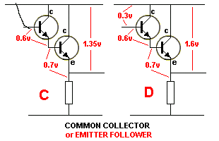
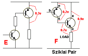
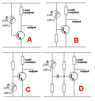
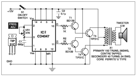
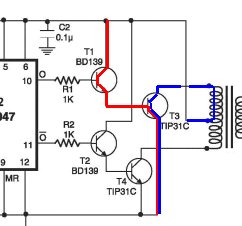
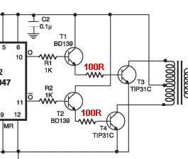
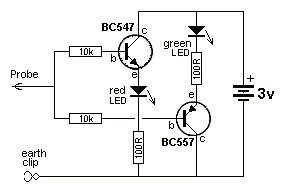
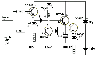
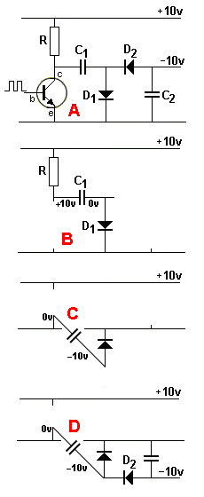
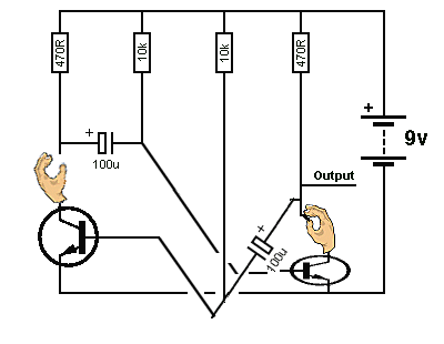
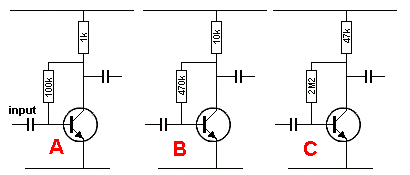
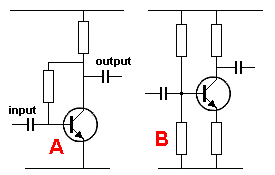
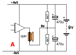
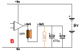
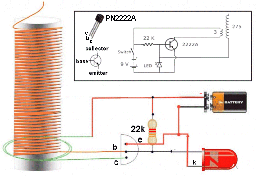
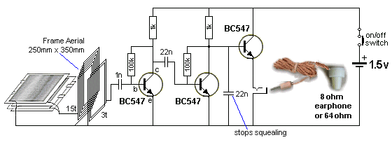
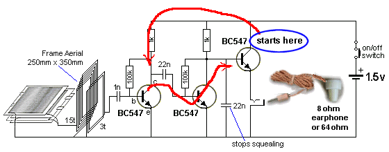
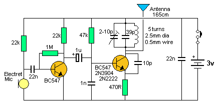
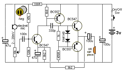
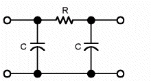
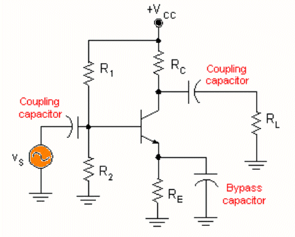

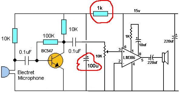
 In
the diagram, the zener is a 25v zener and the
transistor is rated at 25v between the collector-emitter
terminals. It is classified as a "25v transistor."
In
the diagram, the zener is a 25v zener and the
transistor is rated at 25v between the collector-emitter
terminals. It is classified as a "25v transistor."
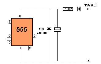
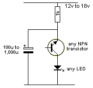 A
transistor can be placed in a circuit "around the wrong way" and
the a junction inside the transistor will breakdown at a fairly
low voltage.
A
transistor can be placed in a circuit "around the wrong way" and
the a junction inside the transistor will breakdown at a fairly
low voltage.  Here is a circuit using the breakdown of a transistor to produce
a frequency to drive the BOOST circuit.
Here is a circuit using the breakdown of a transistor to produce
a frequency to drive the BOOST circuit. 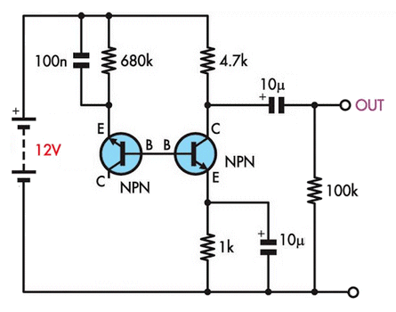 The
base-emitter junction can also be used but the voltage at which
the junction "breaks-down" and the voltage at which it does not
conduct is very small.
The
base-emitter junction can also be used but the voltage at which
the junction "breaks-down" and the voltage at which it does not
conduct is very small. 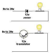
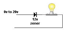
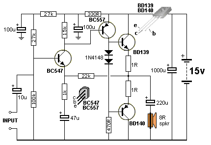
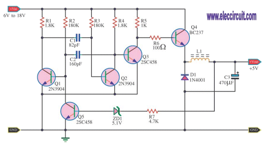
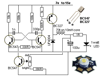
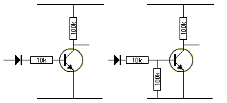
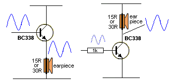
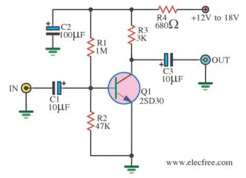
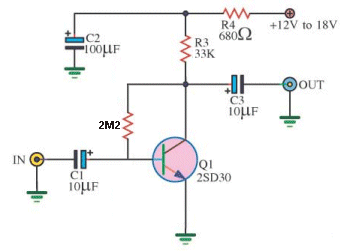
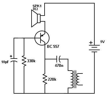
 This circuit above is poorly designed and has a
number of fundamental faults.
This circuit above is poorly designed and has a
number of fundamental faults.