SPOT
THE MISTAKES!
Page 12
![]()
We start another page of faults, hints and corrections to circuits found
on the internet.
I am surprised at the number of faults and poor designs produced by authors
who boast a university degree and experience in prestige places such as
NASA’s Jet Propulsion Laboratory, as stated by our first designer: Chris @
PyroElectro.com
His circuit for a White Line Following Tank has a number of points
worth mentioning. Here is his circuit:

The layout is a "dogs breakfast."
The first thing that "threw me" was the diode on the TIP120 transistor. I
could not see what is was doing.
Then I had to work out that the TIP was a Darlington transistor.
There were other mistakes but the layout was so poor I had to redraw the
circuit to make it easy to understand. The result is shown below:

The circuit is over-designed.
This is easy to see.
The TIP120 is pulled HIGH via a 330R resistor.
A photo-transistor receiving light has a resistance of about 300R. This
means only a single amplifying stage is needed between the photo-transistor
and the Darlington output transistor.
In addition, the base of the transistor driving the second motor could be
taken from the collector of the first TIP120 transistor.
This would save 2 transistors.
Two diodes and a resistor have removed from the original circuit as they are
not needed.
The circuit does work, as shown in the following photo and a full
description of its construction can be found at:
http://www.pyroelectro.com
and an eBook on building Robots:
http://www.pyroelectro.com/book/Building-Robotics-&-Electronics.pdf
The only point I am making is the fact that the circuit had no component
values ( I added the values from the construction-notes), the layout was
incomprehensible and is over-designed.
The author was informed of these details and has failed to
update the circuit.
I realise many authors are extremely embarrassed when confronted with faults
and most completely fail to respond.
That's why it is so dangerous to surf the net and conclude that everything
you see is correct and functional.
Before accepting any circuit, collect at least 2 or 3 similar designs and
see if they correspond with each other.

![]()
This circuit is a good design but the 10k resistor (R3) is not needed and the 5v1 zener diode serves no purpose. The output voltage is being determined by voltage across the collector-emitter terminals of Q2 (about 5v) and the zener voltage. Why not simply use the voltage divider consisting of R3 VR1 and R4 to create about 10v across the collector-emitter of Q2 and remove the zener. The circuit will operate exactly as the original design. With these changes we have eliminated two unnecessary components.

![]()
Here is a dangerous circuit from Alternative Energy Circuits Blog by

If both pots are turned to low resistance, they will create a short-circuit
and will be damaged. A damaged lower pot will cause the output voltage to
rise and damage the circuit you are supplying.
Here is a another circuit from
Alternative Energy Circuits Blog by
The output voltage will not be 15.2v
Here is a another circuit from
Alternative Energy Circuits Blog by
The output is NOT 1.2v higher than the voltage of the zener diode.
The following circuit will activate the piezo buzzer when a 12v supply drops
to 10v:
The two transistors operate as a
Schmitt
Trigger.
Here's another
faulty design by
D.Mohan Kumar Here is his original article. The corrections
are in bold RED. The circuit is a terrible design but here is the best that can
be done with circuit: Transformer X1, diodes D1, D2 and capacitor C1
forms the charger section. X1 is the centre tapped 9-0-9 step-down
transformer with 500 mA current. Diodes D1 and D2 are rectifiers to convert 9
volt AC to 9 volt DC.
The answer by
2 pots are fine in the circuit. If the 2 pots are set to near
short condition - one will blow out like a fuse.
What an absurd statement to make.
It's designers like ![]()

The peak voltage produced by 24v AC secondary will be 34v. The transistor
will only pass the positive portion of the waveform to produce pulsed DC on
the output. The 47R and 170R voltage dividers will deliver a peak of 34/217
x 170 = 26v
Any battery connected to the output will see pulses of 26v and the charging
will never cease.
I don't see any purpose in this design and it is certainly not a "Regulated
Battery Charger" as stipulated on the website.
The only thing that may reduce the charging current is the limitation of the
transformer. It will possibly be a low wattage design.
The 47R needs only 0.5 watt.
It's absurd to use a high voltage secondary transformer then dissipate a lot
of wattage in the external components.
The circuit is a very poor design and shows how NOT to design a battery
charger.
![]()

![]()
Alternative Energy Circuits Blog is to say I am "nitpicking."
He claims everyone is clever enough to realise the circuits he has presented
on his site contain faults and no-one will fall into the trap of putting two
pots across the power rails and create a short-circuit, or build a battery
charger without knowing the characteristics of the transformer.
In addition, he claims it is quite normal to use a 1M pot to create a
resistance between 1k and 100R then measure the pot and substitute a
resistor.
He obviously has absolutely no idea of the capabilities of the average
reader on the web.
90% of readers are beginners and have no ability to correct a faulty design.
Neither
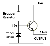
![]() A PNP transistor BC 557 functions as
a voltage controlled switch. As you know, PNP transistors forward bias and
conduct only when its base is grounded. A Zener diode is used to control the
switching of T1. In the 12 volt battery monitor, 10 volt Zener is used. When
the battery voltage is above 10 volts (The breakdown voltage of Zener), the
Zener conducts and the Base of T1 becomes positive and it remains off.
Buzzer will be also in the off state. Variable resistor VR adjusts the exact
biasing of T1 at 10 volts and C2 buffers the base of T1 positive as long as
Zener is conducting.
A PNP transistor BC 557 functions as
a voltage controlled switch. As you know, PNP transistors forward bias and
conduct only when its base is grounded. A Zener diode is used to control the
switching of T1. In the 12 volt battery monitor, 10 volt Zener is used. When
the battery voltage is above 10 volts (The breakdown voltage of Zener), the
Zener conducts and the Base of T1 becomes positive and it remains off.
Buzzer will be also in the off state. Variable resistor VR adjusts the exact
biasing of T1 at 10 volts and C2 buffers the base of T1 positive as long as
Zener is conducting.
Here is his mistake:
D. Mohan Kumar thinks the zener diode will break down at 10v and only a very
small voltage will appear across it. This is not so. At 10v, the zener will
break down and 10v will appear across it. However the zener is
connected between the emitter and collector of the PNP transistors and the
voltage between these two leads cannot be higher than 0.7v as this is the
characteristic of a transistor. So, the zener never sees 10v.
Here is the way to analyse the circuit:
As the supply increases from 0v, the transistor is turned on via the 4k7,
when the supply reaches about 0.8v. And as the supply increases, the current
through the emitter-collector leads increases. The supply can increase to
10v, 11v, 12v, 15v and the zener never sees more than 0.7v across its
terminals.


![]()


![]()

Diodes D3, D4 and the battery form the backup section. When the mains power is available, D3 forward bias to provide power to the battery and the load. When the mains power fails, D3 reverse biases and D4 forward biases so that current flows from the battery to the load. D3 prevents the back flow of battery current to the transformer.
Diodes D1 and D2 prevent reverse current to the transformer. D3 simply prevents the LED illuminating when the power fails.Resistors R3, R4, zener diode ZD and transistor T1 are the components of the cutoff section. When the battery voltage is more than 5.3 volts (4.7+0.7=5.4) zener conducts, taking the base voltage of T1 to ground.
No. The base of T1 sits at 4.7v Since T1 is a PNP transistor, the negative base bias allows it to conduct so as to provide load current. This is false. When the battery voltage drops below 5.3 volts, zener stops conducting and the base of T1 becomes positive through R3, R4 and it switches off. This is false. This cuts off power to the load. This condition remains as such till the mains power regains. This is ALL falseYou can see how many mistakes the author has made.
He has the wrong concept of how a zener diode works and no idea how to design a transistor output stage.
When the main is alive, the output current will be determined by the current though R4.
The current though R4 is 12v. - 0.7 - 4.7 = 7.2 divided by 10,000 = 0.72mA If the gain of the transistor is 100, the current will be 72mA.
The authors circuit simply does not work at all when the main fails.
The emitter sits at 6.3v - 0.7v = 5.6v and the base sits at 4.7v. This give a turn-on voltage of 0.9v. The battery only has to drop 0.2v and the circuit stops working. The output current will be a maximum of a few milliamps.
You cannot provide all the features the author is requiring when using a 6v battery. The diode- drops and transistor voltage-drops leave almost no voltage for the devices you are powering.
![]()
Here's another
faulty design by
D.Mohan Kumar
Here is his original article. The corrections
are in bold RED. The circuit is a terrible design as it uses a 12v lighter
battery to flash a 3v LED. A lighter battery has very little energy (about
23mAhr - 30mAhr) and is expensive. The circuit will not last very very long.
Here is a Dummy LED flasher to confuse intruders. It simulates the LED blinking of a sophisticated alarm system. It can flash for years both day and night using a single 12 volt alkaline battery (lighter battery).
The battery will last just a few days! If the life of the battery permits, it can flash continuously for more than 10 years. Theoretically it is true since the LED consumes less than 5 microamps. This is untrue. The LED consumes about 20mA. The interesting feature of the Flasher is that, the LED lights by taking current not from the battery, but from the capacitor. True.

The Circuit is simple and can be made match box size. It can
fixed to a door, window or car using double sided adhesive tape. The CD
4093 is a Quad NAND gate with 4 identical
Schmitt Trigger gates. Each gate has two inputs and one output. When
both inputs are HIGH, the output goes LOW.
Only one gate is needed for this project. The two inputs are connected together and the output is connected to R2 and the LED. Capacitor C1 charges through resistor R2. Since R2 is a high value, the charging current will be low (around 50 microamps). During this time, LED will be off. When C1 charges to 66% of the supply, the gate changes state and the output goes LOW. The stored energy in the capacitor lights the LED. The flash rate depends on the value of R2 and the brightness depends on the value of C1. If a high bright red transparent LED is used, the flashes are visible even in day light. Resistor R1 reduces the current to the circuit to prevent current loss from the battery. This is untrue. The unused inputs are tied HIGH and the chip gets its charging current via the inputs. You can remove the supply to pin 14 and the chip works exactly the same. This is normally NEVER done.
It is important to note that all the inputs and outputs of the unused gates should be connected to the positive rail to prevent floating.
This is entirely UNTRUE. You must NEVER connect the outputs to either rail - only the inputs to the POSITIVE RAIL
The circuit above is very poorly drawn. You cannot work out what the chip is
doing.
The following circuit has an improved layout:

The original circuit has been copied from the following circuit:

The circuit above can be simplified as the 1N4148 diode is not needed. It is
designed to prevent discharging the electrolytic when the gate changes
state, but the flash rate is very brief and the 330k will have no effect on
discharging the capacitor.
The 470R is not needed as we want all the energy from the electrolytic to
drive the LED.
![]()
Another faulty design by
D.Mohan Kumar The main fault is the circuit takes 10mA via the 555
when sitting around doing nothing.

A better design uses transistors and the circuit takes less than 20uA.

The LED will be illuminated for about 15 seconds via the clap of the hands.
The quiescent current is about 20uA, allowing 4 AA cells to last a
long time.
The circuit takes about 20 seconds to reset after the LED goes out. The
100u discharges through the 27k, 100k and 10k resistors.
![]()
Another faulty design by D.Mohan Kumar The main faults are the lack of a "Stop Resistor" on the Photo Darlington transistor and the wrong symbol for the transistor.


The circuit can be set-up on one side of a doorway to detect persons entering or leaving a premises. The other side of the doorway should have a mirror to reflect the beam. The piezo buzzer is an active device with a transistor drive-circuit enclosed in the unit. It produces a tone when a voltage is applied.
![]()
Another design by
D.Mohan Kumar The main fault is the unusual layout. Every type of
circuit has a prescribed way to lay it out. This allows you to instantly
recognise the type of circuit.
He is his layout:

Here is his terrible description of how the circuit works. Remember, he is a
University Professor in India with 20 year's teaching experience and has
presented over 200 circuits to all sorts of magazines in India. His
description is completely flawed and meaningless. It is the worst
description I have ever seen. It teaches nothing and leaves out the
important functions of how the circuit changes state. It is no-wonder Indian
students have no understanding of how circuits work. The teachers themselves
are confused.
It is very difficult to see what the circuit is doing, when it is drawn
incorrectly.
Here's how the circuit works:
Here is a simple Dancing LED
circuit. The LEDs turn on/off alternately giving a dancing appearance. It is
a simple astable multivibrator using two NPN transistors. It works on a
principle of charging and discharging capacitors C1 and C2. Current from the
positive of the battery flows through the first set of LEDs D1 - D3 to the
collector of T1 through resistor R1. Resistor R1 limits current through the
LEDs to protect them. The current through R1 charges capacitor C2. It then
discharges through the base of T2 and resistor R4. This gives base current
to T2 and it conducts. As a result, the second set of LEDs D4 - D6 light as
the current flows through T1. Capacitor C2 again charges and the cycle
repeats.
The same thing happen on the other side. This gives alternate flashing of
the LEDs.
This description is utter rubbish.
No-where does he mention the charging of C1.
All circuits need to be drawn correctly so it is easy to see what it is
doing.
When it is drawn correctly, you can see it is an astable (non-stable - free
running) multivibrator.

When the power is applied, both transistors have 47k resistors connected to
the bases and both will start to come on. But one transistor will
come on slightly faster than the other. This is called "racing" and the
transistor that comes on slightly faster will pull the positive lead of the
uncharged 10u towards the negative rail and this will reduce the turn-on
voltage to the other transistor.
We now have the case where the left transistor is tuned ON via the second
47k and the left three LEDs are illuminated.
How, here the part that no-one has mentioned before.
The first transistor is also turned on by the second 10u charging via the
three LEDs and 100R. This add to the turn-on of the transistor and adds to
its "saturation" In other words it is tuned on more than just the effect of
the 47k resistor.
This causes the collector-emitter voltage to be very low.
During this time the first 10u electrolytic is also charging (in reverse)
and the second transistor is starting to see base-emitter voltage.
The second 10u is getting nearly fully charged and the "charge-current"
starts to reduce.
This turns off the first transistor very slightly and the collector voltage
rises. The positive end of the 10u rises and takes the negative lead higher.
This action starts to turn on the second transistor and the collector
voltage falls. The positive lead of the second 10u falls and takes the
negative lead lower. This starts to turn off the first transistor and the
first 10u rises to turn on the second transistor. This is how the two
transistors change state.
We mentioned the first 10u was initially charged in the reverse direction by
about 0.5v as the positive end was 0.2v about the 0v rail and the negative
lead had about 0.7v on it.
When the first transistor turns off, the positive lead rises due to the
characteristic volt-drops of the three LEDs and it starts to charge with a
high current. This current firstly discharges the electro and starts to
charge it in the other direction. This fully saturates the second transistor
and makes the collector-emitter voltage very low.
As the charging current reduces the second transistor becomes less
tuned-on and the collector-emitter voltage rises. As we said above,
this is how the two transistors
change state.
This description is a far-cry from Professor Mohan Kumar's understanding of
the issue.
The operation of this type of circuit is much more complex than you think.
![]()
Here's
Another stupid design by
D.Mohan Kumar
Here is is his description. He has absolutely no concept of how to explain
the operation of the circuit.
A thin wire loop is used to keep the alarm off in standby mode. Preset VR1 is
used to adjust the voltage at pin 3 of IC1
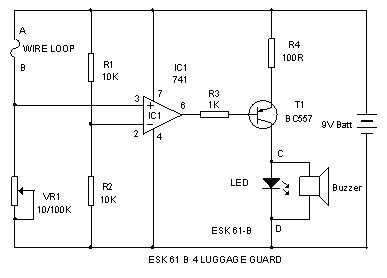
Normally current passes through the wire loop to pin 3 of IC1. So pin3 of IC1 gets more current than pin2.
(this is NOT TRUE) This makes the output of IC1 high. The high output from IC1 inhibits the transistor from conducting. So LED and buzzer remain off. When somebody takes the luggage, wire loop breaks and current to pin 3 drops (The inputs are voltage controlled - not current controlled). As a result voltage at pin 3 becomes zero and the output of IC1 becomes low. This allows T1 to conduct and buzzer sounds and LED lights. Tie the wire loop around the luggage so it breaks when the luggage is pulled.The circuit above is over-designed, and it has a major fault. If the 10k pot is turned fully, it will create a short-circuit with the wire loop. In addition, the circuit takes a high current when not doing anything. In addition, the buzzer will never work as it sees only 1.8v.
This circuit has never been tested and Professor D.Mohan Kumar should stop making a fool of himself by publishing such rubbish on his website. It's no wonder Indian students look to overseas to get an education.
Half of Talking Electronics 9GB of traffic each day comes from India. It is unbelievable how India is advancing in this technological age.
I get emails from Indian businessmen who was to make cheap LED lights for villagers who don't have electricity, so you can see the enormous range of social benefits in this country.
On the other hand I see Indian lecturers on videos trying to teach electronics. I can hardly understand what they are trying to present. It's no wonder students don't understand.
Now, back to the answer for this circuit:
All that is required is two transistors and three resistors, as shown in the circuit below:

![]()
Here's Another disaster by D.Mohan Kumar
He claims to test all his circuits. This is one of the poorest designs for an FM
transmitter. See our article Spy
Circuits for a full description of how to design this type of circuit.
Remember, this is a University Professor from India, describing the circuit. It
is the most inaccurate description I have come across and quite a useless design
as far as FM transmitters are concerned. .

Here is his wording for the details of each component.
The condenser MIC is used to pick up the sound signals. The diaphragm inside the MIC vibrates according to the air pressure changes and generates AC signals. (He does not mention anything about the FET transistor inside the case. He knows nothing about this type of microphone). Variable resistor VR1 adjusts the current through the MIC and thus determines the sensitivity of MIC. (If the 10k is turned fully it will completely damage the microphone. Very dangerous. A very poor design). The condenser MIC should be directly soldered on the PCB to get maximum sensitivity (rubbish) . Sleeving the MIC inside plastic tubing can increase its sensitivity enormously.
2. Decoupling Capacitors
C1 is the first decoupling capacitor (It is a coupling capacitor not a decoupling capacitor) impedes the different frequencies of speech signals. (not an accurate description). C1 modulates the current to the base of transistor. The 4.7 uF capacitor isolates the microphone from the base voltage of the transistor and only allows alternating current (AC) signals to pass.
A large value capacitor induces bass (low frequencies) while a low value one gives treble (high frequencies). Capacitor C2 (0.01) act as the decoupling capacitor (not really. It actually couples the base to the rail). Capacitor C3 across the transistor T1 keeps the tank circuit vibrating. As long as the current exists across the inductor coil L1 and the trimmer capacitor, the tank circuit (coil-trimmer) will vibrate (oscillate) at the resonant frequency. When the tank circuit vibrates for long time, the frequency decays due to heating (the losses are due to magnetic losses and losses in charging and discharging the capacitor). Presence of the capacitor C3 prevents this decay. A capacitor between 4 and 10 pF is necessary. (Poorly presented and reasonably inaccurate - he has not told you anything).
3. Resistors
Variable resistor VR1 restricts the current through the MIC. The voltage divider R1 and R2 limits the base current of T1 (not really - it puts 3v on the base) and R3 forms the emitter current limiter. The given values are necessary for the 2N 2222A transistor. (He has not mentioned the transistor is a common-base stage).
4. Transistor
2N 2222A is the common NPN transmitter used in general purpose amplifications. It has maximum power rating of 0.5 Watts. Over-powering of 2N 2222A can generate heat and destroy the device. So maximum power output should be around 125 milli watt. (the output of this circuit is about 30mW)
5. Inductor Coil
The inductor used in the circuit is a hand-made coil using 22 SWG (Standard Wire Gauge) enameled copper wire. The length, inner diameter, number of turns etc are the important values to be considered while making the inductor. Then only the inductor resonates in the 88-108 band FM frequency. (badly worded). For this circuit, the coil radius was selected as 0.26 inches (outer diameter) and 0.13 inner diameter. Coil can be wound around a screw driver (with same diameter) to get a 5 turn coil of 0.2 inch long. Remove the coil from the screw driver and use the 5 turn air core coil. Remove the enamel from the ends and solder close to the transistor.
6. Trimmer capacitor
A small variable capacitor with a value of 5 -22 pF can be used to adjust the resonant frequency of the tank circuit. The variable capacitor and the inductor coil form the tank circuit (LC circuit) that resonates in the 88-108 MHz. In the tank circuit, the capacitor stores electrical energy between its plates while the inductor stores magnetic energy induced by the windings of the coil.
Tank Circuit
Every FM transmitter needs an oscillator to generate the radio Frequency (RF) carrier waves. The name 'tank' circuit comes from the ability of the LC circuit to store energy for oscillations. The purely reactive elements, the C and the L simply store energy to be returned to the system (badly worded). In the tank (LC) circuit, the 2N 2222 A transistor and the feedback 4.7 pF capacitor are the oscillating components (badly worded). The feedback signal makes the base-emitter current of the transistor vary at the resonant frequency (badly worded). This causes the emitter-collector current to vary at the same frequency. This signal is fed to the aerial and radiated as radio waves.
FAULTS
Apart from the 10k pot damaging the electret mic, the circuit needs a 22n across the battery. This improves the output considerably.
The 10k and 4k7 voltage-divider resistors put 3v on the base and the transistor operates in the range of about 3v. Using a 9v supply is a complete waste of voltage. The circuit will work with a 3v battery and a single 47k base resistor.
The 4u7 can be 100n with no difference in quality.
The 100R emitter resistor is too low. It should be 470R.
Overall a terrible copy of a single transistor FM transmitter that can be found on the web with fewer mistakes than is design.
See our article Spy Circuits for better FM transmitters.
Here's another disaster from Professor D.Mohan Kumar who knows nothing about electronics' design:
20 kHz IR Transmitter
This continuous tone IR transmitter can be used in Broken Beam Detector
system to activate an alarm. The circuit is a simple multivibrator and an IR LED
driver output. This transmitter is useful in Photodiode and Phototransistor
based IR receivers.
![]()
Faulty 20kHz transmitter - do not
construct!
IC1 is designed as a simple oscillator using the
components R1, R2 and C1. With these components, output pulses will be around
20kHz. The effective range of the IR beam depends on the peak current to the IR
LED rather than the mean current. Around 100-200mA current is necessary to
increase the transmitting range. Hence the output pulses from IC1 are fed to a
LED driver circuit comprising T1 and T2. When output of IC1 is high, T1 is
driven into saturation via R5 and red LED turns on. When T1 conducts, T2 turns
on to drive the IR LEDs. When the red LED turns on about 1.8 volts develop
across the LED and around 1.2 volts develop across R6
(10.2v develops across the 100R resistor - this is the BIG MISTAKE!).
Thus T2 acts as a constant current generator (NO
. ... IT DOES NOT) and with R6, the peak current flowing through IR
LEDs is around 170 - 200mA (1.2 / 6.8 =0 .176 A or 176 mA)
(The calculations are WRONG!!!! The current though the IR LEDs
will be more than one AMP!!!! They will be DAMAGED!!! )
When the output of IC1 goes low, T1 and T2 turns off and IR LEDs switch off.
IC1 is the CMOS low power version of 555 IC. It works on 5 -15 volts DC.
More faults:
1. The circuit may not turn off as the 7555 goes low but not below 0.6v.
2. What is the function of the 22k. It should be on the base of the BC547
transistor.
3. C2 is not needed.
4. 6R8 is too low. It will instantly damage the IR LEDs.
5. Both transistors will be instantly damaged when the circuit turns ON. The
current will be about 1.5 amps!! - through the 6R8
and emitter-base of the BC557 and collector-emitter of the BC547.
I have contacted Professor
D.Mohan Kumar more than 10 times with all his previous faulty
circuits, and yet he continues to pump out this RUBBISH on his web pages.
He never tests anything and I don't know why he fails to respond to any of my
corrections.
He is just an embarrassment to the electronics industry and it is fortunate we
don't have many fools like this in the teaching profession. He is possibly
the WORST designer I have come across.
At least he provides a platform for the rest of us to study and learn.
Remember - don't make a fool of yourself. Test everything before you
release it.
I have things sitting on the bench at the moment - turning ON and turning OFF to
the sounds of the TV - just to prove a circuit works over a long period of time
and remains working when the battery voltage reduces.
![]()
Here's another circuit from:
http://www.circuitstoday.com/
Never connect two transistors so that current can
flow from the positive rail to the 0v rail via the junctions of the
transistors. If you supply sufficient current into the base of the first
transistor, a larger current will flow via the collector emitter leads of Q1 and
this current will flow from the emitter to base junction of Q2.
The answer is to add a resistor called a SAFETY RESISTOR as shown in the
following diagram. The resistor will not alter the performance of the circuit
but it will limit the maximum current:
Here's a circuit from CIRCUIT DIAGRAM.ORG The website is owned by:
Salman Feroz Ali
Here is his description of the circuit:
The diagram is a fully automatic NiMH battery
charger circuit using a 7805 voltage regulator which is providing a constant current to charge
2 NiMH cells. The LED works as a charging indicator so when the cells become fully
charged the LED will go off. The circuit can charge two NiMH cells at a time. The circuit has four different current sources: 50mA,
100mA, 150mA and 200mA which is selectable with the switch S, so you can choose
the current source for your cells. For example if you want to charge
500mA NiMH rechargeable cells you have to select 50mA current, for 1000mAh NiMH
cells select 100mA, for 1500mAh select 150mA and to charge 2000mAh
cells select 200mA.
1. The symbol for a microphone is a carbon microphone. These are no longer
available. The symbol should be an electret microphone.
The circuit works on the basis of a
high-gain amplifier being driven into saturation (fully turned-on), firstly by
the very small amount of current delivered by the 2M and then from energy stored
in an electrolytic.
Mistakes in the circuit:
The charging current is about 20-30mA. It will take about 7 days to charge the
battery and this will allow illumination for 5 hours, once per week.
He writes:
1. The 3v1 zener is connected across the battery !!!
The first stage is badly designed.
This is the most dangerous power supply I have ever seen.
The peak voltage of a 230v AC supply is about 320v. Two equal capacitors
will produce a voltage equal to half the peak value, at their join, as shown
in the following diagram:
This means the capacitor-fed power supply will always be 160v higher than
the neutral - no matter which way the power supply is connected.
Page 1
Page 2
Page 3
Page 4
Page 5
Page 6
Page 7
Page 8
Page 9
This current can overheat and damage the transistors.


![]()
from Karachi Pakistan
http://circuitdiagram.org/automatic-nimh-battery-charger-circuit.html
The only problem is the LED will never illuminate. The second transistor is
always ON. The circuit cannot detect the exact voltage when the two cells are
charged. Since the charging current is about 1/10th the rating of the cells, it
will take about 14 hours to fully charge flat cells.
![]()

![]()
![]()
2.Turning the 10k pot fully will destroy the microphone. It should have a 1k
"stop resistor."
3.The 1k connected to the 470n does nothing.
4. The coil should be 5 turns on 3mm former. The energy from the coil should
match the energy from the capacitor.
5. The 62p does nothing.
6. The 3p on the antenna simply reduces the range.
![]()
![]()
![]()

![]()


![]()


When the energy from the electrolytic has been fully delivered, it cannot keep
the amplifier fully turned on and it turns off slightly. This action removes
the "turn-on" effect from the electrolytic and the amplifier begins to turn off.
This action continues until the amplifier is fully turned off and is kept in the
off state while the electrolytic begins to charge. The off-state is very long
and the on-state is very short. This is how the LED produces a brief flash.
Here is the technical description of the
operation of the circuit:
When the supply is connected, both transistors are off and the 2u2 electrolytic
charges via the 2M2 resistor and 68R. When the voltage on the base of the first
transistor rises to about .6v, it begins to turn on and the resistance between
its collector-emitter terminals is reduced. This allows current to flow in the
collector-emitter circuit of the second transistor via the 1k resistor. The
second transistor conducts and the LED is illuminated. The current through the
LED is limited by the 68R resistor and at this point in the cycle a voltage is
developed across the 68R. The negative end of the electrolytic is "jacked up" by
this voltage and the positive end pushes the charge on the electrolytic into the
base of the first transistor to turn it on even harder. In a very short time all
the energy in the electrolytic has been delivered and it cannot hold it ON any
longer. The transistor turns off slightly and this has the effect of turning off
the second transistor a small amount. The LED begins to turn off and the voltage
across the 68R reduces. The negative lead of the electro drops a small amount
and so does the positive lead. This action continues until the first transistor
is fully turned off. This turns off the second transistor and the LED is
extinguished. The cycle starts again by the 2u2 charging. The charge-time is
considerably longer than the discharge time and this gives the LED a very brief
flash.
Why doesn't the original circuit work?
The 50u is connected to the top of the LED. When the two transistors
start to turn off, the negative end of the electrolytic has to be pulled to the
0v rail and this will pull the positive lead down too. The "pulling-down" effect
has to be greater than the charging provided by the 2M2 so the two transistors
get fully turned off.
In the original circuit, the LED can only pull the right lead down to 1.7v and
this allows a turn-on voltage to exist on the base of the first transistor. The
transistor remains ON and the LED remains illuminated. Two more points to note:
The 2M2 must be a high value otherwise the circuit will not turn off as it will
start to charge the electrolytic during the time when it is being "pulled-down."
The 68R cannot be higher than 100R otherwise the circuit will not turn off as
the current through this resistor this resistor must be a considerable amount so
that the PNP transistor needs a fairly high base current . When the transistor
does not get this current, the circuit is able to turn off.
![]()

When the power fails, the transistor will never turn ON. D5 will not pull the
base of the transistor to 0v rail. The transistor will just be left
"floating."
Resistor R1 restricts the charging current to 10mA. It should be 10R. The
100R resistors to the 1 watt LEDs will only allow allow 30mA, or 100mW to the 1w
LEDs. R3 and R4 should be 10R 1 watt.
The value of resistor R2 is too high. It will never allow the transistor to pass
600mA.
This circuit has never been tested.
The following circuit is the simplest design needed.

A charging current more than 50mA will gradually "dry-out" the battery and
shorten its life.
If the project is used more than 5 hours per week, the charging current can be
increased.
The 220R charging resistor can be reduced to 150R or 100R.
![]()

This circuit protects home appliances from low voltage. When the voltage in the
AC lines drop below the normal voltage, the circuit cuts off power to the
appliance and keeps it off till the normal voltage resumes. It is useful to
protect appliances like fridges which may over heat if the line voltage drops
below 180 volts. Low voltage increases the current consumption in a fridge due
to over-stressing the compressor.
The circuit uses a zener controlled relay driver to switch the load. A 9v 500mA
transformer provides power for the circuit. Any voltage drop in the primary of
the transformer reflects as a corresponding voltage drop in the secondary. So
when the line voltage is normal (around 230 volts), the zener conducts to bias
the relay driver transistor T1.When T1 conducts (as indicated by the glowing
LED), the relay is energized and switches the load ON. The load is connected
through the Common and Normally Open (NO) contacts of the relay.
When the mains voltage drops below 200 volts, a corresponding voltage drop
occurs in the secondary of the transformer and the zener turns off. T1 then
turns off to de-energize the relay. The load remains off till the line voltage
increases to normal.
Capacitor C1 gives a short lag before the zener switches to avoid false
triggering of T1 if the line voltage fluctuates.
It is necessary to adjust the trigger point using the preset VR. Check the line
voltage and if it is above 200 volts, slowly adjust the wiper until the LED
turns on and the relay energizes.
Three faults/improvements are:
1. The zener diode is not needed.
2. R2 is not needed.
3. C3 is not needed.
![]()

![]()

The electret mic should not be connected to the base without a load resistor.
Pin 2 of the 555 should have a 1M resistor to the positive rail to prevent false
triggering.
Pin 2 is high impedance and it is not capable of charging or discharging the
100n.
![]()
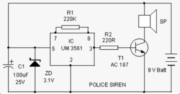
2. Where can you get a 3v1 zener????
3. Where can you get AC187 ? They have not been manufactured for 15
years!!
4. They cost $5.00 each !!!!!! Plus postage
5. What is the impedance of the speaker?
This is another untried circuit from
![]()

A piezo element is called a HIGH IMPEDANCE DEVICE. It can produce a voltage when
it is hit or bumped but the current is very small.
The load resistance on the first stage is 1k. This is classified as a LOW VALUE.
A transistor merely amplifies the current it receives via the base and allows
about 100 times more current to flow in the collector-emitter circuit.
To produce a voltage-drop across the 1k resistor of 1v, 1mA must flow. The base
must receive 10uA. And the voltage from the piezo element must be greater
than 600mV.
A piezo element produces about 20mV to 50mV when it detects sound. A heavy
strike may produce a few hundred mV. But this circuit is very unreliable.
The author has then amplified the signal produced by the first stage.
Instead of making the first stage very insensitive, he could make it more
sensitive and this would require only one stage.
See "Knock Knock Doorbell"
for the correct way to design a piezo-detection stage.
The biasing components for the second stage are all incorrect.
The 10k pot is in the wrong place.
Sensitivity adjustment is normally placed as the collector load. It should be
100k.
The 4M7 is too high. It should be 1M.
Diode D1 is not needed. It serves NO purpose.
In fact it should not be used. It puts a high-impedance on the input of the IC
when at rest and this will allow noise to enter the chip.
It's just a badly-designed circuit.
This type of design shows a complete lack of understanding of electronics.
![]()

The two capacitors on the front end produce a voltage-divider. To see
what I mean, remove all the power supply components, including the bridge,
and connect the two 220n capacitors together as shown in the following
diagram: 

A normal capacitor-fed power supply has one side connected to the neutral
and the output is classified as "ground-referenced." This means the
capacitor power supply can be touched (although it is not recommended as the
input connections may be around the wrong way and the supply is really 340v
above "earth").
However the supply shown above is always "180v HOT" - no matter which way
the supply is connected.
It is totally isolated from mains supply using two
capacitors in the phase and neutral lines.
So the connected device is safe even if the phase and neutral lines changes.
We know how wrong he is!!!
![]()

![]()
Page 10
Page 11 . . .
Page 13