SPOT
THE MISTAKES!
Page 11
![]()
Here is a circuit that is over-designed:
It can be simplified to this:
Before designing a circuit, look on the web and
carry out research to see what has been done by other designers.
There are a number of
mistakes on the circuit. The main problem is the layout. It is not clear
what the transistor is doing.
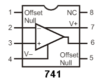
When the component values on the inverting and non-inverting inputs are included on the diagram, we
can see how the circuit works.
Here is another disaster from Electronics For You:
And the 1k on pin 5 is not needed. The diagram above shows the connection of
pin 5 to one of the comparators and three 5k resistors. Adding a 1k to the
10k pot on pin 5 is not going to have any affect at all. As I have said before, look at each
component and ask yourself: "Is this needed?" Adjusting the 555 frequency
via pin 5 is very unusual, normally the timing resistor between pins 6&7 is
adjusted, and two components could be removed.
Another circuit from Electronics For You:
Here is the simplified circuit:
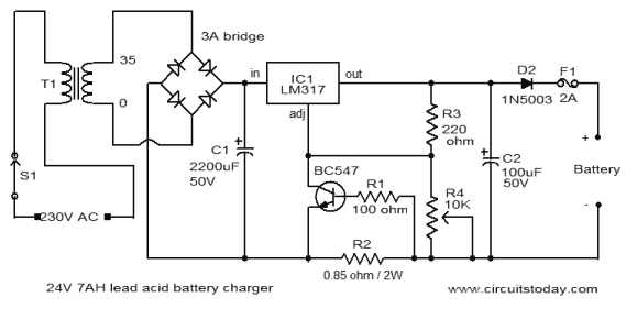
More from CircuitsToday.com:
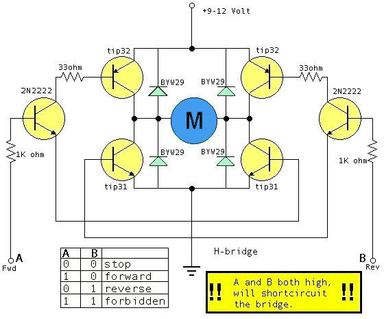
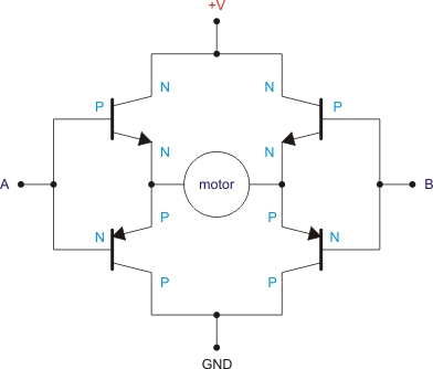
The next circuit shows how the 4 transistors in the bridge must be
cross-coupled so that diagonally-opposite transistors are activated to turn
the motor in either forward or reverse direction. But in the circuit below
BOTH inputs A and B must not be HIGH at the same time or the 4 transistors
in the bridge will be turned on and create a SHORT-CIRCUIT.
The following circuit creates a short-circuit across the power supply each
time the input changes from one state to the other. One reader created the
circuit with MOSFETS and they were constantly being destroyed in the
microsecond that the transfer took place from forward to reverse or reverse
to forward.
The following circuit is a disaster. When either the left or right section
is turned on, the voltage-drop across the junctions of the three transistors
is less than 2v. A very high current will flow via the base-emitter
junctions of the top and bottom transistors (and the collector-emitter of
the middle transistor) and they
will be destroyed:
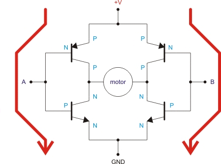
The following circuit shows a high current flowing through the PN junctions
of the transistors (follow the arrows on the transistors to see what we mean) and this type of
layout is to be avoided:
The following circuit shows the correct placement of the transistors to
prevent a SHORT CIRCUIT:
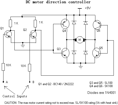
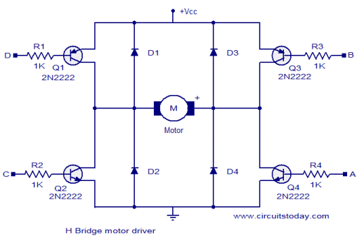
The following circuit shows 4 transistors in an H-Bridge. The designer says
the circuit will deliver 800mA but the 1k resistors on the base will not
saturate the 2N2222 transistor sufficiently to deliver this current. In
addition, a motor takes 2-5 times more current when starting and that's why
the transistors must be able to deliver a very high current.
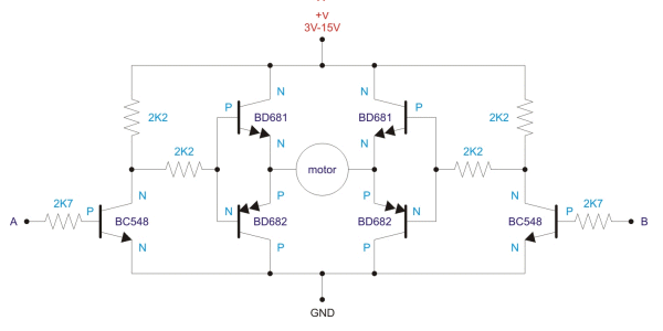
The following circuit solves the problems mentioned above and the control
voltage can be lower than the supply to the motor. To understand what we
mean you will have to look on the web for H-bridge designs. This article
only highlights faulty H-bridge circuits. The double arrow on the
transistors indicates a Darlington Transistor. The 2k2 resistors can be
reduced to 100R to increase the drive-current to the motor.
The following circuit will create a short-circuit across the power supply
when any of the inputs are active.
There is nothing really faulty with the following circuit except the fact
that the output of the bridge will be 35 x 1.4 = 50v plus about 7v (to allow
for voltage-drop due to a term called "regulation") making the output voltage
35v AC. This means about 25v will be dropped across the regulator and if the
max current is 800mA, the wattage lost in the regulator will be 20
watts. This makes the circuit about 50% efficient and the regulator will
need to be mounted on a large heatsink. The aim with all circuits similar to
this is to keep the input voltage as low as possible to reduce the heat
generated by the regulating components.
The circuit above is not a Wheatstone bridge as a bridge
must have 4 resistors and a change in any resistance will
deflect the needle either up-scale or down-scale.
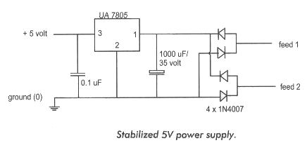
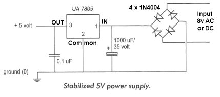
Here's a circuit from an electronics book. It doesn't have a fault but the
circuit is not instantly recognisable:
In the second circuit, the 4 diodes are easily recognised as a bridge and
the pins on the regulator are marked as IN Common OUT. The circuit does not
need 4 x 1,000v 1N4007 diodes.
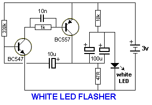
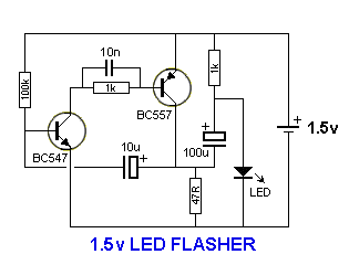
This is an example of over-design:
The same applies here. The upper circuit can be simplified to:
Circuit 2 takes less current and flashes the LED with a much
brighter illumination. You can use 220u for an even brighter flash.
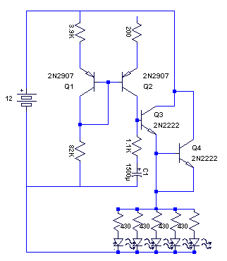
Here's another example of over-design. The following circuit was designed on
a simulation package and although it does work, it has about 5 components
that are not needed.
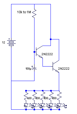
The following circuit is a copy of the one above with all the unused
components removed and Q4 correctly wired:
A simulation package does not make corrections to your design and you must go
through each component and ask: "Is this item necessary?"
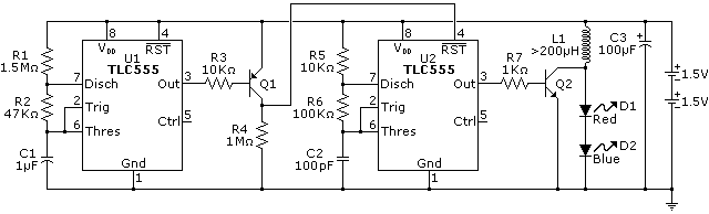
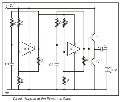
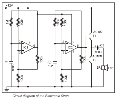
Yet another example of an over-designed circuit:
The circuit above can be simplified to one of the following:
The original circuit has a major draw-back. The 555 takes 10mA and
this is wasted current. The other two designs take much less than 1mA.
If you want a transistor circuit, here's a suitable design:
Before designing a circuit, do some research. Look on the web for equivalent
circuits and see how your ideas compare with other designs. You will be
amazed how much you can learn.
Here's a circuit that does not work. But you are not aware that some
components are missing because the IC is a "double-555:"
When the circuit is redrawn, you can see the electrolytic is not being
charged via the supply or discharged by the chip.
Here is a simpler circuit that works:
Apart from the first circuit producing a very weak output, it uses a lot of
components. The second circuit produces a very bright flash and although it
is not extremely efficient in current consumption, (the 47R is placed across
the supply during the short flash-period), it will work on a supply down to
2v.
![]()
Here's another circuit from Electronics For You, an Indian Magazine:![]()
We will rearrange the circuit and things will become clearer.
![]()
Here are the faults:
1. LEDs should not be connected across each other as each LED creates a
slightly different voltage across it when it is working - called the
"characteristic voltage". To put 21 LEDs in
parallel will give very poor results.
2. There is no such thing as a 4v battery. All wet cells are 2.1v and you
are connecting 4.2v directly across LEDs that require an exact 3.6v max for
white LEDs. At 4.2v they will be instantly damaged.
3. When the switch is "OFF" the output of the transformerless power supply
goes though the LEDs and through the collector-emitter of the transistor.
The transistor is not turned on but the output of the power supply will rise
to 315v if no load is on the output. As the voltage rises, the transistor
will zener at the maximum voltage it will withstand. This could be 25v, 45v,
65v
or even higher.
It will definitely zener AT SOME VOLTAGE and the LEDs will illuminate.
That means the circuit does not have an OFF position.
If the transistor zeners at 65v, the 220u 16v electrolytic will have nearly
70v across it and it will be damaged.
4. The transistor is placed in a position of being damaged.
5. The 1u capacitor on the input will allow 150mA and when this is divided
between 21 LEDs, each will get 7mA. But some will get more and some
will get none as they are in parallel (across each other).
6. There is no safety resistor on the input to prevent surges entering the
LEDs if the circuit is turned on when the supply is at a peak. The
instantaneous current though the 1u is MANY AMPS. It's exactly the same
current that is available from a fully-charged capacitor, when the leads are
shorted together. That's why they use capacitors for spot-welding, due to
the very high current they can provide.
This is a very badly designed circuit and the layout of the original circuit
makes it very difficult to see the faults. That's why it is so important to
layout a circuit correctly.
And it's critical to test a circuit before putting it in a magazine that has
over ONE MILLION READERS.
![]()
Here is a typical circuit without any component values. I am sick of
seeing circuit diagrams like this.
They are obviously produced by a non-engineer. To an electronics engineer, a
circuit diagram is a complete picture and it is actually more than a blur.
An engineer can see the circuit working when he knows the value of the
components.
The circuit uses AC187, AC188 transistors in the output. These are germanium
types and went out of production 20 years ago. This circuit was presented in
an Indian magazine. The output will draw nearly 1amp but the transistors are
only designed for 300mA. You can trust the Indians to get things wrong.
The principle of an op-amp is to provide a very high gain. This means a
small change in either input produces an almost full rail swing on the
output.
The circuit starts to work like this.
As soon as you put a slight voltage on the "+" input, the output goes full
HIGH.
The two 100k resistors on the "+" makes the output go full HIGH.
Now we connect a resistor from the output to "+" and this makes no
difference. The output remains full HIGH.
Now we put a resistor from output to "-."
If the "-" input is slightly higher than "+" the output goes LOW. This is
what happens. The output voltage drops until the "-" input is slightly lower
than the "+" input and that's why the output falls until its voltage is
equal to the "+" input.
Now we connect a capacitor to the "-" input.
It does not matter if we add the capacitor later or turn the circuit on with
the capacitor fitted.
The voltage on the "-" input will be lower than the "+" input and this will
start the circuit oscillating.
This is how it oscillates:
Because the "-" input is lower than the "+" input, the output rises towards
the positive rail and this begins to charge the capacitor.
The voltage on the "-" input can rise higher than the "+" input and when it
is about 15mV higher, the output drops towards the 0v rail.
This reduces the voltage on the "+"input and the capacitor has to discharge
a considerable amount before it is lower than the "+" rail. (Actually before
the "+" input is higher than the "-" input).
The voltage on the "+" input is rising and falling by about 30% of rail
voltage and this is the amount the capacitor has to charge and discharge for
the circuit to work.
But it is only when the component values and "+" and "-" are included on the
circuit that you can see how it works.
![]()
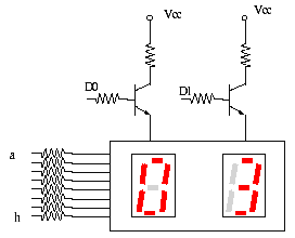
This design has mistakes. The resistor in the collector and the resistor in
the bases are not needed.
Firstly the resistor in the collector. When one segment is illuminated, a
small voltage will develop across this resistor. When two segments are
illuminated, the voltage will increase. When seven segments are illuminated
the voltage will be even higher and all the segments will become dull.
The base resistors are not needed. A base resistor is only needed when the
emitter is fixed to the 0v rail. When a transistor is in emitter-follower
mode (common-collector mode) as shown below, the voltage and current
delivered to the base will pull the transistor fully to the positive rail.
If the load in the emitter-line does not allow the transistor to rise fully,
you need to deliver more current to the base or use a Darlington transistor.
The circuit should be designed so the transistor rises fully and a base
resistor is not needed.
The current limiting resistors in the circuit are the 7 resistors at "a" to
"h." These are the only resistors you need.
You don't need the collector or base resistors.
![]()
I told the CEO of Electronics For You, Ramesh Chopra, to send me
details of projects before they are published, but I did not get a
reply. Look at the circuit above. The Neutral is connected to the earth on
the project.
But you cannot guarantee a power point or an extension lead is connected
correctly and the Active and Neutral can be swapped due to incorrect wiring
of the power outlet or the power-cord.
This means the Active will get connected to the Earth via the project and
blow the fuse.
The second major fault is the LEDs are connected in parallel. Each LED has a
different characteristic voltage and they cannot be connected like this.
I have already had this argument with another writer for Electronics For
You and he said "his white LEDs dropped 2.2v"
Show me a white LED that drops 2.2v when about 17mA is flowing??
It does not matter if a writer has an odd batch of LEDs, the object of a
magazine is to deliver correct information to its readers and Electronics
For You is certainly not living up to this requirement.
On top of this, the transistor is not needed, the LEDs could be driven from
the output of the 555 as sets of 3 in series with a dropper resistor.
Again, no-one has tested the circuit and no-one in the technical department
of Electronics For You knows the slightest about technology or
safety.
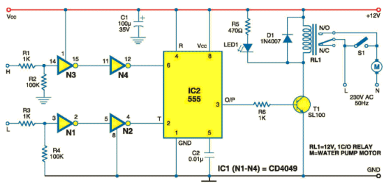
![]()
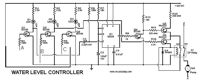
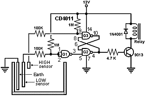
The circuit detects the level of water via three probes in a vessel. The
probes have different lengths and the resistance of the water causes the 555
to turn on the relay. The point of the discussion is this: The 100k
resistors on the input reduce the impedance of the inputs to 100k and this
means the inputs of a 555 can be used directly. They have an input impedance
higher than 100k (about 500k). The CMOS 4049 is not needed. Depending
on the conductivity of the water, the probes can be made larger or closer
together or the input resistance to the 555 can be increased to suit the new
circuit.
As I have said before. Ask yourself this simple question: Is each and every
component needed?
Try removing each item and see if the circuit works are required. Otherwise
someone else is going to simplify your design and put you out of business.
![]()
Here is an H-Bridge that will not work. The lower left-hand transistor in
the H-Bridge will not turn on:
The following circuit uses PNP transistors to drive the bridge and both
inputs must not be LOW as this will turn on all 4 transistors in the bridge
and create a SHORT-CIRCUIT: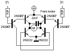
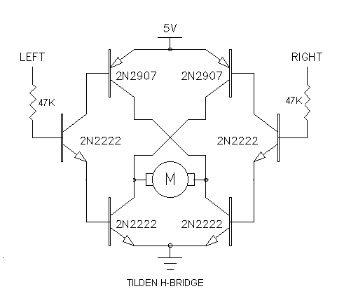
Take the left three transistors. When the input is LOW, the middle
transistor will turn on and produce a voltage of about 0.2v between the
emitter and collector leads. This will allow current to flow and turn on the
top transistor and also the lower transistor. Both these transistors will
produce a maximum of 0.7v between the base and emitter leads. Thus we
have 3 junctions across the power supply and the junctions are trying to
drop the power supply to: 0.2v + 0.7v + 0.7v . If the power
supply is higher than this voltage, an enormous current will flow and the
transistors will be destroyed.
Obviously the circuit has never been tested.
![]()
![]()
Here's another Indian circuit:
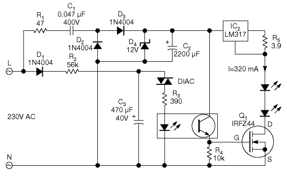
The circuit flashes LEDs and was presented in Electronics Design News. The
circuit is extremely complex for such a simple task.
The 0.047u capacitor will deliver less than 2mA RMS (5mA peak) in half-wave
and it will take a long time to store enough energy in the 2200u to produce
a flash. No LEDs will allow 320mA to flow without being damaged and a
current limiting resistor is essential. ![]()
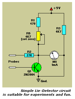 This
circuit is a simple Wheatstone bridge "lie-detector".
This
circuit is a simple Wheatstone bridge "lie-detector".
A milliammeter with its zero at the centre of the scale is connected
across the bridge. It serves as a bridge-imbalance detector. Large bare copper
boards can be used to make suitable probes.
The probes should be taped or strapped directly to the skin on the subject's
hand or arm, separated by at least 5cm. When the subject is
relaxed and his or her skin resistance reaches a stable value, adjust
potentiometer R5 to obtain a null on milliammeter M1. The subject can then
be questioned about the truth or falsity of emotionally loaded or
embarrassing subject.
The subject's skin resistance will change in response to questions if they are phrased correctly. The bridge will be unbalanced if the
subject reacts emotionally to the questions.
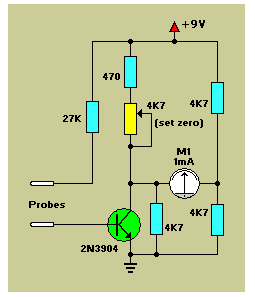
The second diagram is a bridge arrangement and the resistor across the
transistor can be removed and the pot adjusted when the probes are in place.
A simple mistake of leaving out a resistor in the bridge can render the
circuit non-functional. That's why you must build every circuit before
putting it on the web.
![]()
100v diodes are sufficient but most stores only stock 400v 1N4004
diodes.
![]()
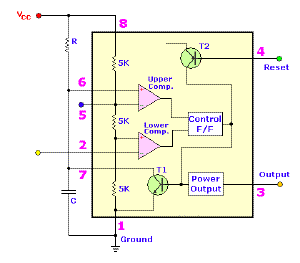
There are 3 problems with this circuit:
1. There is no "stop resistor" on the 10k pot.
2. Pin 4 of the 555 is not connected.
3. The 1k resistor is too high.
At first glance I missed the fact that no stop resistor has been included
because the diagram is not a SCHEMATIC. It is a LAYOUT DIAGRAM and you
cannot instantly see what the circuit is doing.
That's why a layout diagram is so dangerous. It does not allow you to become
instantly aware of any mistakes.
If the 10k pot is turned clockwise, pin 7 will be connected to the 9v supply
and the 555 will be immediately damaged. A 1k resistor between the end of
the pot and the 9v rail is needed.
The reset pin (pin 4 ) of the 555 is internally pulled HIGH via a 100k
resistor but this pin should not be left unconnected as it is a bad policy
to leave reset lines floating. Some chips have very high impedance reset
lines and this will cause erratic behaviour.
The 1k current limit resistor on the cathode leads of the LEDs can be
decreased to 470R to allow the maximum current to flow.
At 1k the current will be about 7mA. At 470R the current will be about 14mA.
The 10n on the supply and pin 5 will have no effect on the operation of the
circuit and are not needed.
![]()
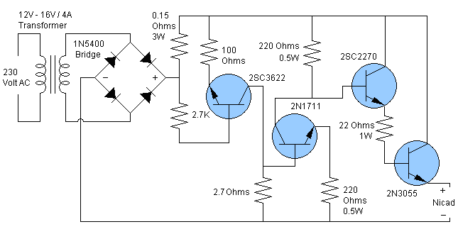
The following 6 transistor circuit flashes a red LED on a 1.5v supply. The
first two transistors form a 15kHz oscillator to charge a 0.47u electrolytic
with the aid of Q3. This circuit has been described in our "200
Transistor Circuits" eBook. The low-frequency oscillator made up of Q5
and Q6 turns the first oscillator ON and OFF to blink the LED. But the
circuit is far too complex.
Before designing any circuit, you need to research circuits that have
already been produced as you may find someone has already designed something
much simpler.
This reminds me of the original Garrard turntable with 245 components to
lift the arm onto the record and return it to the rest position at the end
of play. Then someone came along with an identical turntable using just 15
components. 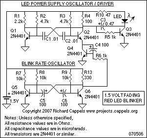
![]()
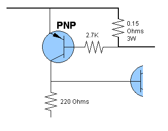
On top of this the circuit contains a number of faults. The first two
transistors are an attempt to produce a constant-current circuit to charge
the electrolytic. When the base of Q1 is connected to the collector, the
transistor turns into a diode and the circuit limits the current that
charges the electro. This may work but it uses 6 components that can be
replaced with one component.
Connecting the base to the emitter of Q4 turns the transistor OFF and it is
effectively removed from the circuit, so that Q3 is the only transistor
providing and emitter-follower function to deliver current to the LEDs. This
is a major fault in the design.
![]()
![]()
![]()
The circuit will not oscillate.
![]()
![]()
![]()
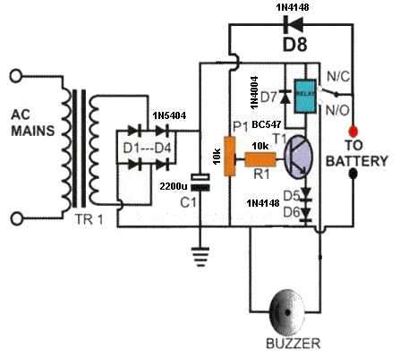
Here's a very simple circuit with a lot of mistakes. It's a very simple
automatic battery charger and the concept is very good, but the circuit
needs some improvement. The author thinks the diodes in the emitter will
increase the Hysteresis. But this is not so. As the voltage increases
on the base of the transistor, the relay pulls in when the current though
the base is high enough to activate the relay.
The two diodes simply put an extra 1.2v on the emitter, so the voltage on
the base must be about 1.8v before the transistor will begin to activate the
relay.
All the two diodes do is shift the activation-point 1.2v up the 10k pot.
D8 serves no purpose at all.
The 2200u electrolytic can be as low as 220u as very little current is being
drawn by the circuit when the battery is not connected.
The 10k should be replaced with a 1k pot to make it easier to adjust the
13.7v trigger-point to detect when the battery is charged.
The 10k base resistor can be removed and placed in the position of D8. This
means the 1k pot will have about 1v across it and this is 10 times better
than the voltage across the 10k pot. The 13.7v adjustment will be much
easier to achieve.
D7 is not needed as any spikes from the relay can be absorbed by the
transistor. It will zener at about 45v to 55v.
All the corrections to this circuit can be seen in the second diagram.
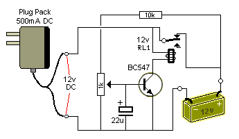
The plug pack can be 300mA, 500mA or 1A and its
current rating will depend on the size of the 12v battery you are charging.
For a 1.2AH gel cell, the charging current should be 100mA. However, this
charger is designed to keep the battery topped-up and it will deliver
current in such short bursts, that the charging current is not important.
This applies if you are keeping the battery connected while it is being
used. In this case the charger will add to the output and deliver some
current to the load while charging the battery. If you are charging a flat
cell, the current should not be more than 100mA.
For a 7AH battery, the current can be 500mA. And for a larger battery, the
current can be 1Amp.
SETTING UP
Connect the charger to a battery and place a digital meter across the
battery. Adjust the 1k pot so the relay drops out as soon as the voltage
rises to 13.7v.
Place a 100R 2watt resistor across the battery and watch the voltage drop.
The charger should turn on when the voltage drops to about 12.5v. This
voltage is not important.
The 22u stops the relay "squealing" or "hunting" when a load is connected to
the battery and the charger is charging. As the battery voltage rises, the
charging current reduces and just before the relay drops out, it squeals as
the voltage rises and falls due to the action of the relay. The 22u prevents
this "chattering".
To increase the Hysteresis: In other words, decrease the voltage where the
circuit cuts-in, add a 270R across the coil of the relay. This will increase
the current required by the transistor to activate the relay and thus
increase the gap between the two activation points. The pull-in point on the
pot will be higher and you will have re-adjust the pot, but the drop-out
point will be the same and thus the gap will be wider. In our circuit, the
cut-in voltage was 11.5v with 270R across the relay.
Note: No diode is needed across the relay because the transistor is
never fully turned off and no back EMF (spike) is produced by the relay.
![]()
This looks like a fantastic battery charger circuit until you realise the
first transistor is connected with the emitter to the positive rail and it
will zener as soon as the 12v is applied and it will have a very low
voltage across the emitter-collector AT ALL TIMES!
It's a pity the author of the site:
Here's another circuit from Electronics For You - the Indian electronics
magazine.
The NAND gate symbol on the circuit is a CD4011. A CD4001 is a NOR
gate. Three of the gates are inverters, so either chip can be used. But gate
N3 needs to be looked at. CD4011 - NAND INPUT A INPUT B OUTPUT 0 1 0 1 1 CD4001 - NOR INPUT A INPUT B OUTPUT 0 1 0 1 0
When light is falling on the
receiver, pins 12 and 13 will be HIGH. Pin11 will be LOW, making pin 9 LOW.
Pins 1 and 2 will be LOW, making pin 3 HIGH. This will put a LOW on pin 8.
Thus the inputs to the gate we are considering is: LOW - LOW If we use
a CD4011 NAND gate, you can see the output does not change if only one
input changes, and thus we need to use a NOR gate.
Another reader, with considerable experience in project-design, made the
following comments:
Most of the things that have been mentioned are basically untrue.
No LOAD Resistors
Here is another mistake from JosePino website:
NO YOU CAN'T !!
http://www.circuitdiagram.org/images/nicd-battery-charger-circuit.GIF
does
not check his circuits before adding them to the web.
The circuit needs to be re-designed as follows:
![]()
This circuit is filled with mistakes.
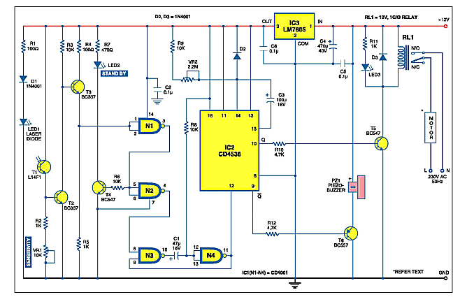
0
1
0
1
1
1
0
0
1
0
0
1
1
0
The main problem is Qbar. It rises to 5v when HIGH but this allows the BC557
transistor to have a base-emitter voltage of about 7v and this will not turn
off the piezo buzzer. To fix this, simply connect a BC547 transistor to the
piezo buzzer with 4k7 to the Q output, just like the relay-drive transistor.
The last five faults are minor.
What is the purpose of diode D1? - it serves no purpose.
T2 and T3 need not be power transistors.
The 47u on pin 10 is around the wrong way.
T3,
R4 and R5 are not needed. Theses three components form a voltage-follower
and are not needed.
![]()
I designed the following circuit to deliver 5v to a microcontroller project.
It is capable of delivering up to 50mA with 75mV ripple at about 80Hz. It
was provided as a suggestion to a reader on an electronics forum:
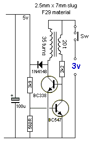
But at high frequencies the BC337 might not have enough time to turn on
hard, so there will be limit to L2 current and that means output current
will suffer. Also it needs a couple of caps on the input, the big batteries
won't supply the high freq current pulses very well, try a 100uF electro in
parallel with a 10uF tantalum on the input.
It's probably not switching fast enough too, you can add a small cap between
the collector of Q1 and the top of R3, to add a heap of positive feedback.
It might also benefit from a small cap across R3 to give you about 0.2v
ripple there to ensure a lower frequency and good turnoff of Q2.
Replacing the 1N4148 diode with a small Schottky 1N5819 that has lower
forward voltage and higher current, that will help.
It's hard to get good current and good efficiency from a 2 transistor
design, you may have to go to 2 transistors as the oscillator to ensure a
good tight square wave operation, and use a third transistor as the voltage
regulator in feedback.
The circuit was never intended to provide HIGH CURRENT. It delivers 50mA at
5v with 30mV drop and 75mV P-P noise at 80kHz.
The 2k2 reduces the impact of the gain of the transistor enormously, so an
extra-high-gain transistor is not going to be of any advantage.
The circuit has been especially designed �very lightly� so that it consumes
very little current when the output is almost zero current. At present, it
consumes 5mA.
An extra 10u tantalum electro on the input is not going to improve matters.
A 100u is perfectly sufficient across the battery. However in the original
design, the circuit delivers 50mA @5v and an electro is not needed.
Changing the diode is not going to alter the output as a 1N4148 will handle
up to 70mA.
And saying you cannot get good efficiency from a single transistor is simply
not correct. A single transistor works much better because it responds to
the requirement of the transformer much better than delivering a
long-duration square wave, that maybe over-saturating the core.
The circuit self-regulates as the input voltage drops, and turns on more to
deliver the required output.
Before making comments on an open forum, readers should build the circuit
and try the things they are suggesting.
If I didn't correct these suggestions, many readers would get a
completely-wrong picture of the workings of the circuit.![]()
You may find a microcontroller
circuit on the web that does not use LOAD RESISTORS on any of the
outputs, such as this circuit by J Pino:
The circuit has a major fault.
There are no dropper resistors to any of the LEDs in the displays.

The problem with NOT USING resistors is this:
The output is not going fully HIGH. It is only going to between 1.7v and
2.3v, depending on the colour of the LEDs in the displays. This means the FET inside the micro is dropping 2.7v to 3.3v @
25mA and this is a much higher wattage than the manufacturer of the chip
has allowed-for. The chip has been designed for 25mA from each output
but the output must be allowed to rise to nearly 5v.
With the design above, the chip can be dissipating between 460mW and
660mW.
The PIC16F84A has now been replaced by the cheaper PIC16F628A.
J Pino has updated his site with this absurd comment:
There are no resistors on most of my projects because I limit the
current using the software instead of using resistors.
He is confusing OVERALL WATTAGE REDUCTION with CURRENT LIMITING.
Software does not reduce the current. It simply reduces the time
when the current is delivered and this results in a reduction in wattage
over a period of time.
But the instantaneous currents delivered by the chip when current-limiting
resistors are omitted, can be more than the chip is designed to deliver.
For instance, a PIC chip connected directly to a LED will deliver about 33mA
and the voltage across the FET driver will be about 3v (because the FET is
not allowed to "pull-HIGH"). This gives a dissipation of 100mW. The FET will
normally dissipate 25mA and the voltage across it will be 500mV, giving a
result of 12.5mW. This is a BIG DIFFERENCE.
"You can connect the CD4050's to 12v . . . . ."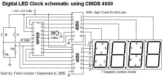
If you connect the 4050's to 12v, the input of the chip will require a
voltage higher than 6v for it to detect a HIGH and the output of the 16F628
is a maximum of 4.8v.
This is a point MISSED by J Pino because he did not test the circuit before
adding this comment to his website. Never say anything without testing the
answer, no-matter how trivial.
![]()
No Resistor
Here's another circuit from J
Pino, where he has left out a safety-resistor. When the NPN transistor turns
on, it turns on the PNP transistor and the voltage-drop across the
collector-emitter junction of the NPN transistor is very low and the voltage
drop across the base-emitter junction of the PNP transistor is 0.6v.
This causes a very high current to flow and is wasted-current.
A 10n capacitor does not have a "positive."
![]()
![]()
No Resistor - plus a resistor NOT NEEDED!
Here's another circuit from J
Pino, where he has left out a safety-resistor. J Pino's website is very
frustrating. Not only are there many mistakes in his circuits, but he does
not make it easy to copy the circuits. It's totally ignorant people like
this that we don't need on the web.
What is the point of producing a circuit if it cannot be copied and
reproduced?
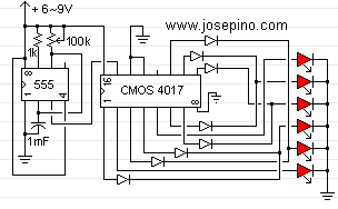
J Pino prides himself in leaving out important current-limiting resistors.
He has done it again in this circuit. The row of LEDs should have a 330R
current liming resistor so the output of the 4017 can go HIGH and deliver
about 10mA to the LED that is illuminated at the particular instant.
However the most noticeable point about his ignorance in designing a circuit
is the 1k resistor on pin 7 of the 555. This is not needed. The circuit will
not work with pin 6 going to the positive rail. And 1mF is 1,000uF.
This is a very large value for this type of circuit.
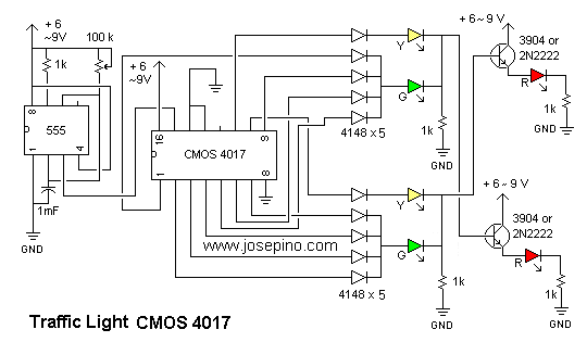
![]()
No Output
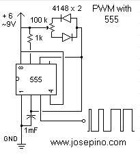
Here's another one from J Pino. He has
not checked the circuit. It will not work. See
50 - 555
Circuits for the correct way to create a PWM circuit. It has been on his
website for 5 years and no-one has made the circuit because you cannot copy
the images!
Only a moron would create a website that cannot be copied! What is the point
in providing information that needs to be copied to be reproduced, and not
allow the circuit to be copied?
![]()
No Output
While on the topic of J Pino's
website. Here's another one. Apart from the fact that the 555 circuit will
not work, the emitter-follower transistor is not needed.
See The
Transistor Amplifier on how to design transistor circuits.
The lower diagram shows the voltage-drops from the output of the 4017 and
you will see how much voltage remains from a 6v supply, to drive the red
LED. This circuit has obviously NEVER been tested and should not be
presented on the web for others to get frustrated over.
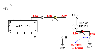
The diagram above shows the voltage-drops from
the output of the IC to the red LED. It does not matter if the collector of
the emitter-follower is connected to the 6v rail, the emitter cannot be
higher than the input voltage and this circuit provides 0.5v across a 1k
resistor to deliver 0.5mA to the red LED.
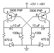
![]()
Another J Pino's mistake.
The electrolytics are around the wring way. The base is always just below
rail voltage the end of the electrolytic connecting to the base should be
the positive of the electrolytic.
![]()
Another J Pino's mistake. The
electret mic is connected directly to an output pin. The pin is taken HIGH
then the pin is made and input and the time taken to discharge the 10n is
recorded. There is no resistor in series with the 10n to provide a "time
delay" and an electret mic should never be connected directly to a 3v or 5v
supply.
There is no "electronics understanding" behind this feature.
LED!!!
MICRO BUG
By re-arranging the components we see the circuit is a normal FM transmitter
but the 20p trim cap is connected to the negative rail. This will work just
as effectively as connected to the positive rail however the position of the
component does not make it obvious the 20p and coil are in an arrangement
called a TANK CIRCUIT and this is the most important part of the circuit as
these two components have a natural capability to oscillate and produce a
sine-wave, when a small amount of energy is delivered to them. Not only do
they oscillate, but they produce a waveform that can be considerably higher
than the delivered-voltage.
1-AMP POWER SUPPLY MODULE
THE DANGERS OF USING A "LED WIZARD"
The characteristic voltage (the colour of the LED) is not important in this
discussion. Obviously white LEDs will not work as they require 3.4v to 3.6v
to operate.
More EFY mistakes:
The circuit is far too complex. The .22u allows about 15mA to enter the
circuit. This gives 7mA for each string of white LEDs, Hardly enough to
bother about. The LED should have been in series.
The 555 is placed in toggle mode and the author of the circuit has had to
use a relay to activate the chip.
Page 1
Page 2
Page 3
Page 4
Page 5
Page 6
Page 7
Page 8
Page 9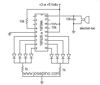
![]()
Here's another fault.
The LED is up-side-down!!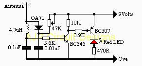
![]()
I have mentioned, so many
times, the importance of drawing a circuit
Here is a circuit, that is a total mess: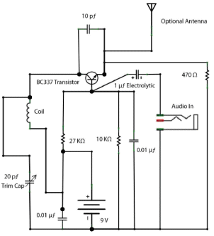
This is one of the most amazing things in electronics and when it was
discovered, (over a hundred years ago), it changed electronics completely.
It was the birth of RADIO. The only other complaint is the type of
transistor. A BC337 is a power transistor and not really suited to high
frequency.
![]()
Here is a major mistake from two different suppliers. Both modules use a
3-terminal regulator to reduce the input voltage to 5v and/or 3.3v and they
specify the current capability of the module is 1AMP! . Neither module has
any heatsinking on the regulator and neither designer has any idea of the
heat produced when a current of 1 amp flows.
Here is a lesson to be learned: When a diode is passing 500mA, it gets very
hot. When it is passing 700mA, you cannot hold your fingers on it. When it
passes 1 amp, you can boil water on the leads.
This is the sort of temperatures we are talking about when approx 0.65v is
dropped across the diode at 500mA. The voltage drop increases to 0.75v at
700mA and increases to 0.95v at 1A.
That's why the temperature rises so much. The diode is dissipating nearly 1
watt when 1 amp flows.
To prevent the diode being damaged, the leads must be short and connected to
lands on a circuit board to take away the heat.
Now we come to the 3-terminal regulator.
It needs at least 1.5v across it to provide regulation. This means the
minimum wattage being dissipated will be 1.5watts.
Neither board has any form of effective heatsink and the component will
definitely BOIL WATER.
In most cases the input voltage will be 3v to 15v higher than the output
voltage and you can imagine the heat being generated. The only way to
prevent the regulator DE-SOLDERING ITSELF, is to reduce the current.
Neither of these power supplies will be able to deliver more than a few
hundred milliamps (or less). They are extremely badly designed. They should
provide the ability to heatsink the regulator - as it will need heatsinking
in most cases.
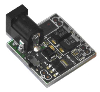
Power Supply from Embedded Adventures.com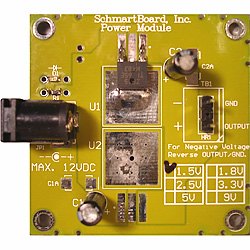
Power Supply from SchmartBoard. Inc
![]()
Here is an example, provided by a reader. Can you see the major fault?
The main fault is the dropper resistor.
Read our article on
LEDs.
The most important component is the DROPPER RESISTOR.
It must allow for the difference between the maximum and minimum supply
voltage and ALSO the maximum and minimum CHARACTERISTIC VOLTAGE of the
string of LEDs.
When we say a red LED has a CHARACTERISTIC VOLTAGE of 1.7v, we need to
measure the exact maximum and minimum value for the LEDs we are installing.
Some high-bright and super-high-bright LEDs have a Characteristic Voltage of
1.6v to 1.8v and this will make a big difference when you have 8 LEDs in
series.
Secondly, the 12v supply may rise to 13.6v when the battery is being charged
and fall to 10.8v at the end of its life.
Thirdly, you need to know the current required by the LEDs.
The normal value is 17mA for long life.
This can rise to 20mA but must not go higher than 25mA
You should also look at the minimum current. Many high-bright LEDs will
perform perfectly on 5-10mA and become TOO BRIGHT on 20mA.
As you can see, it is much more complex than a WIZARD can handle.
That's why it produced the absurd result above.
The maximum characteristic voltage for 8 red LEDs is 8x1.8v = 14.4v
This means you can only put 6 LEDs in series. = 10.8v
The LEDs will totally die when the battery reaches 10.8v
The value of the dropper resistor for 6 LEDs and a supply of 12v @20mA = 60
ohms. When the battery voltage rises to 13.6v during charging, the current
will be: 46mA. This is too high.
The CURRENT LIMITING resistor is too low.
We need to have a higher-value CURRENT LIMITING resistor and fewer LEDs.
Use 5 LEDs:
The characteristic voltage for 5 LEDs will be: 5 x 1.7v = 8.5v
Allow a current of 20mA when the supply is 12.6v Dropper
resistor = 200 ohms.
Current at 10.8v will be 11mA. And current at 13.6v will be 25mA
Now you can see why the value of the CURRENT LIMITING RESISTOR has to be so
high.
![]()
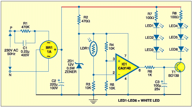
But the biggest mistake is adding an earth to the project. This will create
a SHORT CIRCUIT if the "P" and "N" wires of the mains are reversed by
accident.
The BD139 can be replaced by an ordinary low-current transistor and the IC
can be omitted and the LDR connected directly to the transistor.
In all, this circuit is a disaster in design and shows how NOT to design a
circuit..
The Author D Mohan Kumar has proven to be a disaster in designing circuits
and should not be given the space in an electronics magazine.
![]()
More EFY mistakes:
This is one of the worst designs ever. The wrong chip has been used and the
relay is a poor inclusion.
The chip should be a flip-flop in toggle mode and the relay is not needed.
This is another poor Indian design and shows the lack of
understanding of electronics. The magazine Electronics For You needs
harsh criticism. ![]()
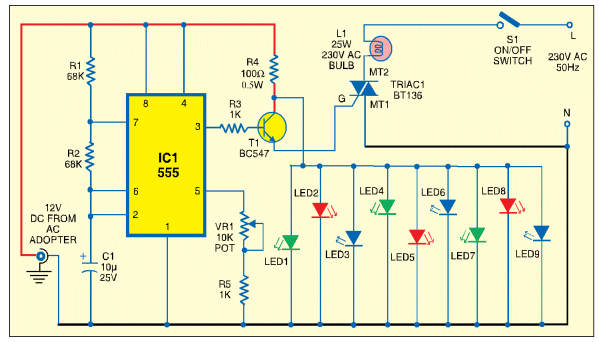
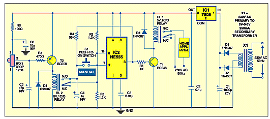
Another EFY disaster:
The circuit turns on the music chip after 30 seconds, or 60 seconds, etc to
4min 30 seconds.
I cannot think who would want this feature but the circuit is over-designed
and takes more than 10mA when sitting around doing nothing. It then plays
the same tune after every 4.5 minutes and the rotary switch has no purpose.
The circuit is badly designed and is a typical Indian disaster.
It just needs a two-transistor delay (timer) and a pot - connected to
the chip.
![]()
Another EFY disaster:
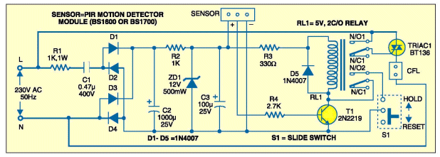
The 0.47u capacitor on the input will deliver a maximum of 35mA. The current
required by the relay is not known but suppose it is a 50mA device. This
means it has a resistance of 100R. The 330R resistor on the 12v supply, when
combined with a 100R relay will pass just 28mA. The relay will not work.
Suppose the relay is a 30mA type, the 330R combined with a 170R relay will
pass 24mA. The relay may work, but it is very special type.
The whole circuit is badly designed and the resistance of the relay is very
important. The circuit has never been tested and omitting the resistance
(impedance) of the relay is a major mistake.
Every circuit in Electronics For You magazine has a mistake and
should be avoided.
![]()
Page 10 . . . . .
Page 12