SPOT
THE MISTAKES!
Page 10

PR4401 1-watt LED Driver
by TA Babu (India)
This is one of the worst circuits I have seen. It uses a PR4401 to drive a
BD140 from a 1.5v battery.
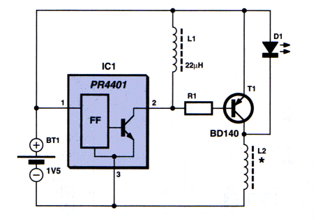
The PR4401 normally drives a LED with 20 -
40mA from a 1.5v cell and will operate to 0.9v.
The chip and circuitry is about 85% efficient but when an extra inductor is
involved and BD140, the efficiency drops to about 70%.
On top of this, the energy from a cell when trying to deliver 1watt, is only
about 60%. Putting this all together gives a very poor result. The current
from the battery will be more than 1AMP! Show me a single cell
that will deliver 1AMP. This is really an absurd way to go about things.
It would have been much better to use 4 cells and drive the 1-watt LED via a
buck regulator (current-limiting arrangement).
The cost of the PR4401 is about 60˘ to 80˘ and I have yet to see it in a
product - other than in a hobby circuit or an absurd design like this.
An equivalent IC (chip) has come on the market for 10 cents and it is a
better chip.
Here is the circuit for QX5252F:
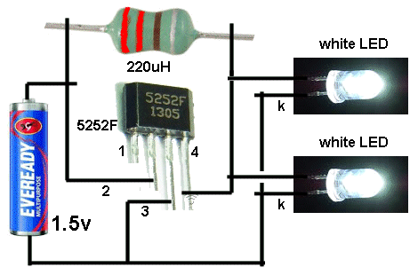
Using 220uH, the circuit takes 13mA an illuminates 2 white LEDs very
brightly.
Using 100uH the circuit takes 30mA and the LEDs are really the same
brightness.
Using 33uH the circuit takes 80mA and the LEDs are just about the same
brightness.
Obviously the 220uH creates the most efficient circuit.
The PR4401 only delivers about 20mA. The QX5252F delivers more than
100mA.
Here's a circuit from "All About Circuits:"
It has four technical faults; Can you spot them?
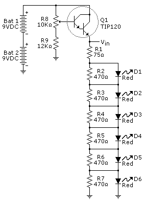
Firstly the Darlington transistor is not needed. It
can be an ordinary transistor. And it doesn't have to be a "power"
transistor. The circuit is taking a maximum of 25mA
Secondly, the 75R current limit resistor does not give very much tolerance
for changes in supply voltage. A change of 1v will alter the current through
the LEDs by 13mA. Most LEDs run on 15-25mA MAX and if the voltage drops by
1v, they will dim considerably.
Tthirdly, the 470R resistors do NOTHING.
But the biggest mistake is the WHOLE CIRCUIT. As you adjust the pot, the
voltage starts at 9.8v and the 6 LEDs require 10.2v. So none of the LEDs
illuminate. When the pot is turned to 10.2 + 1.9v the LEDs are taking 25mA
and this is the maximum allowable. This means the pot is turned 1.9/7.8 = 65
degrees before the LEDS "burn out." What a disastrous circuit!
I also have another point of disagreement. Why use 18v to drive 6 LEDs.
Since only about 11v is needed, you are wasting over 40% of the energy from
the batteries.
You could drive 8 LEDs from a single battery as 4 LEDs in one string and 4
LEDs in a second string, and use less energy.
If you are going to design a circuit and add components such as the 470R
resistors above, test the circuit to see if
they have any effect.
This is one of the last things I do when designing a new circuit.
I gradually remove each component to see if it has any effect. Sometimes I
have removed over 10 components that had little or no effect on the
performance.
And sometimes a re-design results in 3 or 4 fewer components.
It's very embarrassing to find someone has omitted 10 components and the
circuit works exactly the same.
Don't let this happen to you. Ask yourself, "What is each component doing?"
This circuit has obviously NEVER BEEN TESTED.
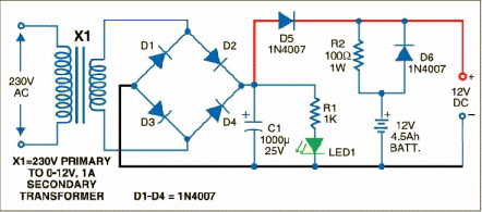
Here's another circuit from Electronics For You, an Indian
publication. It appears to be correct, until you see the 100R resistor
charging the battery.
The transformer is 0-12v AC
and this will produce a DC voltage at
least 18v-20v after rectification, on no load or when powering the alarm
during normal conditions. (It could be as high as 22v).
This voltage is far too high for a 12v battery and it will cause gassing and
the battery will dry out in a few months.
It is absolutely essential to charge the battery until its voltage reaches
14.1volts then turn-off the charging voltage so that the battery does not
produce bubbles. This circuit does not do that.
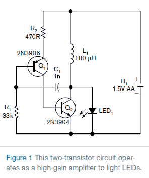
Here's a simple circuit that was improved 50% by
simply changing the position of one component. The original current was
30mA. After changing the position of the 470R resistor, the current dropped
to 17mA with the same brightness from the white LED.
The reason is simple.
In the first circuit, the BC557 is acting as an emitter-follower to the
signal (current) delivered by the 1n and it is taking much longer for the
two transistors to turn on. In the second circuit, the two transistors turn
on much faster and less wasted current passes though the inductor.
(Even the wording for Figure 1 in the fig below, is misleading. The LED is illuminated by the
spike produced by the reverse-voltage from the collapsing magnetic flux of
the inductor - the 2-transistor amplifier is merely the driving mechanism.)
Here's a circuit that was designed from a simulation software package. While
these packages are fairly good, they do not contain all the data and
mysteries that come with actually using a component.
I have found some BC547 transistors that do not work in 88MHz FM
transmitters. And some 74c14 ICs that produce a different frequency in an
oscillator. These irregularities are never covered any any simulation
package.
You must build a circuit to prove its reliability and operation. |
|
The fault with the above circuit lies in the fact that the output of a 555
is about 0.2v to 0.5v above the negative rail when outputting a LOW.
When this is combined with a gating diode, it produces a voltage of about
0.8v on the base of the driver transistor and this will NEVER turn the
transistor OFF.
The remedy is to include a voltage-divider network made up of two resistors.
In the following example, the 470R between base and 0v and 470R between base
and gating diode, form a voltage divider. The best way to see their
operation is to remove the buffer transistor.
To produce 0.6v on the join of these two resistors we need to supply 1.2v at
the top.
This is what is now needed to turn ON the transistor and if the gating diode
produces a voltage of 0.8v, the transistor will see 0.4v and it will turn
OFF.
This next mistake highlights the need to draw a circuit so that it is
immediately obvious how the circuit works.
At first impression, the first circuit appears to be scanning the LEDs in a
3x4 matrix, as the LEDs are all drawn in the same direction:
However when the LEDs are re-drawn as shown in the following circuit, we can
see the arrangement is known as Charlie-Plexing.
Here's a circuit with a couple of mistakes:
It operates as follows:
The Red LED illuminates if the voltage is below about 12.5 volts.
The Green LED begins to light at about 12.5v and the Red LED fades, at about
14.25v the Yellow LED begins to come on and by 14.75v the Green LED has
faded out.
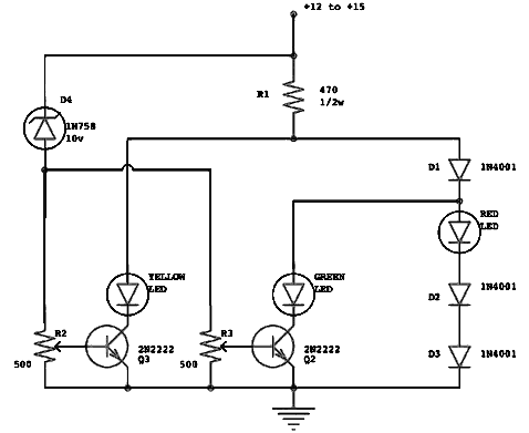
If the pots are turned to one end; the zener, pot and transistor will be
damaged. A 1k resistor needs to be placed between the base and wiper of the
each pot.
Here is a circuit designed by Talking Electronics to monitor a battery:
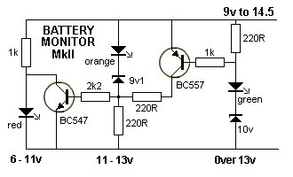
The red LED turns on from 6v to below 11v.
It turns off above 11v and the orange LED illuminates between 11v and 13v.
It turns off above 13v and the green LED illuminates above 13v
Here's another circuit from Electronics For You, and Indian
publication:
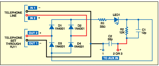
The first thing I have always said is this: Always draw a circuit so that it is
easy to understand. I have absolutely no idea what the 4 diodes are doing
and how the circuit is actually connected to the two phones.
By re-drawing the circuit, this is much easier to see:
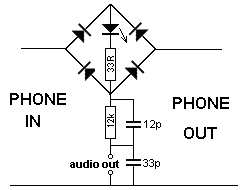
The 4 diodes are a bridge and the LED is turned on when the phone is picked up.
The circuit can be connected to the phone line either way as the diodes are
wired so that the LED always illuminates. But the 33R has no effect at all
and can be removed.
Secondly, the 12p and 33p have no effect on the audio. They should be in the
range 10n to 100n to have any effect at audio frequencies.
And yet another circuit from an Indian website:
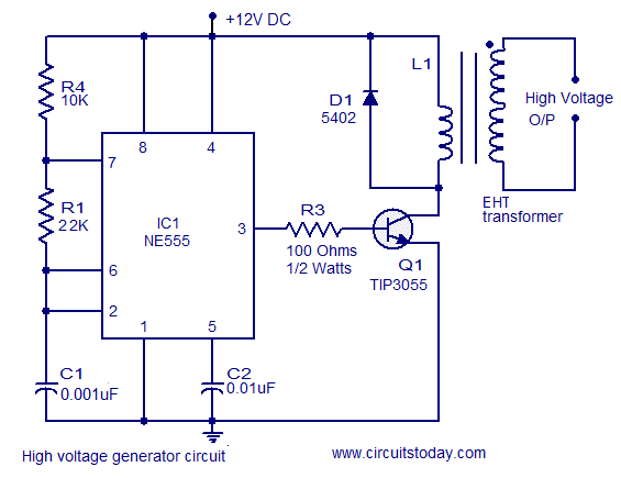
The EHT transformer will only produce 8kv-10kv when used in flyback mode.
This requires the transistor to turn off very quickly at the time when the
transformer is reaching saturation. It is very important that the timing for
the transistor is accurately controlled and this requires a feedback signal
from the transformer. This circuit does not provide that feature.
Secondly, NO TRANSFORMER is going to produce an extra high voltage when a
diode is connected across the primary. This diode will completely absorb the
energy from the collapsing magnetic flux and prevent a high voltage being
produced.
Nearly every circuit from CircuitsToday has a fault as nothing is tested
before being written up on the web.
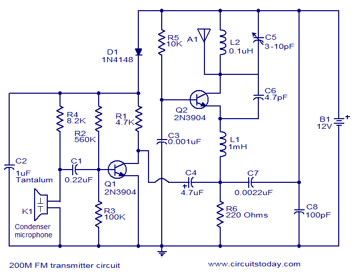
More from CircuitsToday.com:
|
|
There are many faults with this circuit.
1. The 1u tantalum can be an ordinary electrolytic.
2. The 8k2 resistor should be about 47k
3. The 220n should be about 22n
4. The diode does not serve any purpose.
5. The 10k resistor should be at least 47k
6. The 0.1uH should be about 0.06uH
7. The 3-10p should be at least 22p
8. The 100p across the battery should be at least 22n.
9. The 220R resistor should be at least 470R
See our series on designing FM transmitters and you will learn how to design
circuits like this and not make the mistakes contained in this circuit.
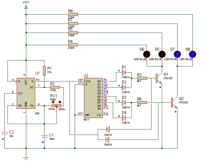
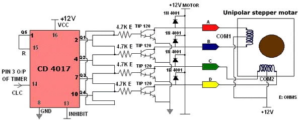
Here we have a 4017 driving 4 buffer transistors.
If you look carefully, you will see the 4 outputs of the 4017 are connected
together.
Each output of a 4017 is bi-polar. In other words it drives HIGH or LOW. At
12v, each output will deliver about 100mA when driving a short-circuit. When
one output is HIGH, it is driving three LOW outputs and this will put
considerable strain on the chip. In the following circuit, each output will
rise to about 3v and that is why the designer thought the circuit would work. But
this voltage is produced under enormous strain inside the chip. The outputs
should have either gating diodes or resistors to prevent overload.
The designer of the circuit considered the chip and stepper motor would take
zero current when the chip is reset, (the 6th output - pin 1 - goes to
reset) but he did not provide any feedback from the 4017 to tell the
oscillator when to stop providing clock pulses. If the 4017 sits with
any output HIGH, the current consumption would be considerable.
Secondly, the circuit would NEVER work as ALL THE OUTPUTS are connected
together and all the Darlington transistors are turned on AT THE SAME TIME!
I have also asked him how the circuit guarantees to remain in reset mode
when not required. In other words, what happens if the 4017 receives 3
pulses (or any of 3+5+5+5 etc). There needs to be feedback from the
4017 to tell the "clock" when to stop sending pulses. In other words, the
clock needs to know where the 4017 is.
I have contacted the author of the circuit: shoumik banerjee
schawn143@yahoo.com and he now
claims the circuit has never been tested. Only a fool puts a project on the
web without building and testing it. Not only that, but it is totally unfair
to other readers, who may build the circuit and find it has no chance of
working. That's why you have to be careful with everything you find on
the web.
I have seen some "impossible" circuits that work and some that should work,
but don't.
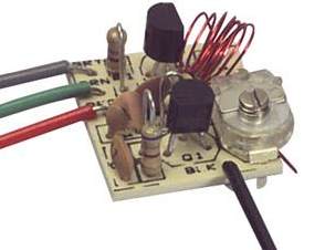
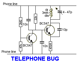
TELEPHONE BUG
Look at the coil. A floppy coil like this is totally unsuitable as it will
be "telephonic." This means it will vibrate when bumped and will even pick
up sounds such as talking, music and footsteps, and transmit them, just like
a microphone. I suggest you build this circuit and use 7 turns of thin wire
on an 8-10mm pen and see how the coil picks up every sound in the room.
Simply connect a 9v supply and the circuit will work. The coil should be 6t
and 3mm diameter.
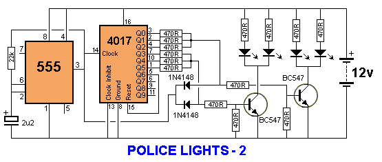
Here's another CircuitsToday.com disaster:
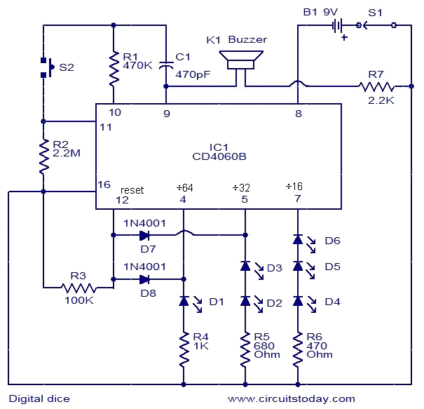
Apart from the circuit being up-side-down and difficult to work out how it
operates, output pin 7 will illuminate 3 LEDs more often than pin 4
with the single LED. In fact the Digital Dice is biased by an amount of 4:1
and is totally unsuitable for any game that requires an unbiased dice.
Another INDIAN disaster:
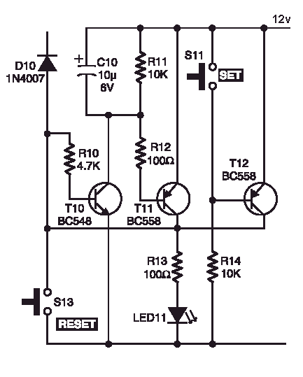
Note: the RESET switch shorts transistors T11 and T12 across the power
rails. This is a very bad design fault and could be improved by placing the
RESET switch between the base of T10 and 0v rail.
Here's another circuit from Electronics For You, the Indian
publication:
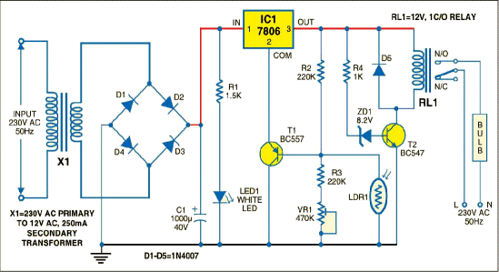
The relay is activated when light ceases to fall on the LDR. The resistance
of the LDR increases and the BC557 transistor turns off. This allows the
voltage on the common terminal of the 7806 to rise and the output voltage
rises.
When the voltage rises above 9v, the base of the BC547 sees a turn-on
voltage and the relay is energised.
This is a very complex circuit to perform such as simple task.
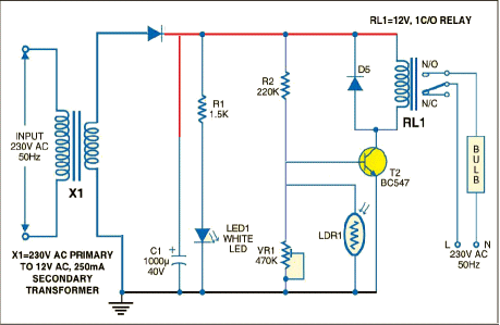
A much simpler circuit is shown below:
Here's a circuit from a renowned electronics writer.
It can be simplified considerably by realising the fact that the voltage
drop across 4 LEDs is greater than 5v and they will not illuminate when not
required. |
|
Here is a simplified diagram: The extra LEDs in series with "A's" are to
prevent the "A" LEDs illuminating when not required. They are not used on the display. |
|
Here's another CircuitsToday.com disaster:
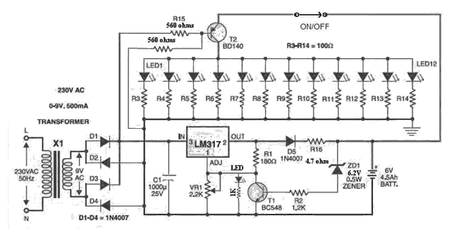
The circuit takes 300mA. By placing 3 LEDs in series, the current will be
reduced to 100mA. This is a 300% improvement. On top of this, many of the
parts can be removed and the circuit simplified considerably. You have to
"think outside the box" after designing a circuit and ask yourself: Can the
circuit be simplified?
Here are two mistakes from DayCounter.com
http://www.daycounter.com/Circuits/Latching-Momentary-Switch/Latching-Momentary-Switch.phtml
http://www.daycounter.com/Circuits/Transformerless-Power-Supplies/Transformerless-Power-Supplies.phtml
I informed them of the mistakes and received NO REPLY.
The first circuit had no resistor on the base of Q2. When Q1 and Q2 are
turned on, a very large current will flow through the emitter-collector
junction of Q1 and base-emitter junction of Q2. Both transistors will be
damaged. The 10k resistor limits this current.
When the circuit is turned on, capacitor C1
charges via the two 470k resistors. When the switch is pressed, the voltage
on C1 is passed to Q3 to turn it on. This turns on Q1 and the voltage
developed across R7 will keep Q1 turned on when the button is released.
Q2 is also turned on during this time and it discharges the capacitor. When
the switch is pressed again, the capacitor is in a discharged state and this
zero voltage will be passed to Q3 turn it off. This turns off Q1 and Q2 and
the capacitor begins to charge again to repeat the cycle.
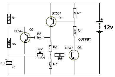
LATCHING A PUSH BUTTON
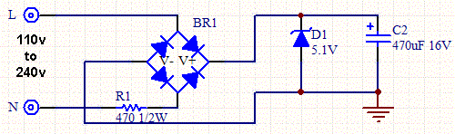
The second circuit shows a 470R 0.25watt resistor on the input. Even if
the input voltage is 50v, the power dissipated by the resistor will be
5watt. Imagine the power-loss at 110v or 240v!!!!
We already know that a resistive power-supply is very inefficient and
requires a very large resistor to drop the voltage, but obviously DayCounter.com
has no idea.
See The Power Supply article on left Index for more details on
capacitor-input and resistor-input power supplies.
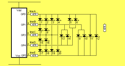
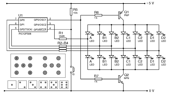
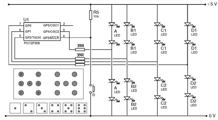
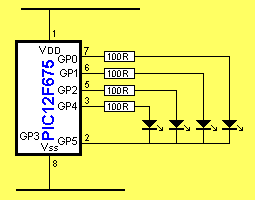
A MICROCONTROLLER CIRCUIT
This circuit drives 4 LEDs via 4 output lines with sinking via a single line
on the microcontroller.
Each line can only sink or source 25mA. If GP0 is HIGH and GP5 LOW, the last
LED will illuminate.
If GP1 is made HIGH, the two outputs will be able to deliver 25mA each to
the LEDs (if the circuit was designed correctly) but GP5 will ALWAYS only be
able to sink 25mA. The result is this: The two output lines will PULL HIGH
but GP5 will not be able to go fully LOW and the result will be about 12mA
to 15mA through each LED. If the other two outputs go HIGH, GP5 will not
pull very LOW at all and only about 6-8mA will flow in each LED.
The sinking line is the limitation and this type of circuit is to be avoided
if you want each LED to be fully illuminated.
AUTOMATIC LIGHT
Here's another circuit from Electronics For You, an Indian
publication. Many of their circuits have obviously NEVER been tested. This
one is dangerous.
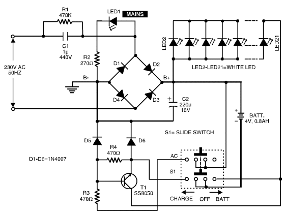
There are two major faults with the design. Can you spot them?
1. When the circuit is off, what is to stop the 220u charging to a very high
voltage and blowing up? - Absolutely NOTHING!
2. The 3v6 white LEDs are being placed directly across a 4v supply without
any current-limiting resistor. They will be damaged.
The circuit is so badly laid out that it is impossible to see what is
happening.
The earth symbol should NOT be included. If the earth symbol is connect to
the earth-lead of the power-flex and the AC lines are connected incorrectly,
the project will short-circuit via via D4. This is a major mistake.
The circuit performs like this: When the AC fails, the LEDs will
illuminate.
I don't like the idea of a transformerless power supply. The circuit should be
connected to a 12v plug pack. However, here are the corrections and a better
layout:
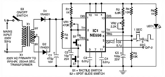
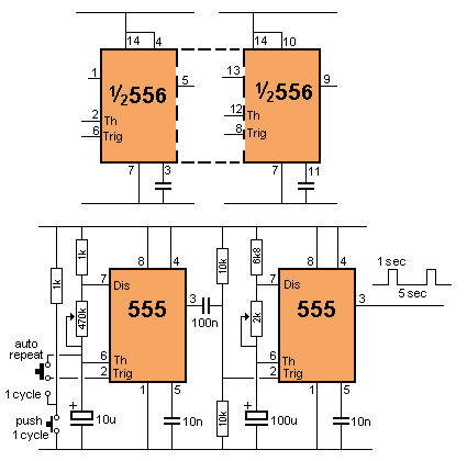
PULSES
The next circuit does not have any mistakes in the design but the layout
could be a lot clearer if two separate 555 blocks are used to show how it
works. Most hobbyists will have 555's in their parts-box, and this is why
they should be specified. We have also shown how a 556 is separated into two
555's and the pin numbering:
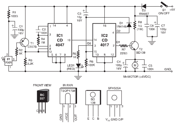
IR REMOTE ON/OFF FOR MOTOR
Another circuit from Electronics For You, the Indian publication. It
uses a TV remote control to turn a motor on and off. Any button can be used
to provide the action. However it
is over-designed and the drive to the motor should be common-emitter.
When using an emitter-follower, the emitter
voltage will be less than rail voltage by a number of factors.
There are three voltage-drops:
The output of the chip will be less than rail voltage by about 200mV. The
voltage drop across the 220R resistor will be 250mV and the drop across the
transistor will be base-emitter voltage plus the 200mV and 250mV, making the
total about 1,100mV for 100mA current-flow.
As the current increases, this voltage-drop will increase and the
combination of the voltage-drop and current-flow will heat up the transistor
considerably.
By converting to a common-emitter design, the collector-emitter voltage is
less than 50mV for 200mA current.
This is an enormous difference.
In addition, pin 12 should never be connected to 0v rail. It is an output
pin (carry out).
The circuit can be simplified as shown in the second design. The 22k and 10u
form a delay circuit to slowly charge the 10u and on the rising wave-form,
the 4017 clocks to the next output. The 10u and 22k also prevent the
"repeat" signals from the remote control clocking the chip many times.
If you keep your finger pressed, the chip clocks only once. Do not use
Philips 74C4017IC. It did not work. The IR receiver used in the
second circuit had pinout: 1: output
2: earth 3: supply rail. All the IR receivers are different.
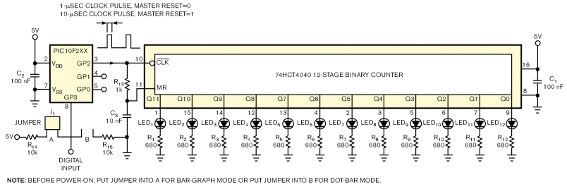
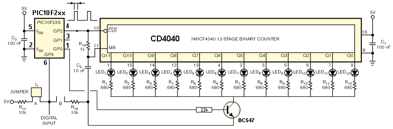
Here is a design from Electronics Design News:
http://www.edn.com/article/457607-Drive_12_LEDs_with_one_I_O_line.php#id3861137-39-a
The design is very good however it suffers from a lot of flickering as the 4040 counter is filled with
values via a clocking action.
The CD4040 chip is simply a counter (called a binary counter or divider) and for each clock cycle,
the lowest output goes HIGH then LOW.
With 12 outputs, it takes up to 4,096 (but more likely about 1,000) cycles to produce a result. This
may take only a few milliseconds but will produce a slight flicker on the screen.
This can be eliminated by connecting all the 680R current-limiting resistors to a common-emitter transistor
and connecting the base of the transistor to one of the outputs of the micro.
The project uses the 6pin PIC10F202 (or similar) micro with 3 in-out lines and one input line.
The project also uses a clever technique of pulsing the clock line HIGH for 10uS and this will allow the
reset line to rise and reset the chip. This will also clock the chip once and this has to be taken into account.
The assembly code for the project is also included.
The program detects either dot mode or bar mode by placing a jumper between 0v and GP3 or +5v and GP3.
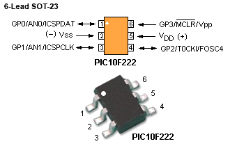
The circuit states a PIC10F2xx is used and the pinout is shown below
with a BC547 transistor used to create "blanking."
The program is not complete. It does not automatically detect a HIGH or LOW on GP3 for dot or bar mode.
It does not have any value for the number of LEDs to be displayed and it does not have any instructions for
the sinking transistor. However the concept can be used and it expands 3 lines of a micro to 12. |
; LISTING1.ASM: dotbar/bargraph assembler routine
;-------------- define hardware ----------
#define	 CLK	GPIO,2
;-------------- define variables ---------
	CBLOCK	0x08	; beginning of RAM (PIC10F202/206)
	power		;=1,2,...,12 numero of LED to light on
	cntL,cntH	;low byte, high byte, for a 16 bit cnt pulses
	mode		; 0 => dotbar mode (input GP3 with pulldown resistor)
			; 1 => bargraph mode (input GP3 with pullup resistor)
	ENDC
;----------------------------------------
; HCT4040:
; if mode=0 (dotbar), then W contains numero of the LED to light on
; if mode=1 (bargraph), then W contains numbers of LEDs to light on
;-------------------------------------
HCT4040
	MOVWF	power		; power = # of LED to light on
;first, reset the HCT4040
	BSF	CLK		; GP2 = 1
	CALL	Delay10us	; fill capacitor C3 until 4040=1
	BCF	CLK		; GP2 = 0
	CALL	Delay10us	; discharge capacitor C3 => 4040=0

;then, compute: 16 bits(cntH,cntL) = 2 ** (power - 1)
	CLRF	cntL
	CLRF	cntH
	BSF	STATUS, C
decaler
	RLF	cntL, f
	RLF	cntH, f
	DECFSZ	power, f
	GOTO	majCarry
	GOTO	sendPulses
majCarry
	MOVLW	.1
	SUBWF	mode, w		; w = mode - 1
	BTFSC	STATUS, C	; w < 0 ?
	NOP			; no, w >= 0 (i.e. mode=1, & CARRY=1)
	GOTO	decaler

sendPulses
;finally, send clock pulses
	MOVLW	.1
	GOTO	nextcnt
impulse
	BSF	CLK	; GP2 = 1
	BCF	CLK	; GP2 = 0 => 1 us positive clock pulse
nextcnt
	SUBWF	cntL, f		; cntL = cntL - 1
	BTFSC	STATUS, C	; cntL < 0 ?
	GOTO	impulse		; no. (i.e. cntL >= 0)

	SUBWF	cntH, f		; cntH = cntH - 1
	BTFSC	STATUS, C	; cntH < 0 ?
	GOTO	impulse		; no. (i.e. cntH >= 0)

	RETLW	00h
;====================================
; how to call this routine:
	MOVLW	.7	; if dotbar, LED #7 lights on; if bargraph, 7 LEDs light on
	CALL	HCT4040 ; dotbar mode, if mode=0 (i.e. GP3 with pulldown resistor)
			; bargraph mode, if mode=1 (i.e. GP3 with pullup resistor)
|
|