Here's a circuit with a slight fault:
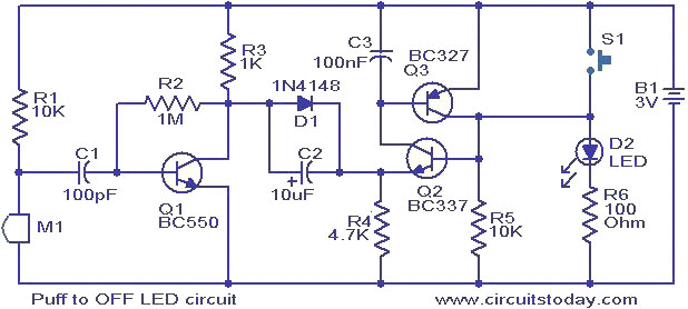
The 100p between the microphone and base of the first transistor
will not pass any waveform. It needs to be 100n.
It's obvious the circuit has never been tested.
The only other change is the removal of the diode. It changes the
flickering effect and makes the circuit more realistic.
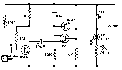
We call this circuit a "fun" circuit. Here is the corrected circuit:
See more
VOX circuits in The Transistor
Amplifier eBook.
The next example is only a simple mistake but it emphases the fact that you should draw things in a way that they are instantly recognizable. The following has a mistake and no-one in the electronics forum picked it up.
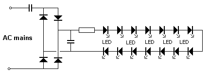
One diode in the bridge is around the wrong way.
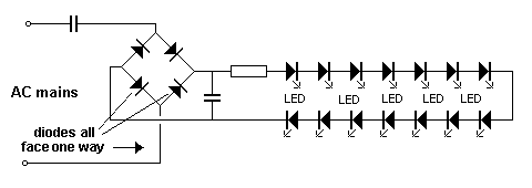
The bridge should be drawn as follows:
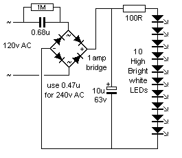
Another circuit from circuitstoday.com:
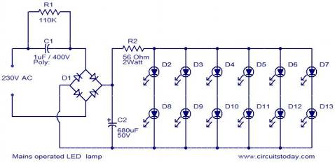
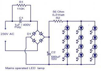
The 1u capacitor will only deliver about 60 - 70mA and a white LED needs about 17 - 20mA for good brightness. By simply re-arranging the LEDs, the circuit will work much better:
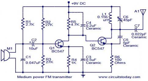
Here is a circuit of a 2-Transistor FM transmitter. It has a number
of mistakes in the design.
See Voyager project for a
well-designed circuit.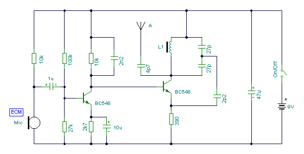
The load resistance for the microphone is too low. It will cause the
microphone to have a very high gain and create a self-oscillating
front-end.
The 1u coupling capacitor does not need to be higher than 22n. A ceramic
is quite suitable for this.
The two stages should not be direct coupled. The oscillator stage should
be self-biased so that it creates its own biasing. A "forced bias" does
not allow the transistor to operate in its best set of parameters.
The tapping between the two 27p's gives a very small signal to the
emitter. The 2p2 should tap off the collector. The parallel 27p's gives
a value of 13p, whereas the capacitance across the inductor should be
about 47p for the best "Q" for the tank circuit. No value has been given
for L1. It should be 5 turns 0.25mm wire 3mm dia.
The 47u across the battery is not needed. It should be replaced with 22n
to tighten up the rails for the 100MHz oscillator.
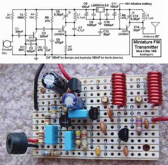
Next we have an FM transmitter that looks to be
well-designed. Apart from the complex circuit, there are a number of
fundamentally incorrect features that make the circuit unreliable.
And the layout is one of the worst I have seen for an FM transmitter.
This type of circuit should NEVER be laid out on strip-board and any
type of board that has extra conductive lines as they create "wires"
that radiate signal and they can be so effective that all the signal is
radiated and none is retained to keep the oscillator in a state of
oscillation. That's why this type of layout can result in non-operation.
The first item we will look at is the "Q" of the tank circuit.
This is a factor known as "Quality" and comes from the fact that an
inductor will produce a voltage (of opposite polarity) that can be many
times higher than the voltage applied to it.
And that's what a circuit like this FM transmitter does. The voltage
produced by the capacitor and parallel inductor on the collector, will
produce a voltage many times higher than the 5v on the rail.
These two components are called a TANK CIRCUIT and to get them to
produce a high voltage, the energy stored (and released) by the
capacitor must be equal to that of the inductor. The two work like
tipping water from one jug to another of the same size and back again.
If one jug is smaller, we only get the energy from the smaller jug.
In this case the 5-35p air trimmer will be set at about 20p for 90MHz
while the energy stored in the 10 turn coil will be twice that needed.
The 10 turn coil should be reduced to 5 turns and the capacitor should
be increased to 39p - 47p. This will give the circuit a higher "Q."
With a low Q, the energy through C7 (4p7) will be very small.
We don't know how or where the tracks are cut on the "strip-board" but
you can see some of the track will connect to the end of the 4p7 that
goes to the emitter.
This track acts like a "transmission line" and since it is very wide, it
will have a high value of radiation.
This means a certain amount of the energy delivered by the 4p7 will be
lost to the surroundings and any handling of the project will cause
drifting or it could come to a point where the oscillator fails when
handled.
In addition, some of the energy delivered by the 4p7 is being lost via
the 30p coupling capacitor and the circuit may fail to work.
The circuit may be successful as the oscillator transistor is being
heavily driven via the 220R in the emitter. This may overcome the
short-falls in the other design-concepts, but the 30p "take-off" should
be connected to the collector of the oscillator stage as it will
transfer a lot more energy.
High frequency circuits like this need to be designed so the power rails
are "tight." This not only means electrical and electronic "tightness"
but also physical tightness.
The 1n across the power rails for the output stage is insufficient to give
good tightness (it should be 22n) and the placement of the components on
the board is far too spread-out.
This makes the project very susceptible to handling and drifting.
Since the output transistor is a buffer, the 22p on the antenna is not
needed and simply reduces the range. The 30 inch antenna will give a
very small range.
The 10k resistor on the electret mic is too low for our high-sensitivity
microphones. It should be 47k for 5v rail.
The 100u electrolytic across the battery is totally unnecessary as the
current consumption is only a few milliamp. In addition, the 100u on the
output of the regulator needs to be only 1u to 10u.
Overall, I consider the circuit is taking 2 - 3 times more current than
it needs.
Our 9v Voyager circuit consumes 7-10mA for 800metre range. This circuit
will consume more than 25mA.
I have just been informed that this circuit consumes about 54mA. Most of
this current flows though the 2N3904 transistor.
This type of transistor can only handle about 10mA to 15mA when
operating at 100MHz and any current above this simply swamps the
transistor and is not converted to an output signal. The transistor
simply heats-up and wastes the energy.
One final point. The air trimmer should be in parallel with a capacitor
(39p) so the trimmer is only adjusting a small amount of the total
capacitance. This makes it easier to tune across the band and set the
frequency.
Here is another circuit from CircuitsToday:
Again, it's another circuit that looks to be ok.
But you have to go deeper into the designed to see the faults.
The Microphone symbol shows the old-fashioned mic for a telephone.
It should be an electret mic symbol:
![]()
The 47n across the microphone is not needed if the mic is biased correctly.
The 10u coupling to the base of the first transistor can be 22n.
The oscillator should be self-biased. This allows it to operate freely and maintain better stability.
The 100R in the emitter should be 560R as the BC547 can only handle a very low current at high frequency.
The inductor should be specified as 5 turns of 0.5mm wire 3.5mm dia coil. The supply should be "decoupled" via a 22n capacitor.
The 200n capacitor on the base of the oscillator transistor is too high. It should be 1n.
The 22n on the antenna is not needed.
While on the topic of FM transmitters, here's an FM transmitter with a number of mistakes.
It was designed by Harry Lythall of Sweden and I am surprised at the number of mistakes.
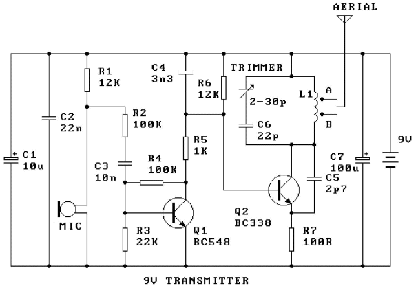
1. You don't need 10u and 100u electrolytics. You don't need any
electrolytics AT ALL.
2. The microphone is heavily turned on via the 12k resistor then its
output is attenuated by the 100k resistor. 12k is too low and will
overload the microphone considerably.
3. The oscillator is DC biased via the first transistor and this
is not a good arrangement. The oscillator should be "self biased."
4. The trimmer capacitor should be in parallel with the 22p so that it
has a small effect on adjusting the frequency.
5. R5 will have almost no effect on the operation of the circuit and is
not needed.
6. BC338 is a power transistor and is not designed for 100MHz operation.
7. The 22n should be across the battery (and not at the audio end of the
circuit) because the function of the 22n is to keep the power rails
"tight" at the oscillator end.
8. The coil is etched on the PC board and this type of coil has a very
low "Q." The circuit will have a very low output.
Overall the circuit is a very poor design and is not worth building.
Here's another absurd circuit from Circuits Today:
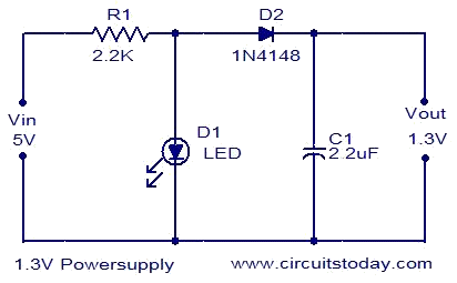
The designer of the circuit claims you will be able to get current from
the output "just like a 1.3v button cell." The LED will take 1.3mA. How
bright will it be????
But look at the 2k2 resistor. For every milliamp that flows though the
2k2, two point two volts will be dropped across the resistor. If 2mA
flows, the voltage at the top of the LED will be 5v - 4.4v = 0.6v. If
you try to draw 3mA, the voltage will be 5v - 6.6v =
?????? Obviously you cannot draw 3mA.
This is a simple lesson. Before you draw any circuit and put it out for
others to see, TEST IT.
Even the simplest circuit can be incorrect.
Circuits Today is an Indian site and they have not replied to any
of my comments. They don't even have an email address. That's the
wonderful part of the web. You can find all sorts of material and you
have to sift through everything to work out if it is correct.
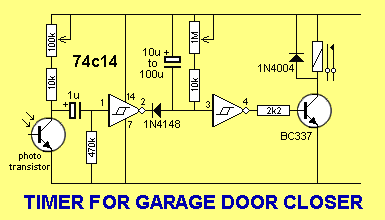
Here's an over-designed circuit from Circuits Today:
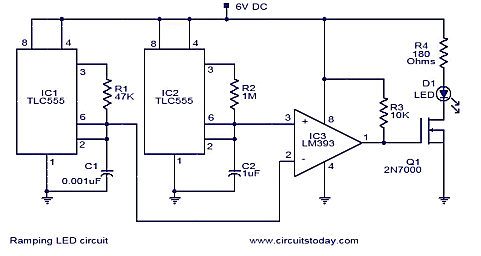
The circuit above can be replaced with the following circuit:
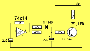
The circuit gradually fades the LED ON and OFF.
Before designing a circuit, DO YOUR HOMEWORK. Look on the web and see
how other's have tackled the task you are working on.
There's always a simpler, cheaper, way to do things and that's why you
need to research things before starting. The 74C14 has six Schmitt
inverters and we have used only one. The 22u charges via the 470k and
discharges via the 47k. This creates a gradual on/off effect that has
equal timing. The unequal charge / discharge rates compensate for the
non-linear surrounding components.
Here's another circuit from Circuits Today: (every circuit they issue each week has a fault!)
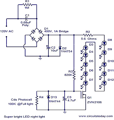
Here's the original circuit:

The bridge in the Circuits Today circuit is incorrect. The zener
values are not identified with the voltage rating and the 5R6 will have
no effect on protecting the LEDs.
The comment about the CdS photocell needs more explanation. The author
states the circuit will turn off when the light falling on the photo
cell causes the resistance of the cell to drop to 100k. At this point in
time, the LEDs are illuminated and the voltage from the rectifier is
approx 36v - due to the voltage drop across the 10 LEDs.
This voltage is prevented from rising above 15v via the zener across the
photocell.
When the resistance of the photocell falls to 100k, the only two
components to consider are the 820k and 100k photocell, in series. This
will produce a voltage at the mid-point of 3.9v This is too high
to turn off the DMOS FET ZVN 2106. You will need to either add a resistor across
the photocell or allow the brightness of the room to increase.
The current taken by the circuit is the same when the LEDs are not
illuminated (the current is taken by the 39v zener) so the addition of
the DMOS FET and zener diodes are not really needed.
Here's what is needed:
Here is a
project from Electronics For You, an Indian publication. The
circuit is over-designed. See if you can work out what the circuit is
trying to do and see if the simplified circuit does the same job:
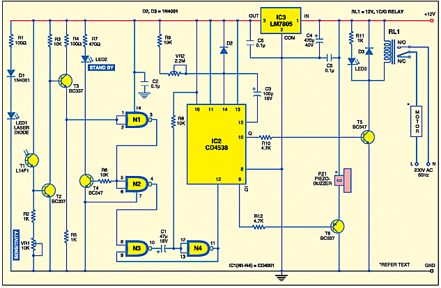
This automatic door opener can be made using readily available
components. The electromagnetic relay at the output of this gadget can
be used to control the DC/AC door-opener motor/solenoid of an
electromechanical door opener assembly, with slight intervention in its
electrical wiring.
A laser diode (LED1) is used here as the light transmitter.
Alternatively, you can use any available laser pointer. The combination
of resistor R1 and diode Dl protects the laser diode from over-current
flow. By varying multi-turn trim-pot VR1, you can adjust the
sensitivity. (Note that ambient light reflections may slightly degrade
the performance of this unit.)
Initially, when the laser beam is falling on photo-transistor T1, it
conducts to reverse-bias transistor T3 and the input to the first gate
(N1) of IC1 (CD4001) is low. The high output at pin 3 of gate N1 forward
biases the LED-driver transistor (T4) and the green standby LED (LED2)
lights up continuously. The rest of the circuit remains in standby
state.
When someone interrupts the laser beam, photo-transistor T1 stops
conducting and transistor T3 becomes forward-biased. This makes the
output of gate N1 go low. Thus LED-driver transistor T4 becomes
reverse-biased and LED2 stops glowing. At the same time, the low output
of gate N1 makes the output of N2 high. Instantly, this high level at
pin 4 of gate N2 triggers the monostable multivibrator built around the
remaining two gates of IC1 (N3 and N4). Values of resistor R8 and
capacitor C1 determine the time period of the monostable.
The second monostable built around IC2 (CD4538) is enabled by the
high-going pulse at its input pin12 through the output of gate N4 of
the first monostable when the laser beam is interrupted. As a result,
relay RL1 energises and the door-opener motor starts operating. LED3
glows to indicate that the door-opener motor is getting the supply. At
the same time, piezo-buzzer PZ1 sounds an alert. Transistor T5, whose
base is connected to Q output (pin 10) of IC2, is used for driving the
relay. Transistor T6, whose base is connected to
Q output of IC2, is
used for driving the intermittent piezo-buzzer. 'On' time of relay RL1
can be adjusted by varying trim-pot VR2. Resistor R9, variable resistor
VR2 and capacitor C3 decide the time period of the second monostable and
through it on time of RL1.
The circuit works off 12V DC power supply. Assemble it on a
general-purpose PCB. After construction, mount the laser diode and the
phototransistor on opposite sides of the doorframe and align them such
that the light beam from the laser diode falls on the phototransistor
directly. The motor connected to the pole of relay contacts is the one
used in electromechanical door-opener assembly. If you want to use a DC
motor, replace mains AC connection with a DC power supply.
The first thing you have to work out is the operation of the CD 4538:
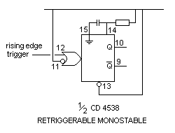
It is wired as a retriggerable monostable and this means
when Q goes HIGH and Q
goes LOW, both the relay and piezo are energised.
The timing of the output is controlled by the 10k stopper resistor and
2M2 pot.
The chip is triggered by a pulse from N4 and N3 and N4 create a short
pulse while the 47u charges via the 10k resistor.
This has been done so the light falling on the photo transistor can
be any length of time but the circuit creates a delay determined by the
4538chip.
All circuitry above can be done with a few gates of a Hex Schmitt Trigger
chip (74c14 - CD 40014 -
CD 40106):
TP-107 Series Surface Mount Tape/Reel Test Points

The profile of the TP-107 readily accepts most
commercially available spring clips and probes while
providing a positive and secure anchor to the SMT board.
Since a test point is subject to mechanical stress, the
strength of its bonding, particularly on a surface mount
design, is crucial. The TP-107 achieves this through a
unique forming process which doubles the surface area of the
test points mounting. This is accomplished by forming the
flat wire design in a spiral wrap on the mounting base
resulting in an adhesion to the solder pad which requires in
excess of 18 pounds of force to dislodge the test point from
its solder pad.
The photo does not really make it clear how the test points are added to
a PC board. The photo should show a PC board containing
surface mount components and include two or more test points.
This request has bee sent to the manufacturer:
Components Corporation We will let you know if we
get a reply.
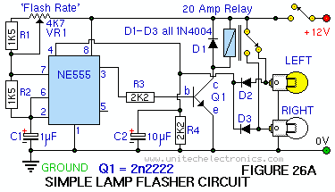
You always learn from some-one else's mistakes and here's another from Circuits Today:
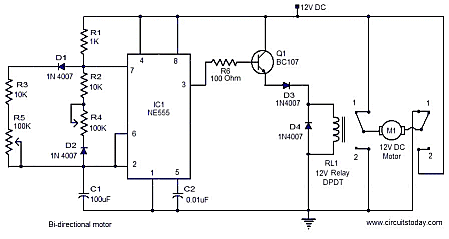
The main problem is the emitter-follower on the output of the 555. The
555 will only rise to about 10v for a 12v supply and the transistor will
drop 0.7v plus the diode will drop a further 0.7v. This means the 12v
relay will only get 8.6v The output transistor should be a
common-emitter stage with 2k2 on the base. Diode D3 is not needed AT
ALL. The diodes need only be 1N4001 1N4002 or 1N4004.
I have tried contacting Circuits Today on 12 occasions
and not had a reply. This is the wonderful part of the web. You
can release information without any experience and without any
accountability. That's why you need to confirm everything you read with
a second and third source.
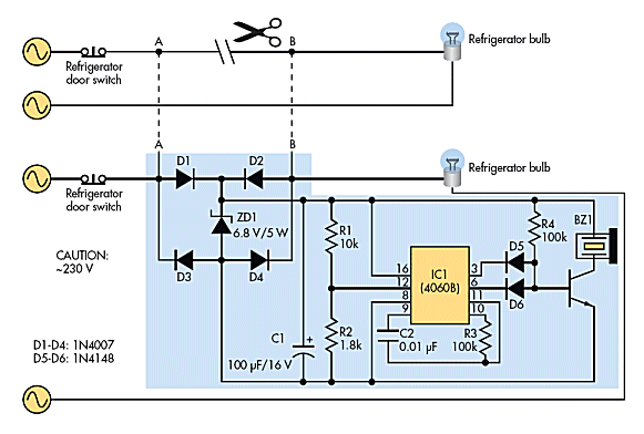
Here's a highly impractical circuit. How are you going
to get at the wiring in a fridge?
Here is a simple circuit that starts to produce a sound about 15
seconds after the Light Dependent Resistor detects light:
Here's another from Circuits Today:
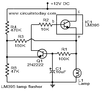
The only problem with the circuit is the fact that it will not work. It
will not start to oscillate. This is easy to see. How does the base of
the 2N2222 get 0.6v to start to turn it on?
The only voltage divider on the base is the 150k and Lamp. The lamp will
be about 20 to 50 ohms. The voltage it will provide is: 50/150,000 x 12
= 0.004V = 4mV!!!!
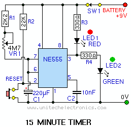
Thus is yet another circuit provided by the Indian website: Circuits Today.
Here's a circuit for you to find the mistakes:
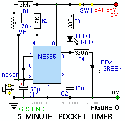
Look at the 150u. What is charging this electrolytic?
It cannot charge via pin 7 as this pin only connects to 0v when
"active." It cannot charge via pin 6 as this pin is an input
to a comparator.
And why connect approx 3Meg across a 12k resistor? And why connect pin 4
to the positive rail via a 12k resistor?
The circuit has now been changed on the website. The 150u
has been changed to 220u ( a value that is available - as 150u is not
available). But it still contains a mistake. It's a very technical
mistake.
Pin 2 detects 1/3 of rail voltage on the capacitor and this pin is being
taken LOW then HIGH via the reset button while resetting the chip via
pin 4. But you cannot control both of these pins AT THE SAME TIME.
You must turn the chip ON by taking pin 4 HIGH, then a few microseconds
later, take pin 2 HIGH. If not, pin 2 will not be recognised. The
easiest solution is to keep pin 4 connected to positive and take pin 2
low via a 22k to start the timing as shown in the following corrected
circuit:
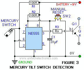
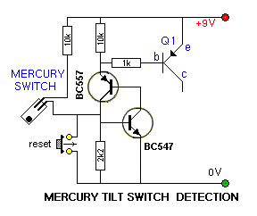
The circuit above is a LATCH CIRCUIT. But it is consuming 10mA while it
is sitting around waiting for the mercury switch to make contact.
By replacing the 555 with two transistors, the circuit will consume zero
current when waiting for the switch to close.
More faults:
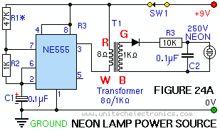
The 555 can only source 200mA and sink 50-100mA at 9v.
The circuit is trying to sink more than 200mA as the 8 ohm primary is an
impedance value at 1kHz and the actual DC resistance will be less than 8
ohms.
The 555 will be overloaded by the output current requirement of the
transformer. But the neon only needs a fraction of a milliamp so
the circuit may work.
More faults:
What is the purpose of the two diodes, 10u, and 2k2 resistor? The
circuit keeps a "HIGH" on pin 4 all the time and these components are
not necessary.
In addition, the 2N2222 can only handle 200mA and the 555 can source
200mA, so the relay can be connected directly between the output of the
chip and 0v rail. The only problem might be the 555 only supplies 10v
when on a 12v rail. It will have to be tested to see if the relay pulls
in.
Here is a misleading pin-out:
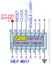
Pin 13 is not a clock line, but CLOCK INHIBIT. When it is HIGH, the chip does not
respond to the clock pulses on pin 14.
Pin 12 is not ENABLE CARRY but simply a "carry out" pin. It
goes LOW at "5" and HIGH at "9." - remembering the first
output is "0."
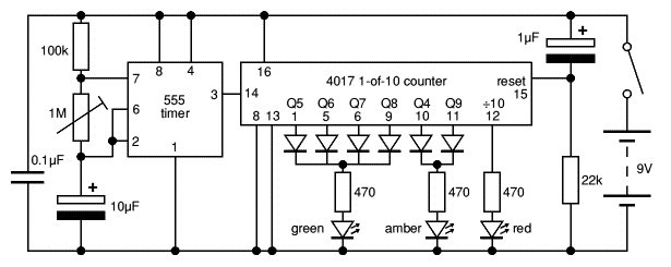
Here is a circuit that uses pin 12 to produce a TRAFFIC LIGHTS project:
Here's another:
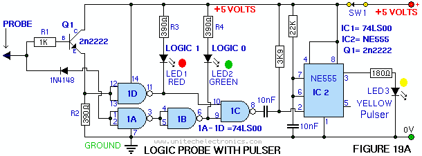
By connecting the LOGIC 0 LED between pin 3 and 0v, you free up one gate
and this will give 2 gates to produce a pulse-circuit and thus you do
not need the 555.
In addition, the circuit is described incorrectly. It should be
HIGH, LOW, PULSE - a Pulser is a circuit that injects
waveforms into a project you are testing.
I should also point out that the Logic Probe is not suitable
for CMOS (high impedance) circuits.
In all the circuits above, one of the things you must do is look
at a circuit and see what is not needed and if it can be done in a
simpler way.
Here's a circuit that doesn't work:
The electret mic does not produce enough voltage to turn on the first
transistor.
See our improved circuit in "200 Transistor Circuits" eBook-2:
CLAP SWITCH. Our circuit also responds to a whistle, tap and clap.
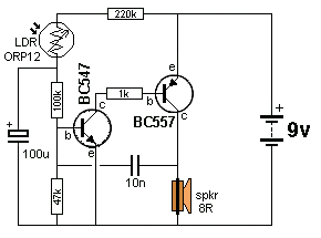
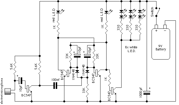
Here's a circuit that doesn't work:
The output from the speaker, when used as a microphone, is only about
20 - 50mV and the pre-amplifier does not provide enough amplitude to
drive the output stage (buffer stage) to produce sufficient volume from
the speaker. The output stage merely takes the amplitude from the
pre-amplifier and increases the current-capability of the waveform about
100 times. In addition, our circuit works with common 8 ohm mini
speakers. It's a great improvement. All it took was one extra stage of
signal amplification (voltage amplification).
The improved circuit can be found in "200 Transistor Circuits" eBook-2:
INTERCOM
The fastest way to learn electronics is to discuss circuits that don't work.
You learn two things. What NOT to do and WHAT to do.
It is very difficult to find a fault yourself and very difficult to see a technical mistake. Mistakes come in many different forms and most electronics enthusiasts don't want to do a lot of reading.
That's why we have explained everything with a circuit diagram.
When designing a circuit, test it by changing some of the components and see if it is "tolerant" of variations and get someone else to put a prototype together.
This topic started with a Key-Hole light that took 14uA when sitting around, instead of less than 1uA. The batteries lasted only a few months instead of a year and the importer went out of business.
A quick look at the circuit diagram would have shown the fault in the design - rather than waiting 3 months to see a load of flat batteries.
Two more points you will learn from this topic are:
1. Don't expect a circuit to work perfectly the first time it is developed. It may need many modifications and improvements. Be ready for this.
2. Don't expect a circuit presented in a book or on the web to work perfectly. It may contain hidden faults - as we have shown.
Page 1
Page 2
Page 3
Page 4
Page 5
Page 6
Page 7
Page 8 ----
Page 10