SPOT
Page 1
Page 2
Page 3
Page 4
Page 5
Page 6
Page 7
Page 8
Page 9 It is pleasing that these pages are read by a number of
visitors who are deeply interested in learning electronics.
Pin 3 of the 555 does not rise higher than 3.5v for a 6v supply. This is one of
the major problems with a 555. This means the PNP transistor will not turn OFF
when pin 3 is HIGH and the circuit WILL NOT WORK.
Car Fuse
THE MISTAKES!
Page 16
Page 10
Page 11
Page 12
Page 13
Page 14
Page 15
Page 17
![]()
You will find the discussions we have presented have never been covered in any
text books and yet this type of analysis is the most important way to learn.
Many of the circuits come from "Electronics Professionals" or "Electronics
Technicians" and yet they contain faults. Most of the faults are due to
inadequate testing but many are due to the fact that the circuit has not
been put together and tested AT ALL.
It is an absolute fallacy to think you can design a circuit and "It will work."
There are many hidden problems such as in-built resistors in transistors,
transistors getting too hot, zener diodes that leak, and the list goes on.
40 years ago I presented a circuit and forgot a component. The circuit did not
work. I vowed I would NEVER present a circuit without building it and
thoroughly testing it. That's the only way to prevent making a FOOL of yourself.
Electronics is wonderful. It PULLS YOU UP. It corrects your mistakes and doesn't
allow faulty circuits to work.
All you have to do is TEST IT.
![]()
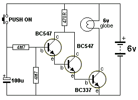
Another untested circuit: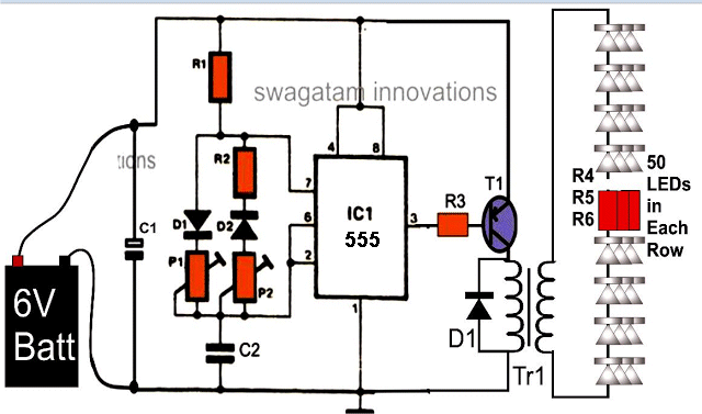
![]()
The BC547 will never turn ON. It is around the wrong way. The base must be 0.7v
higher than the emitter for it to turn on.
![]()
Another untested circuit:
What is the purpose of D3? It serves NO purpose.
The 1k pot does NOTHING. If you turn the pot completely clockwise, the 10v zener
will be across the battery and it will burn out. And the pot will be destroyed.
The pot will never turn the LED off.
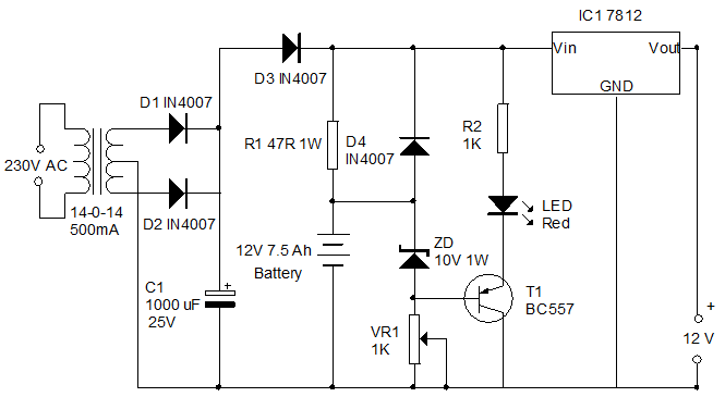
The 14v transformer will produce 14 x 1.4 = 19.6v less 1.4v = 18.2v to
charge a 15.5v battery across a 47R resistor. The current will be 60mA.
Fortunately the transformer will produce about 4 volts more because of the extra
winding on the secondary and the current will be 150mA. Just a trickle charge
for a 7.5Ahr battery.
But the most important fault is the fact that the 7812 will not work when the
power fails. It requires at least 3v above the output voltage for the
electronics inside the chip to provide the output voltage and current. This
circuit has never been tested.
D.Mohankumar has absolutely no idea about
electronics. Here is his rubbish explanation of how the circuit works:
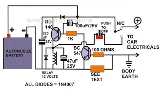
Zener diode ZD and the PNP transistor T1 form the low battery indicator. No
they don't
When the battery voltage is above 11 volts, Zener conducts and keeps the base of
T1 high so that it remains off.
This is NOT true. The transistor is connected as an emitter-follower and it
conducts as soon as the emitter is 0.7v below rail voltage. In other words
it conducts ALL THE TIME in this circuit.
When the battery voltage drops below 11 volts, the Zener turns off and T1
forward biases. LED then lights to indicate the need for battery charging.
This is NOT true. D.Mohankumar has no idea how a
transistor or zener diode works.
![]()
POWER SUPPLY
. Another faulty circuit:
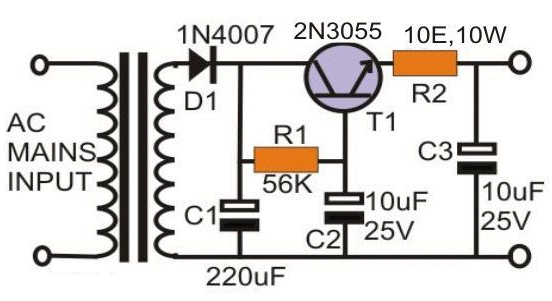
The main fault with the circuit is
the 56k.
When you see a resistor on the base of a transistor, you immediately divide the
resistance on the base by the gain of the transistor and this will be the
approximate resistance of the transistor. It's only a quick way to see if there
is a fault
in the circuit.
The gain of a 2N3055 is a maximum of 70. Using this value we see the transistor
becomes an 800 ohm resistor!!
It will deliver no more than 30mA.
This circuit has never been tested.
![]()
This simple circuit has three faults:
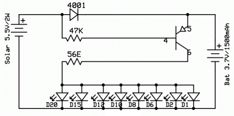
The first fault is the 47k resistor. When the solar panel is not
illuminated, the author of this circuit thinks the 47k resistor will be
connected to the 0v rail.
This is not so. The impedance (resistance) across the terminals of the panel is
an unknown value and measuring a few panels resulted in values from a few kilo
ohms to 100,000 ohms.
During this time the current through the 47k will turn on the transistor and
illuminate the LEDs.
The current though the 47k will be 3.1/47,000 = 0.065mA. If the gain of the
transistor is 200, the collector current will be 13mA. Each LED will receive
less than 2mA.
Although the characteristic voltage for a white LED is 3.5v, they start to
illuminate at about 2.8v and since the circuit will only deliver a very small
current, the LEDs will produce a small amount of illumination.
The circuit is not technically correct as the voltage across a white LED (3.5v)
plus the voltage drop across the transistor (0.2v) leaves no voltage for the
current-limiting resistor (56R).
The author of this circuit is Sebastian Kushero. He refuses to admit there are
any faults with the design.
He replied:
Colin Mitchell has made it his business to denigrate Indian designers. The
circuit provided by us works. If it works that ends the conversation.
Firstly, I was not aware the author was Indian. I just criticized the
faulty circuit, not the designer.
Secondly, to say "the circuit works" is not an engineering reply. It was presented on
a forum and a number of the readers could not get it to work successfully. Sebastian Kushero made no effort to resolve the issue.
The circuit needs 3 changes for the LEDs to produce good illumination. Here are the modifications:
![]()
Before producing even the simplest circuit, you have to know what you are doing.
Here we have a resistive power supply with a 2k @ 10watt resistor on the
front-end. But the resistor will dissipate more than 22 watts.
How do you work out the losses?
The current though the circuit will be = 224/2,100 (230v minus 0.7v
minus 0.7v minus 5.1v) = 0.107 amps.
Power lost in 2k resistor = 0.107 x 0.107 x 2,000 = 22 watts
![]()
Here we have another circuit from electroSome:

The circuits may work, providing the voltage on the collector is 0v when the
first circuit is active and about 5v for the second circuit.
The first circuit shows the transistor is capable of being turned on via the
bridge but it does not show how the voltage on the collector changes. The
circuits are incomplete.
![]()
Here is a circuit from March issue of Electronics For You. Apart from the
fact that the circuit is very complex, the 1k5 base resistor on the output
transistor does not turn the globe ON fully and the transistor gets very hot.
The circuit can be simplified to 3 transistors and 3 resistors. The object of an
electronics magazine is to provide the simplest circuit for the task. Imagine
how annoyed a constructor would be when he finds the same result can be achieved
with less components.
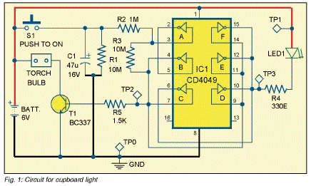
CUPBOARD LIGHT USING TRANSISTORS
![]()
Here's an over-complex circuit:
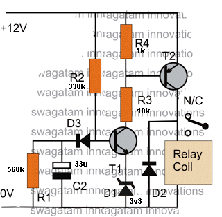
The 3v3 zener, diode D3 and 560k are not needed. Remove the three components and
put a 220k resistor between the 330k and the base of the transistor. The 330k
will charge the 33u and activate the relay. If you want to increase the time,
put the 560k between the base and 0v rail.
![]()
Don't be fooled by a fancy-looking circuit diagram. They can also be filled with mistakes:
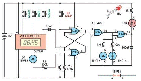
The voltage to pin 6 must be more than 60% for the gate to change state. The two
100k resistors only allow 50% and diode D1 reduces the voltage by 0.6v. The gate
will not change state.
The 10n on pin 5 will not change the state of the gate because output pin 3 will
prevent the change. The 1k on the LED will only allow 1mA.
![]()
RF AMPLIFIER:
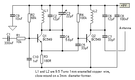
The tuned circuit for the oscillator stage consists of a tank circuit using a
9.5 turn coil and 22p plus 12p capacitor.
The output stage is also a tuned stage and the coil and capacitor must have
approx the same values so the circuit will operate at the frequency being
injected into it via the base. If the output stage does not have a 22p so it can
be tuned to accept the incoming frequency, the output of the transmitter will be
very LOW. 1mm wire is very thick. 0.5mm wire will be more suitable. R3 can be
increased to 470R to prevent overloading the transistor. C7 can be removed. C9
is not needed. R1 is not needed. C1 can be 100n. C8 can be 22n. C4 can be 10p.
![]()
How many mistakes can you get in a simple circuit?
The 1u capacitors are in series and this reduces the current to 35mA.
The 1M resistor is too high. It should be 4k7.
The 10R resistors is not needed. The current through the circuit is limited by
the capacitors on the input and the 10R has no effect.
The transistor can be BC547. The current is just 35mA.
The 1 watt LED will produce very little brightness with 35mA.
![]()

You can see why I always include component values on a circuit diagram.
The circuit above was taken from the web and no other data was available. The
circuit is useless without the component values.
Anyone who produces a circuit without the values on the diagram is NOT an
electronics person.
An "electronics person" can see how a circuit works by looking at the values and
working out what is happening.
NEVER produce a circuit without the values on the circuit. If the parts list is
separate, they can get separated on the web and all your effort is wasted.
![]()
POWER SAVING LED
This circuit was designed by Professor D.Mohankumar and he has absolutely no idea how a zener diode works. This is not the first time he has designed a circuit using a zener diode in the wrong direction.
His ignorant reply to this was: "The circuit works and the discussion is ended." If that's what you get from a Professor who sends his junk circuits to Electronics For You magazine. It's no wonder Indian students cannot learn electronics.
When the circuit turns on, the first 100u electrolytic is charged via the 1k
resistor, emitter-base of the transistor and via the zener diode fitted in the
wrong direction so that it drops 0.6v. That's why the 100u charges very quickly
and the LED comes on at the start.
The 100u stops charging when the voltage reaches about 1.2v from the
supply-voltage as this is the total voltage-drop across the two junctions. At
this point the transistor is still turned on and now the first 100u gets charged
via the 1M and the second 100u gets charged via the 1k and emitter-base of the
transistor. This creates an unknown time-delay because the circuit has not been
put together as a proper time-delay arrangement.
Just because something "works" does not mean it has be designed correctly.
You need to know what you are doing, if you don't want to make a fool of
yourself.
![]()
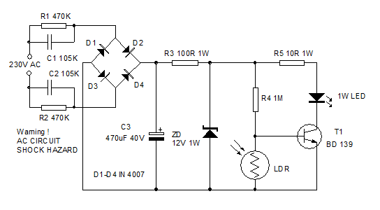
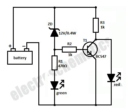
BATTERY SELF DISCHARGE INDICATOR
Here's another one of Professor D.Mohankumar's disasters:
Apart from the fact that the circuit does not work, here is his explanation of how a zener diode works:
The Battery Self discharge Indicator circuit uses only a few components and its
working is simple. A PNP transistor T1 act as a switch to light the LED, if the
battery voltage drops below the safe level. The base bias of T1 is controlled by
a Zener diode ZD. Its rating is 10 volt 1 W. The Zener diodes usually requires
1.6 volts excess than its rated value to enter into the �Avalanche state�.
So, as long as the battery voltage is above 11.6 (10+1.6), Zener conducts and
keeps the base of T1 high. Since T1 is a PNP transistor, it will not conduct
till its base becomes negative. So LED remains dark. When the voltage in the
battery reduces below 11 volts, Zener turns off and the base of T1 becomes
negative. T1 then conducts and LED lights. So the battery can be charged again
to keep it in top condition. Preset VR can be used to set the exact point at
which LED turns on.
Where does he get this rubbish from: "1.6 volts excess than its rated value
to enter into the �Avalanche state�.
If the pot is tuned fully clockwise, the 10v zener will be directly across
the battery and it will be damaged, as well as the 5k pot.
![]()
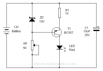
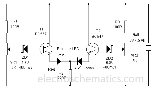
BATTERY INDICATOR
Here's another one of Professor D.Mohankumar's circuits:
The 5k pot will have no effect and is not needed.
The green LED will turn on when the voltage reaches 12v + 0.6v + 2.3v for the
LED = 14.9v This may be too hight for some batteries.
The second transistor is not needed. Here is a simpler circuit:
![]()
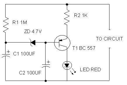
BATTERY CHARGE INDICATOR
Here's another one of Professor D.Mohankumar's circuits:
I wont go through Mohankumar's stupid description of the circuit, because the
circuit doesn't work AT ALL.
Firstly, the 4.7v zener is around the wrong way. It is acting like a diode and
will drop 0.6v.
Secondly, if the 5k pot is turned fully clockwise, it will be damaged as well as
the transistor.
Thirdly, the green LED will never illuminate. It will take 6.8v + 0.6v + 2.3v =
9.7v
Doesn't he check or test ANYTHING?
![]()
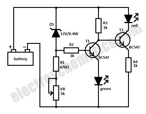
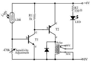
Here's a circuit with a fault we have mentioned before:
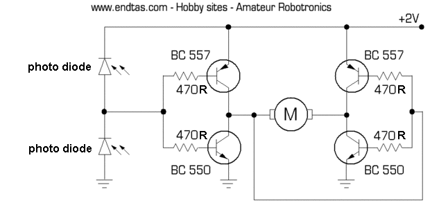
When both photo diodes receive equal illumination, both transistors are turned
on and a short-circuit current flows through the collector-emitter circuits. At
2v supply, this current will not damage the transistors but it is wasteful
current. In addition, the bridge will drop (lose) about 0.5v across each
transistor and the motor will only receive about 1v.
The solution is the following circuit:
It uses a half-bridge to dive a motor in the forward/reverse direction. It does
not have an "OFF" position.
![]()
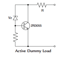
ACTIVE DUMMY LOAD
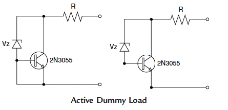
The zener needs a resistor to the 0v rail so it takes a small current and will break-down at the specified voltage. A lightly loading a zener will start to leak at a lower voltage than specified and the circuit will start to work at an unknown voltage-level. The corrected circuit is shown below:
![]()
I have come across another Indian Professor, who is telling his students all
sorts of rubbish.
It is Professor Vidyasagar Sir and his website:
Vidyasagar Sir's Electronics Web
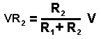
Here is his explanation of the voltage divider:
VR2 = (R2/R1+R2).V
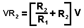
The formulae should be:
He also states:
Also there is only one problem associated with this circuit. This circuit has
very high internal resistance, hence it cannot be used where you require large
current along with the divided voltage�.
This is NOT TRUE.
It should read:
Voltage-divider circuits can be very inefficient, depending on the load. If the
load is turning on and off, the voltage divider circuit is the most inefficient
way to power the load. But if the load is constant, you only need one resistor
and the other resistor is the load.
Of course a voltage divider can be used with a large current and the wattage
lost in the divider will also depend on the voltage being dropped across the
voltage-divider-resistor.
Professor Vidyasagar Sir has replied to me about the formulae. He still
thinks his formulae is correct. Not only does he not understand electronics, but
his mathematics is abysmal too. So far he has refused to change any mistakes on
his site. Wait and see how things will change.
I now find he has corrected his formulae to the following:
VR2 = (R2/(R1+R2)).V
How a "Professor" can make a simple mistake like this is beyond me. And then say
his formulae is correct.
It was not until I explained the mistake in the finest detail and posted the
ambiguity on this website, that the correction was made.
A lot of the other mistakes have magically disappeared from his website. At last
he is learning.
He is still a disaster to behold. I cannot follow him around like "puppy-dog"
and pick up all his mistakes.
He still has a very poor understanding of electronics.
![]()
Here is another total absurdity from Professor Vidyasagar Sir:
He says "the voltage on the base of a transistor can be raised to 3v."
I have made over a million projects (via Talking Electronics Magazine) and have
never experienced a base voltage higher than 0.7v to 0.9v. I don't know where he
gets this rubbish from.
With fundaments like this, It's no wonder Indian students get a shockingly poor
education in their Universities.
Professor Vidyasagar Sir replied to me and said "of course you can raise
the base to 3v. We tried it in our laboratory and it worked."
![]()
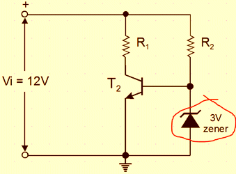
Here's another rubbish circuit from Professor Vidyasagar Sir:
He claims pin 2 will over-ride reset pin 4 and activate the chip !!!
I don't know where he gets this rubbish from. He may have a faulty 555 chip or
pin 3 did not produce a LOW to put the chip into reset, but then he tells the
world that this arrangement WORKS!!
It's a bit like the Pons Fleischmann cold fusion fiasco that turned out to be untrue.
But students are believing this idiot Professor and they will never succeed.
You say I am harsh. But if I was told rubbish like this; and made a fool of
myself later in life, I would be furious.
![]()
Here's another absurd idea from Professor Vidyasagar Sir:
He suggests placing 3 power diodes in series on the 240v line to drop
2.1v so the LED will illuminate.
What an absurd idea. When the voltage reverses, the LED will see more than 300v
and it will BLOW UP !
Vidyasagar Sir is a Professor. Where did he get this
title from??????
Another mistake:
"The element will get only half of the electrical power and thus, its life
increases. Don�t worry about the temperature�! The iron will be equally hot as
it was getting previously."
This is NOT TRUE. The temperature of the tip will be considerably less if
a 400v diode is used. I
have done this with my hot soldering iron to reduce the temperature of the tip and
it works perfectly.
This is another comment from Professor Vidyasagar Sir
without any understanding of what he is talking about. He doesn't understand
thermodynamics, electronics or mathematics. What a disaster.
The 1N4001 diode has a PIV of 50v. The 3-diode combination will provide 150v PIV
and then breakdown, as the voltage rises, so the iron will not get half the
electrical power. Don't forget, the peak voltage of 240v AC is 330v, so 150v
will still allow a high percentage of the waveform to enter the iron.
![]()
Here's a question on a Power Supply test from Professor Vidyasagar Sir:
The question is: What will happen if one diode is reversed:
My answer is: the diodes will be damaged.
Professor Vidyasagar Sir
says this is incorrect.
Of course the diodes will be damaged. The transformer has a short-circuit on the
output and a very large current will flow. Where does he get his understanding
from?????
![]()
Here is an idea from Professor Vidyasagar Sir:
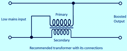
The 240v to 50v @3amp transformer will increase the output voltage when the
mains voltage is low.
He has never tried the circuit because he fails to mention that a 50v
transformer will only produce 40v on the low input voltage (and less current)
and the secondary winding has to be around the correct way to provide boosted
voltage.
The transformer becomes an auto-transformer with an overwind.
You can also use a 240v transformer that has a 220v and 250v tapping.
Connect the 0v and 220v to the "Low Mains Input" and take the output from the 0v
and 250v tapping. This will provide about 20v improvement.
![]()
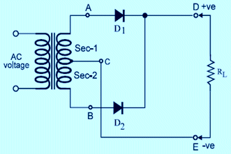
Here is a comparison table for Power Diodes in a power supply from Professor Vidyasagar Sir:
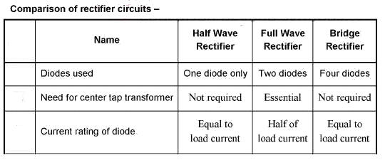
Why is the current rating of two diodes in a centre-tapped power supply only
half the load current?
Each diode is carrying exactly the same current as a single diode in a half-wave
arrangement.
It is absolute madness to derate a power diode in a power supply. Even though a
diode may be carrying current for half the time, you cannot use a diode with a
50% capability. I don't know where
Professor Vidyasagar Sir
gets this false information from.
![]()
Shunt Zener Regulator by Professor Vidyasagar Sir.
It's no wonder Indian students don't understand electronics. Apart from his
terrible English, he has no idea how to explain the operation of a circuit. He
has not explained how the zener diode works and the last two sentences are
gobbledygook:
The zener diode is connected in parallel with load. Hence, it is called as shunt
regulator. When unregulated voltage (Vi) (from a rectifier circuit) is
connected, the current (Is) flows through series resistor (Rs) and the zener
diode operates in breakdown region. So we get Vz = Vo. This voltage remains
constant even though the input voltage changes. The circuit is suitable for
small output current, because the (Rs) is in series with (RL) and so the output
current is less. But series resistor (Rs) protects the zener diode from burning
due to large current.
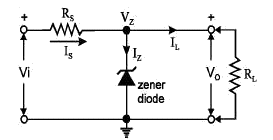
Here is a professional explanation, that I can understand, while using simple
terminology.
We start with the load removed.
The input voltage passes through resistor Rs and the zener diode. When the
voltage across the zener reaches the zener breakdown voltage, current flows
through the zener and the reason why the voltage across the zener does not
increase any further is as follows:
If the voltage across the zener increases, more current will flow through the
zener and this will produce a larger voltage across Rs. This will reduce the
voltage across the zener.
If the input voltage increases, the same reaction will occur and the voltage
will remain stable.
If a load is connected, the voltage across the zener will decrease a very small
amount and the zener will allow a lot less current to flow through it.
If more current is required by the load, it takes the current from the zener.
This can be done until the zener is only passing a few milliamps.
As soon as the zener takes no current, (the current through the load increases
further) the output voltage reduces and the circuit has dropped out of
regulation.
![]()
Here is a question that shows Professor Vidyasagar Sir has no idea how a
zener regulator works, or the fundamentals of mathematics.
A 30v, 600mW zener diode is used for providing a 30v stabilized DC power supply
to a load. If the input voltage is 50v, calculate the series resistance Rs
required for a load resistance of 2k.
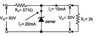
Zmax = 0.02A, VRs = 20v, lL = 0.015A, ls = 0.035A, Rs = 571.43 ohm
The whole idea of a zener regulator is to provide for a fluctuating load. If the
load is fixed, you don't need a zener.
A simple voltage divider can be used.
This is a very bad test question. It does not ask the right questions.
Why have 20mA of wasted current flowing through the zener?
If the current through the load decreases, the zener will be damaged as it is
already taking full current.
But the most disturbing aspect is Professor Vidyasagar Sir's lack of
mathematical understanding.
You cannot provide an answer with a higher degree of accuracy than the supplied
data. He has worked out the resistance to 2 decimal places (571.43 ohm) whereas the data
provided has no decimal places. This is a fundamental mathematical concept and
is just one of the areas where he fails to show competence.
![]()
A high voltage low current regulator power supply is required for an old tape
recorder. The output voltage required is 500v and load current is 15mA. If Vin =
600v and Rs = 5k calculate the power rating of zener diode and current flowing
through it.
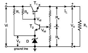
Here is another minor mistake from Professor Vidyasagar Sir
T1 is in series with the load, so it can provide large output current.
If the current through the load decreases, the output voltage will increase. It is quickly adjusted by the circuit and brought to normal value.
The process is as follows: If Vo increases, the voltage across Rb also increases i.e. Vb2 increases. So T2 is more forward biased. Hence, its Vc2 decreases. But Vc2 = Vb1, so Vb1 decreases. Hence, transistor T2 is more reversed biased. So its Vce increases. But Vo = (Vi - Vce) and Vi = constant, hence, Vo decreases proportionally and restores the output back to its original value.
Obviously Professor Vidyasagar Sir means: Hence, transistor T1 is more reversed biased.
Using the terms FORWARD BIASED and REVERSE BIASED makes it very difficult for students to understand the operation of a circuit. As soon as you use terms like this, you turn the students OFF. Maybe this is why no-one has picked up the fault in the description.
He says he gets 5,000 visitors each day from around the world
who hold high
designations in Universities and colleges
and yet no-one has picked up the numerous mistakes in his articles.
Here is another garbled and faulty explanation of how a current-limiting circuit
works by Professor Vidyasagar Sir
Working: here transistor T3 is a silicon transistor along with Tl and T2. So it
requires Vbe > 0.6v for forward biasing. A small resistor Rsc is connected
between base and emitter of T3. Now the load current must flow through T1 and
Rsc only.
Here's another major mistake from Professor Vidyasagar:
This articles is 10 years old and that means over 18 million people have visited
his site and not a single correction has been made. He is obviously saying
that University people don't have a real understanding of electronics either.
![]()
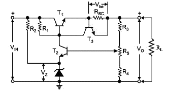
1) Normal condition: When the load current through Rsc is less than a particular
value (i.e. ILmax), which CANNOT produce 0.6V across base-emitter junction of
transistor T3, so it is cutoff. In this condition, transistor T1 and T2 work
normally and the circuit provides regulated output voltage.
2) If load current becomes ILmax: When the load current through Rsc is
sufficient to produce 0.6v across it, T3 is forward biased. So its Vc3 becomes
zero. But Vc3 = Vb1 = 0. Hence, T1 is cutoff. So Vce of T1 becomes equal to Vi.
Hence, Vo = (Vi - Vce) = 0.
Since output voltage Vo is equal to zero, the circuit is almost in dead
condition. The excessive current through T1 thus becomes zero and it is
protected from burning due to excessive heat that may produce in it.
A number of inaccuracies are contained in the above description and here is an
accurate description:
When the load current increases, a point is reached where the voltage across Rsc
is 0.6v and transistor T3 turns ON and the voltage between its collector-emitter
terminals will be very small. The actual value will be determined in a moment.
The condition of T3 turning ON will definitely occur when the output is
short-circuited and the purpose of T3 is to prevent an excessive current flowing
through T1 and damaging it.
T3 will turn ON and pull the base of T1 towards the 0v rail. T1 is an
emitter-follower and the emitter will be 0.7v lower than the base.
The emitter of T1 must be 0.6v higher than the 0v rail, so current will
flow through Rsc and keep T3 turned ON.
This means the base of T1 must be 1.2v above the 0v rail for the transistor to
deliver the current through the sense resistor.
The current through T1 does not become zero, but the DESIGN VALUE. The value of
current for which the circuit is designed to provide full output voltage before
current-limiting starts to operate. You will notice Professor Vidyasagar
Sir misses this point and this makes his description very inaccurate. ![]()
It has more than 3 mistakes and he thinks a Common Collector
arrangement means the collector is Common to the Input and Output and the Input
must be connected to the collector. But the positive rail and 0v rail are
considered
to be "common" as far as a signal is concerned because the impedance (or
resistance)
between the positive and 0v rail is very small (via the power-supply) and thus
the
input is connected to 0v rail and the base. Both the 0v rail and
supply-rail
are considered to be "grounded" as far as a signal is concerned, meaning
they both have zero signal or "ripple" on them.
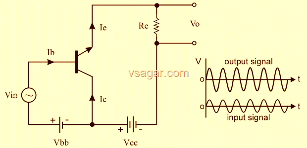
Here is his faulty diagram re-arranged so you can see the mistakes:
Professor Vidyasagar's faulty circuit re-drawn so you can see the faults.
Vbb is around the wrong way.
Vin should be connected to the 0v rail and not "high"
Re should be in the emitter circuit and not in the battery circuit.
Vbb should be connected to 0v rail and base via the Vin voltage source.
When you re-arrange the diagram to follow the conventional way to layout a
circuit, you find it is not a COMMON COLLECTOR configuration. It is some RUBBISH
that Vidyasagar has produced.
That's why I have always said: Draw a circuit in the conventional way so
everyone can instantly see what is happening.
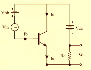
Here is the correct layout:
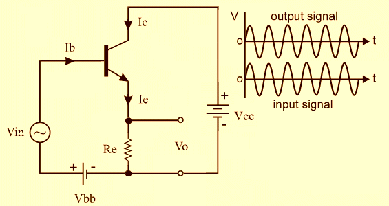
Note: the voltage amplification is almost equal to unity -
the stage does not amplify the voltage - only the current.
You will notice the output voltage is almost the same as the input voltage. In a
Common Collector stage (also called an EMITTER-FOLLOWER STAGE) the output
voltage follows the input voltage (but it is 0.7v below the input voltage) and
is not amplified. Only the current is amplified.
Professor Vidyasagar says the voltage gain is "medium" whereas it
is actually slightly less than 1.
It is obvious Professor Vidyasagar: has no idea what is doing and is a
danger to be on the web. He should remove all his faulty diagrams and
descriptions immediately.
How 18 million previous viewers did not see at least some of these glaring
faults, it beyond me.
The fact is, very few people understand electronics. And when you draw
circuits up-side-down and around the wrong way, you need to be a magician to
rearrange them and see the faults.
![]()
Here's some more muddled paragraphs from Professor Vidyasagar:
Concept of feedback - connecting a fraction of output quantity back to input
of a circuit is called feedback. Feedback is ALWAYS used in amplifier circuits.
There are two types of feedbacks: +ve feedback and -ve feedback.
When feedback is used in inverting amplifier, it is called -ve feedback and when
it is used in non-inverting amplifier it is +ve feedback.
Feedback is NOT always used in amplifier circuits. It is only used to reduce
distortion. He should say: Feedback is almost always used in Audio circuits to
reduce distortion.
A much-better description of feedback is this: Feedback is taken from an output
to a previous stage and if the feedback signal is out-of phase, it is called
negative feedback. The out-of phase signal is designed to correct (or reduce)
any of the highs and lows to reduce distortion. The overall effect is to reduce
the amplitude of the signal.
Positive feedback takes an output signal and adds it to a signal in a previous
stage to INCREASE the amplitude of the signal.
![]()
The more you read Professor Vidyasagar's website, the more stupid it
gets.
He concentrates on forward and reverse biasing of an NPN transistor as
though both these conditions are important.
I understand the concept of forward biasing. It is turning ON a transistor by
supplying voltage to the base.
But I have never reverse biased the base. There is no point in reverse biasing
the base. Simply reducing the base voltage below 0.5v will prevent the
transistor conducting
Professor Vidyasagar's talks about voltages and electrons in the same
paragraph and I find it hard to understand what he is talking about, with his
up-side-down diagrams.
And if his students understand his concepts, they certainly have not passed any
corrections to him about the faulty lecture notes on the website.
Professor Vidyasagar has removed his lecture notes from the side
because other site-holders have copied the notes and presented them as their
own. You can locate these old notes by going to WAYBACK Machine - a
website that archives websites so you can see the content from pervious years.
Vidyasagar Sir's Electronics Web
website:
http://vsagar.com/

[New pages will appear in a new frame.]
Professor Vidyasagar is a teacher and he should not be worried who copies
the notes or what they do with them.
Things started off very cordially with Professor Vidyasagar. He
acknowledged some of the mistakes on this site and said they would be corrected.
But when he realised I had located mistake after mistake, he started to take a
different attitude. He took affront that I had dared to expose his superior
knowledge with mistake after mistake and said many University lecturers had used
his information in their lecturers and no-one else had detected any anomalies.
I am totally impartial as to who produces the faults and you will find the 15
previous pages of Spot The Mistakes come from many different
sources.
But I get particularly annoyed when the holder of a website fails to correct the
mistake on his site.
You will find this applies to people who think they are above correction.
The two most recent examples are: Professor Vidyasagar and Professor
D.Mohankumar.
Neither of them have the faintest idea about electronic design and their
only ability is to regurgitate theory that is already available on the web.
When it comes to providing their own understanding of a circuit, they fail
TOTALLY.
They have done and said some of the most outrageous things I have ever
experienced. But the worst part is: they claim it to be true and pass on their
ignorance to unsuspecting students.
They become a danger on the web and it is fortunate they get a very small
audience.
However even poisoning one student is a tragedy and hopefully these Spot The
Mistakes pages will reach an increasing number of students and make them
aware the web consists of a number of dangerous electronics websites.
It appears that Professor Vidyasagar has now removed his website from the
web. From his initial barrage of comments to me about how stupid I am - "now
I understand you are not just an idiot Australian" to "Now you start drawing
circuits of your own and trying to stick them on my name" to removing some of
the faulty circuits and diagrams and descriptions - to removing his whole site.
If you look at his biography you will find he did only two years of a
preliminary course in electronics and this is the main reason for his total lack
of understanding.
When I first saw his circuits, I did not realise the faulty content because the
word: "Professor" was splashed all over the page. But then I saw 3v on the base
of a transistor. When he replied to my email to say: "of course you can have 3v
on the base of a transistor," I started to realise something was wrong. How
right I was.
It is best to have his whole site vanish, rather than have one incorrect circuit
or statement to poison a student. And that's what has happened.
Some people are going for Monsanto with their criminal GM seeds, I am going for
those who teach faulty electronics. And so far I have won on two accounts.
![]()
After a dozen or more mistakes sent to
Professor Vidyasagar, he got rather irate and started to criticize my
website.
He located this circuit:
http://www.talkingelectronics.com/projects/5v/5v.html
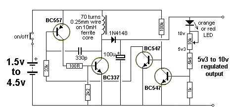
and said "this circuit has never been tested practically, because a regenerative latch between the feedback of BC547 and BC557 will be produced." "Only an idiot can publish such nonsense circuit."
How wrong he is.
Firstly I NEVER put a circuit on my website before it has been built and tested.
(I am not like him with his JUNK, untried, circuits.)
Secondly, the BC547 and BC557 will never feedback and produce "lock-up." The
BC547 simply adjusts the bias on the BC557 (the current flowing in the base
lead) and this has an effect on the frequency of the oscillator, made up of the
BC557 and BC337.
The circuit works quite-well and produces a good (current) output from as little
as 1.5v supply.
See the link above for more details.
All the knowledge of "holes" and "electrons" (for the past 32 years) has not
helped him understand how a circuit works. So, I ask you, why spend years
learning the theory if you want to understand how to design circuits.
Recently, an 18 year-old school student devised an electrical cell and a program
to detect all sorts of diseases in the body. Along with this a girl wrote a
program to analyse X-ray scans to detect cancer cells. The tests are 2,000 times
cheaper than present tests.
Where is their 32 years of theoretical knowledge? They have written programs
that totally supersede anything currently available. Their skills have left the
research scientists in total awe.
I have not had one single sensible comment from
Professor Vidyasagar. From the circuits above, (that he has produced), I
leave it to you to decide if you want a person like him to teach you
electronics.
I certainly don't and if he were my teacher, I would be trying to get him
dismissed.
He is a danger even walking the corridors of a University.
I have never experienced such incompetence before. And such arrogance, telling
me: "Only an idiot can publish such
nonsense circuit." If I
could understand his English, I would tell what he is saying.
![]()
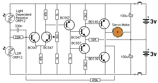
Here's a circuit from works supervised by
Professor Vidyasagar.
The circuit has no current-limiting between the two transistors and if the
LDR turns on with bright light, its resistance can be as low as 300 ohms.
This will allow 2mA to flow in the base of the first transistor and more than
200mA in the collector-emitter circuit. This is obviously wasteful current and
the students are not advised to add a current-limiting resistor to
prevent excessive current-flow.
A very poor demonstration-circuit.
![]()
Here's an absurd description of
Professor Vidyasagar telling a reader how to create
a circuit with a PNP transistor:
"To operate the PNP transistor as a switch, connect a pencil cell across base(+)
and emitter(-) and an LED in series with a resistor of 330ohms, in collector
circuit. connect +ve of another battery of 6V across one terminal of this
resistor and -ve to emitter.
Now when pencil cell is connected the transistor switch is ON, and when the cell
is disconnected, the LED will be OFF."
Here's the faulty circuit:
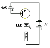
Professor Vidyasagar never tests anything he says. He makes a fool of
himself. The 1.5v cell is around the wrong way and the 6v battery is around the
wrong way.
He gets his faulty understanding of how a transistor works from his theory
article:
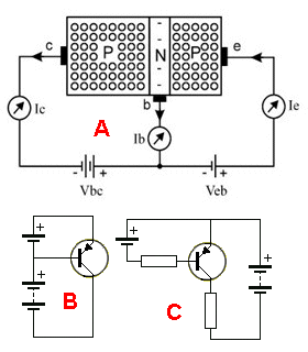
Figure A is a bad representation of biasing
a PNP transistor because the two batteries are "fighting each other"
due to the different currents flowing and there are no current-limiting
resistors to prevent the junctions being destroyed. It has been redrawn in
diagram B to show the faults.
The correct circuit is shows in diagram C.
He states: Personally, I hate PNP transistor, its overall working and even using
it in any of my projects and circuits. This is because, its working is very
difficult to understand.
Here is his photo:

If he doesn't understand how a PNP transistor works, how can he possibly explain
its operation to his students!!
Here is part of his biology:
How can you say you are an expert, when your website is filled with mistakes?
Not only that. You fail to remove the faulty items when they are pointed out to you.
You have absolutely no regard for visitors to your website. You don't even have the decency to make the corrections.
With 3 qualifications in electronics it shows how perfunctory these qualifications are. He cannot even draw a circuit correctly, wire a 555, bias a transistor or correctly analyze one of my circuits.
This makes two electronics professors with exactly the same incompetence.
It proves it is very easy to regurgitate theory to a class of students without having any electronics ability AT ALL. This also proves the fact that it is not necessary to know all the atomic fundaments of the structure of the atom to become an electronics design engineer.
It's wonderful to know the structure of a transistor, but it is not needed. There is a limited amount of time in the day and you need to learn as much as possible to equip yourself for a career in electronics. And that involves knowing how to design and how to fault-find. All the rest is a bonus and can be learnt AFTER the essentials are understood.
Universities have everything around the wrong way. They expect you to be a research-scientist and not a down-to-earth design-engineer.
Up to now, neither has fixed the faults on their website, however Professor D.Mohankumar has given up sending out weekly circuits containing his absurdly faulty, untested designs.
It is hoped Professor Vidyasagar will also cease displaying his ineptitude with electronics. He is just a danger to budding electronics enthusiasts. The latest news is positive. It looks like Professor Vidyasagar has ceased putting his faulty discussions on his website.
This makes 3 website-owners come to grips with the fact that they don't have the capability to inform and assist others in the complex world of electronics.
My campaign goes back over 20 years where I bought text books and made corrections to the text and circuits and sent the copy to the publishers. Fortunately the books were never reprinted.
One visitor emailed me today and asked if the comments on this section had been tried and tested. He says:
Firstly I would like to thank you for your wonderful website , especially the section of Spot the Mistakes and the section on FM transmitters.
I just wanted to confirm one thing. While you are criticizing and finding faults in the various circuits available on the web and in electronics magazines and in most cases giving the rectifications, do you yourself test your suggested changes and try out before putting them on your website ? Or are they just suggestions or try outs?
My reply: I can see if a circuit will work or if it will not work.
I have already mentioned this point before. As you become more capable in the electronics field, you can "SEE" a circuit working in your mind and you can see what is happening. It's a bit like putting a circuit in a simulation package and watching it operate.
This is what I have been doing 20 years before these packages were invented. Although I cannot see the operation of ALL circuits, I concentrate on those I am familiar with and these pages reflect that capability.
However it is most important to have the component values on the diagram. I cannot works with blank values. It is the values that let me know what is happening at each junction of the circuit.
I am not "Mr Magic" I don't make things up. The circuit values produce the results, however I don't put a new circuit on the web without firstly building it and testing it. That's why I know the 3v to 10v power supply circuit above has no faults. It has been built and tested and photographed.
I am not doing this to better my cause. I am doing this to show a completely new way to master electronics.
I already get hundreds of emails from readers who have read my books and magazines over the past 30 years and say my approach changed their life.
My approach works. It doesn't supplant an education but is a precursor or preliminary suggestion, before taking up a course. It's a bit like sharpening your colour pencils before taking art class.
You should have made dozens, if not hundreds of projects before starting a course. To think you are going to learn electronics in a course is like thinking a CRO will show you the fault in a TV.
It just doesn't work like that.
Here's some more stupid things from Professor Vidyasagar's website
:
In forward biasing of NPN transistor its collector base junction is
________ biased.
The collector-base junction is never considered when biasing an NPN transistor.
Rectifier diode
Tunnel diode
Zener diode
Gunn diode
Negative what?????
Resistors R1 and R2 � 470 ohms (if transformer rating is 100mA. However, if it
is 250mA or 500mA, then use strictly a value of 1kohms.)
The current rating of the transformer has nothing to do with the value of R1 and
R2. It does not matter if the transformer produces 100 amps!!! - you can use
470R. How little
Professor Vidyasagar's understands.
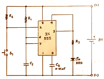
Professor Vidyasagar connected an 8 ohm speaker to the output of a 555
via a 100u electrolytic and created a 1kHz tone. He wondered why the circuit did
not work very well.
The capacitive reactance of the 100u at 1kHz is less than 2 ohms and the 8 ohm
speaker makes an output of 10 ohms. With a supply of 6v, the output current will
be more than the 200mA capability of the chip. (It will theoretically be 4v /10
= 400mA). He then put the chip on 12v !!!
Another dumb thing to do.
Doesn't he know anything about capacitive
reactance??????
Why only 5kiliohm resistors (the three resistors) are used in the internal
circuit of IC555?
What is a kiliohm????
"If the wire is 1 sq. mm. in diameter"
How can you get one square millimeter in diameter????? He means one square
millimeter in area.
He suggests putting a diode in series with your room lights to make them last
longer. The bulbs will be getting only each half cycle of the AC and the
filament will not be as bright. He suggests using a 100 watt in place of a 40
watt to retain the brightness.
But he fails to mention the fact that the bulbs will have a flicker that will be
very annoying.
This is really a silly suggestion.
I could go on all day, trying to worm my way through the poor English on his
website and trying to fathom out what he is trying to say.
I find his site frustrating; imagine an Indian student. He doesn't have a
chance. And yet
Professor Vidyasagar says Indian Universities are the best in the world.
I will leave it to you to decide.
Just go to his site:
http://vsagar.com. It's a "dog breakfast." No index and it's
impossible to find something the second time.
![]()
Here is a circuit of an FM transmitter from: http://www.hobby-hour.com/electronics/wireless_microphone.php
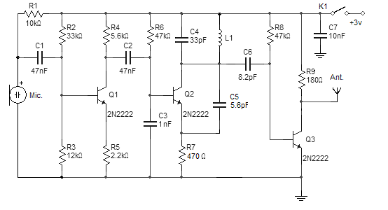
It is pointless having a stage that produces a gain of 2. The first transistor is in a bridge arrangement and the collector resistor and emitter resistor determine the gain of the stage. In this case it is 5.6/2.2 = 2.5!!
![]()
This is a terrible circuit:
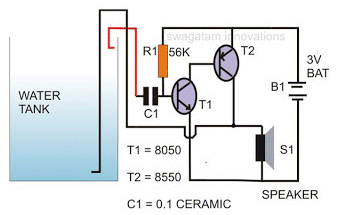
When the water is low, the circuit will not produce a tone but the first
transistor will be turned ON and this will turn ON the second transistor and
produce a constant high current through the speaker.
In addition, this type of circuit will not self-start when the power is already
connected and the water rises.
It needs a "spike" from the power rail to start the oscillating process as the
capacitor must be fully discharged to pull the base low to start the cycle - a
very important point to remember.
![]()
Page 1
Page 2
Page 3
Page 4
Page 5
Page 6
Page 7
Page 8
Page 9
Page 10
Page 11
Page 12
Page 13
Page 14
Page 15
Page 17