SPOT
Page 1
Page 2
Page 3
Page 4
Page 5
Page 6
Page 7
Page 8
Page 9
He has actually described NOTHING.
The first circuit is mine.
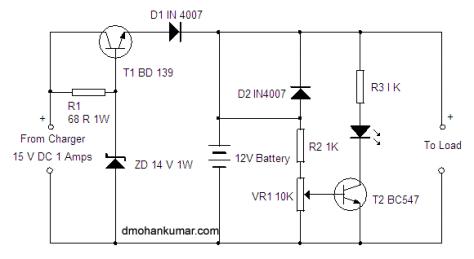
The fault is the 68R - the voltage-dropper to the
18v zener.
Here's another faulty circuit from D.Mohankumar.
Here's another faulty circuit from D.Mohankumar.
D.Mohankumar circuit:
His circuits are ideal to show you how NOT TO DESIGN.
THE MISTAKES!
Page 14
Page 10
Page 11
Page 12
Page 13
Page 15
![]()
These pages have become bigger than I expected.
Although they receive a very small portion of the readership of this site,
they form a very big part of the knowledge-base.
Most text books try to cover the operation of a circuit by using
mathematics. But if you are a beginner, this concept is way over your head.
The whole of Talking Electronics website is designed to talk about circuits
and explain their operation with NO mathematics.
And it has been a huge success.
The readership of the site is increasing every month with over 2,000
visitors each day last year and now it is nearly 6,000 each day.
It is more important to be able to talk about how a circuit works than be
able to solve a mathematical equation.
This fact is highlighted in some of the faulty circuits we have presented on
this page.
Highly educated electronics teachers (in the circuits below) show a total
misunderstanding of how a circuit works and somehow they muddle through a
lecture, leaving the students in a daze of bewilderment.
All they have to do is read through this website and their lectures will
change from absurd to comprehensible.
Until that happens we will be scouring the web for more terrible designs and
add more pages to this ever-increasing file.
You can learn a lot from other peoples mistakes.
I have repaired over 35,000 electronic appliances over a period of 25 years and
most of the problems were due to design-faults.
The most recent task involved a constant-current LED power supply. It
produced an output voltage of 65v and a current of 350mA. You can connect
between 10 and 20 1-watt LEDs to the module.
But the modules were constantly failing.
Two faulty modules and a good module were sent to me for assessment.
On opening them up it was immediately obvious that the soldering to the
leads to the triac were faulty. They had not used enough solder and the
slight heating and cooling of the triac had caused one of the leads to
become "dry-joint."
This was obvious on all three units.
This is a very difficult problem to solve, especially with the new
requirement to use non-leaded solder.
This type of solder is much more prone to cracking and producing dry joints
as the lead in the solder produces a more-flexible joint. When you don't
have lead, you have a very big problem.
The only solution is to open up the modules and re-solder the connections
with a leaded solder and a very hot soldering iron.
This is not allowed under the rules of certification, however the importer
of these modules has no other option - the fail-rate was so high that the
cost of replacing the units at each location was sending him bankrupt. Even
replaced units were failing.
To make the units 100% reliable, I would also solder a very fine strand of tinned
copper wire from the tip of each lead of the triac to an adjacent land on
the PC board. I know this is time-consuming but it works out cheaper than
the cost of a single "call-out".
![]()
Here is a lecture from a "Professor."
Not only is the description vague but he really doesn't know what he is
talking about.
Just when I expected him to describe how the base bias resistors were
selected, he did not provide an answer.
That's because the circuit is much more complex than you think.
Firstly, you have to remember this:
The energy (current) is not passed to the speaker though the transistor but
via the load resistor. The transistor merely discharges the electrolytic
(connected to the speaker) so that it can be charged again via the load
resistor.
This action creates one-half of the energy cycle, but the load-resistor
provides the incoming energy.
To pass energy to the speaker, the load resistor has to be a very low value.
If the speaker is 8R, and the load resistor is 8R, we have a starting point
where the speaker and load resistor are connected directly across the power
rails with the electrolytic between them.
If the load resistor is increased, less current will flow to the speaker.
If the load resistor is 100R, less than 10% of the maximum current will flow
to the speaker.
Now we understand how the energy gets passed to the speaker.
The next point to understand is the value of the base resistors.
To continue this discussion, see:
The Transistor Amplifier
![]()
Here's an example of unnecessary components: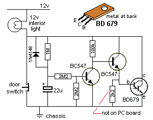
It is a courtesy light extender for cars.
The second circuit is from PC Heaven.
I don't know who designed it, but it has a number of components that are not
needed.
When the door-switch is opened, the 47u is uncharged and it charges via the
globe and base-emitter junction of the T3.
This turns on T2 and T2 turns on T1.
All these transistors turn on but T1 does not fully turn ON as it would
produce a voltage of only about 0.2v across the circuit. It turns ON so that
0.6v is available for the the base-emitter junction of T3 and a little bit
more for C1 so that is starts to charge and pass a current though the
base-emitter junction of T3. The voltage across the circuit is possibly
about 1v.
During this time T4 does not come into operation.
As the 47u charges, the current though the base-emitter junction of T3
reduces and the transistor turns off slightly.
This turns off T2 and T1 a small amount. The voltage across the circuit
increases, and the interior light dims a small amount.
This continues until the voltage across the circuit reaches 11v4 and the
globe goes out. The 33k resistor continues to charge the 47u to 12v and the
voltage across the base-emitter junction of the T3 falls to 0v.
T4 and the 50k pot will reduce the time-delay.
D1 is not needed.
The 50k pot could replace the 33k and T4, and 2 x 2k2 resistors can be
deleted.
This means 5 components are not needed.
![]()
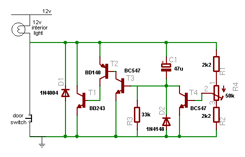
The 18v transformer will produce 18v x 1.4 = 25v and the bridge will drop
2v.
The current through the 68R will be 23 - 18 = 5/68 = 70mA
This current will flow through the zener.
But how much current is required by the 2N3055?
The power supply will only deliver 1 amp max due to the 1N4007 diodes in the
bridge.
The current required by the base of the 2N3055 to deliver 1 amp depends on
the gain of the transistor and a 2N3055 has a low gain. It is a maximum of
70. Using this value, the base current for 1 amp output will be 1,000/70 =
14mA.
This current is taken from the zener, leaving about 56mA.
This is a very wasteful circuit and the zener will be dissipating over 1watt
and getting very hot.
The 68R can be increased to 180R and the zener will not drop out of
regulation.
The circuit has an excess of smoothing.
Normally you require about 1,000u per amp for the first (main) capacitor.
This allows about 50mV ripple.
The 100u across the zener is not needed as the zener provides about 5mV
ripple.
The transistor reduces the ripple by a factor of 70, so the 50mV ripple on
the input is less than 1mV on the output. The 470u on the output reduces the
ripple to less than 1/10th of a mV.
![]()
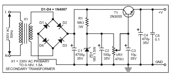
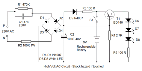
The green LED is supposed to illuminate when the battery reaches
full-charge. But the LED will only turn on when the voltage is above: 12v
for the zener, plus 0.6v for base-emitter voltage plus 2.4v for the green
LED = 15v. The battery never reaches 15v!!
But the biggest mistake with the circuit is trying to charge a 12v battery
from a transformer that is not designed EXACTLY for the job.
You simply cannot connect any transformer to a battery and expect it to
work. That's because a battery is very similar to a zener diode. If you
deliver a slightly higher voltage to either of these devices, a very high
current will flow. That's because the battery is a fixed voltage and the
transformer is (effectively) a fixed voltage and there is no
voltage-dropping component between (such as a resistor). In the circuit
below, the transformer will produce 14 x 1.414 = 19.6v minus 0.7v for the
diode. This means 18.9v will be delivered to a battery that rises to a
maximum of 15v and a very high current will flow.
The transformer will simply overheat and burn out.
Battery-charger transformers are specially wound with the exact number of
secondary-turns to provide a charging -current to suit the rating of the
transformer.
You CANNOT use an "off-the-shelf" transformer.
Why doesn't he test his circuits. He is a Professor at an Indian University,
surely he has plenty of time each day to test everything he produces, instead of
making a fool of himself.
![]()
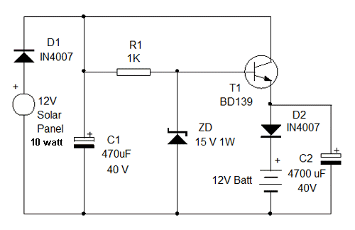
I don't know where he gets his circuits from. But nothing has been tested.
The circuit is supposed to charge a battery when the output of the solar
panel reaches 15v. A 12v panel will be as high as 20v on no-load and in
bright sunlight the panel will reach 16v when delivering a current. Suppose
the battery voltage is 10v (a flat battery). The emitter voltage will be
10.6v.
The base voltage will be 11.2v.
If the panel has an output of 16v, the left side of the 1k base resistor
will be 15.4v and the voltage across this resistor will be 4.2v. This will
allow 4.2mA to flow. If the transistor has a gain of 100, the collector
current will be 420mA.
When the current reaches 500mA, the gain of the transistor falls to between
25 and 70. The only way to get 500mA collector current is to increase the
base current to 500/70 = 7.1mA, but this is not possible as the panel
voltage would need to be 18.3v But as the current-demand from the panel is
increased, the terminal voltage of the panel decreases.
Thus we have a situation where this circuit will not work as expected.
You can see the limiting factor of this circuit is the 1k resistor. It
should be a lower value.
Possibly between 180R and 330R.
The purpose of the 470u and 4700u is unknown. They are not needed. You
don't need to smooth the pulses when charging a battery.
What is the purpose of D1? It is not needed. D2 already prevents the battery
being discharged when the solar panel is not producing a current.
Overall, a very poorly designed circuit.
The transistor will need to be heatsinked as it will get very hot.
![]()
Here is a circuit from
Buildcircuit.com
Resistors R3 and R4 should change places as 330R is far too low as the load
resistor for an electret mic and the base current is too high for the BC547
transistor.
The load resistor for the mic should be 22k to 47k.
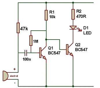
It is not known what effect is trying to be achieved with the circuit but if
the LED is to be illuminated with a clap or whistle, the mic should be
connected to the input of the first stage via a capacitor as shown in the
second circuit. This allows only the AC portion of the signal to enter the
two stages of amplification and illuminate the LED. 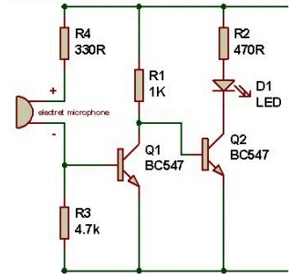
![]()
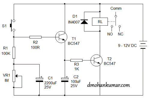
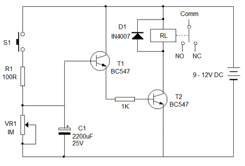
The circuit is a terrible design. When the switch is pressed, C1 is
charged via R1 but since R1 is such a large value, you don't know how long
to press the switch to fully charge the capacitor. C2 will charge quickly
but you don't know how long it will hold the relay closed. There may be a
gap between these two timings. It's just a messy
design.
The circuit can be simplified and improved by removing two components:
![]()
Here's another D.Mohankumar faulty circuit.
Nothing of his is ever tested. He is a danger to students of electronics.
Professors like him (and those from the US on You Tube, don't realise how
ignorant and stupid they are). 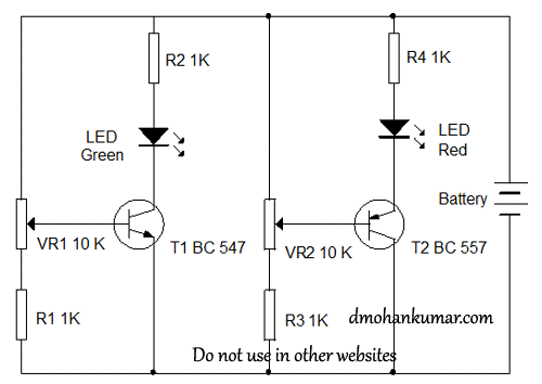
Or you can use two separate LEDs and get the intended effect of the circuit
above.
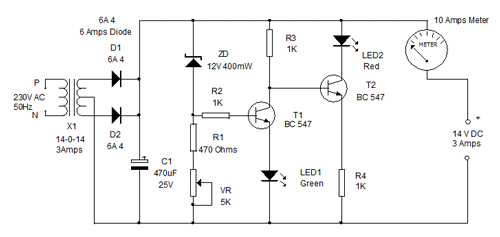
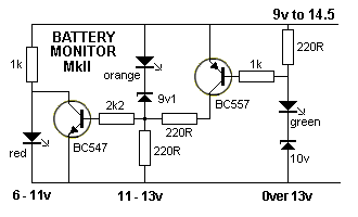
BATTERY MONITOR MkII
This battery monitor circuit uses 3 separate LEDs.
The red LED turns on from 6v to below 11v.
It turns off above 11v and The orange LED illuminates between 11v and 13v.
It turns off above 13v and The green LED illuminates above 13v
![]()
Here is an Infrared LED driver circuit. It has a few mistakes.
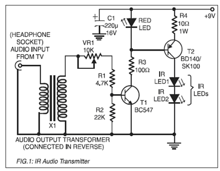
The audio transformer is 8R:1k and the 4k7 on the base of the first
transistor is not needed. R2 is also unnecessary.
R3 will allow 70mA to flow through the red LED if the first transistor turns
on fully. This value should be increased to 330R.
The red LED, in conjunction with T2 and R4 form a constant-current
arrangement to produce a maximum of 100mA through the two Infrared LEDs.
100mA through a 10R resistor dissipates 100mW so a 1watt resistor is not
needed.
T2 passes a maximum of 10mA so a BC547 transistor will be sufficient.
All these little things show the person who designed the circuit did not
know much about designing.
![]()
Here's a faulty circuit from the web. It is a VOICE CHANGER.
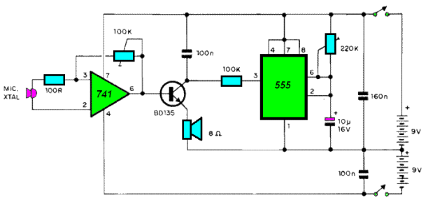
Pin 7 of the 555 is connected to the positive rail. This pin has a
transistor that takes pin7 LOW during each cycle and should be connected to
pins 2 and 6 to discharge the capacitor (10u electrolytic). The chip will be instantly
destroyed if pin7 is connected to the supply.
The 100k on pin 3 will have almost no effect on driving the 8R speaker and
the output of a 741 op-amp is a maximum of 25mA to 40mA.
Xtal Mic's went out of production 25 years ago. They are a very high
impedance device. What is the point in putting 100R in series with a 5 Meg
Xtal Mic?
The circuit obviously has never been tested, it contains so many mistakes.
![]()
Here we go again with another D.Mohankumar faulty circuit.
Here is his comments about the circuit:
This simple circuit gives an LED indication when the 6v
emergency lamp battery enters into the deep discharge
state. As long as the battery voltage is above 4 volts, LED remains off and
it turns on when the battery voltage drops below 4 volts.
When the battery voltage is above 4 volts, the Zener
conducts (the Zener requires around 1 volt excess than its rated voltage for
complete breakdown) and the base of the PNP transistor BC557 remains high
and it will be in the off position. Since T1 is off, LED remains dark . When
the voltage in the battery drops below 4 volts, zener turns off and T1 turns
on and LED lights.
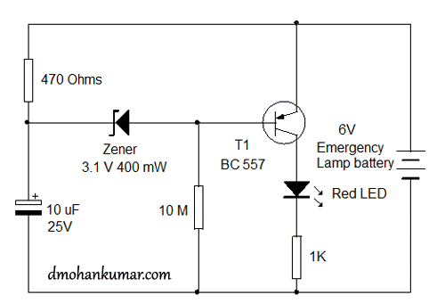
Everything he says is incorrect.
Here is the fault: The zener will allow a voltage of 3v less than rail
voltage to appear on the base of the transistor if you mentally remove
the transistor from the circuit.
But the transistor only needs
0.6v less than rail voltage to turn on.
This means the transistor will be turned on when
the battery voltage is 6v, 5v and 4v. The circuit DOES NOT WORK.
The second problem is the 10M. It is too high. The transistor effectively
amplifies the current through the 10M (6uA) by the gain of the transistor.
Suppose the gain is 300. This means the transistor will allow 6uA x 300 =
1.8mA to flow through the collector-emitter circuit and illuminate the LED.
The LED will not be very bright!
"(the Zener requires around 1
volt excess than its rated voltage for complete breakdown) " - this is
complete rubbish. Don't believe anything Professor D.Mohankumar says.
I don't know where he gets these terrible circuits from. They are certainly
an insight on: "how not to design."
![]()
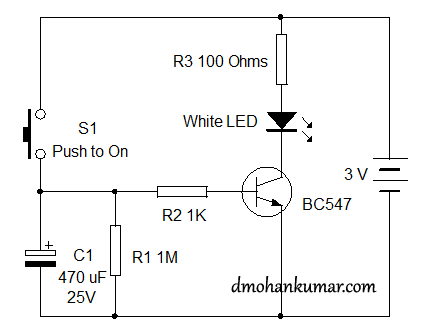
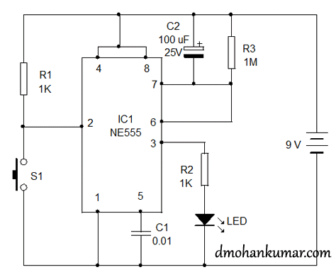
Another D.Mohankumar faulty circuit.
This circuit contains two faults.
The first mistake is technical. The value of the 1k resistor is too low. The
circuit is a timing circuit.
It is a short duration timer which turns on the white LED via the
push-button and after a 1 minute it automatically turns off.
The delay circuit consists of the 470u and 1k resistor. The 1k resistor
should be increased to 10k to produce the longest delay for a 470u
electrolytic.
The second problem with the circuit is the 3v supply. A white LED requires
3.2v to 3.6v for full illumination, however some will work on a voltage
lower than 3v and still produce some output. However it is not wise to
suggest this circuit to beginners as it may fail to operate.
![]()
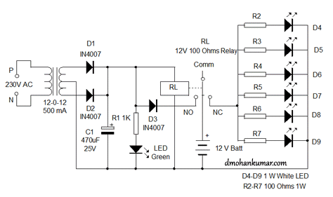
Another D.Mohankumar faulty circuit.
The circuit uses a relay and the battery is being charged when the supply is
present. When the supply fails, the battery illuminates the 6 LEDs.
This circuit contains two faults.
The first mistake is the lack of a current-limiting resistor to the battery.
A 12v transformer will produce over 20v when not loaded and will deliver more
than 500mA to a 12v battery.
In fact it will possibly burn-out.
The white LEDs are claimed to be 1-watt. However one-watt LEDs take 300mA and
100R resistors will only deliver 90mA.
Three LEDs can be placed in series on a 12v supply and this will make the
circuit 300% more efficient.
Just another untested circuit from Professor D.Mohankumar.
![]()
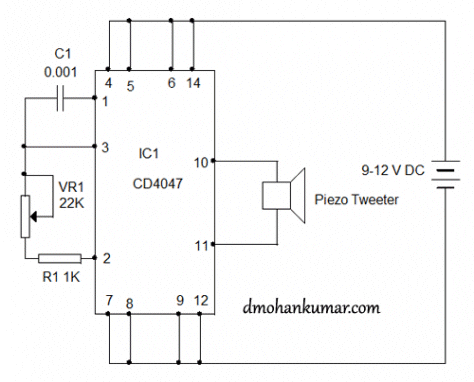
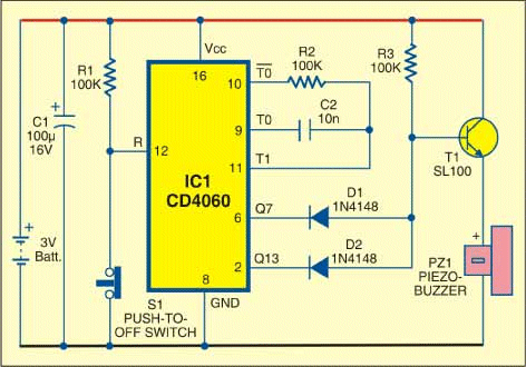
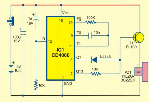
Every circuit Professor D.Mohankumar produces is faulty.
He tests nothing.
Here is an example. The CD4047 chip will only deliver 5 -10mA from the outputs
and the piezo output will be worthless:
![]()
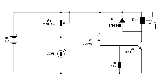
Here's another faulty circuit from the web. It turns ON a relay when light
is NOT detected by the LDR.
But if the 1M pot is turned fully clockwise the two transistors will BLOW
UP.
![]()
Another mistake in the comprehension of electronics from Professor D.Mohankumar
Although the following circuit will work, his understanding of the operation
of the 555 is incorrect.
This is a very good example to help you understand the operation of the 555.
He has the concept of the 555 ALL WRONG.
The time delay in 555 Monostable depends on the values of the timing resistor
connected to its Threshold pin (pin6) and the timing capacitor between pin 6 and
0v rail.. The time taken for charging the capacitor determines the time delay.
Just reverse the connection. The timing capacitor is connected between the positive rail and discharge pin. So the time delay depends on the charging of capacitor. It will take 6-8 times longer than the typical Monostable.
This is totally incorrect.
Placing the capacitor between the positive rail and discharge pin will create exactly the same timing.
The only difference is the capacitor will get DISCHARGED via the timing resistor instead of being charged during the timing cycle.
However the actual level of voltage that will be removed from the capacitor will still be 2/3 of the supply voltage and it will take the same time to remove this amount of energy from the capacitor as it would take to charge the capacitor from 0v to 2/3 of rail voltage.
It takes the same time to discharge a capacitor from fully charged to 1/3 charged as it takes to charge an empty capacitor from 0v to 2/3.
![]()
Another circuit from Professor D.Mohankumar that has not be tested.
The LEDs turn on when the supply fails.
Here are the faults:
1. The circuit will not work because 3 white LEDs need 3.2v to 3.6v each.
2. R3 is not needed. It does nothing.
3.You don't need a BD transistor as the current is only 30mA.
4. The charging current of 30mA is too high for some 9v rechargeable
batteries.
The voltage needed to turn on 3 white LEDs is 3.2v x 3 = 9.6v plus the voltage
drop across the emitter-collector junction of the BD140 transistor (0.2v) =
9.8v.
The voltage drop across the 100R when 30mA flows will be 0.03 x 100 = 3v.
On top of this, a 9v battery will drop to 8.5v very quickly, so it is a very bad
choice.
This circuit will NEVER WORK.
A maximum of 2 white LEDs can be used.
![]()
Another circuit from Professor D.Mohankumar that has not be tested.
Not only will circuit fail to work but if the output of the IC goes LOW, it will
be instantly damaged as the voltage from the regulator will will pass through
the transistor and diode D2 and blow the IC up.
He also says the SCR and zener act as a CROWBAR. They do not. He doesn't
know what he is talking about.
Why is the zener 5watt????
Why is is R5 1watt?????
He claims the circuit is high current. The 7815 is limited to 1 amp. Why
does he use 3 amp diodes in the supply???
The circuit is an absolute disaster.
When will he stop putting this rubbish on the web???
![]()
Here's another absurd circuit from Professor D.Mohankumar
It is a 10amp battery charger.
A transformer to charge a battery is a very special design and the output
voltage is carefully determined by winding the exact number of turns to deliver
the current-capability of the transformer when the battery voltage is low and
the current reduces when the battery voltage reaches 15.5v.
You cannot connect an "off-the-shelf" 10 amp transformer to a battery.
You can think of a battery as a 15.5v zener.
If you deliver a voltage of say 15.6v to a 15.5v zener, it will "take" or "allow
to flow" an infinite amount of current and since the 15v-0v-15v transformer will
deliver over 22v to the battery, an enormous amount of current will flow.
The current will not be limited to 10 amps but it will be exactly like putting a
short-circuit on the output of the transformer and it will deliver so much
current that it will overheat and BURN OUT.
This circuit is an extremely bad design AND MUST NOT BE USED.
Professor D.Mohankumar has absolutely no idea what he is designing.
![]()
Every circuit
Professor D.Mohankumar puts on the web is faulty.
Here is a battery charger:
The output from the BD139 will be 14v - 0.6v = 13.4v
Diode D1 will drop another 0.6v, making the charging voltage 12.8v. This
voltage will NEVER charge a 12v battery.
He claims R1 sets the charging current. This is not true. R1 simply provides
current to the zener to maintain 14v across it.
What is the purpose of D2???? It is connected across a short-circuit !!!!
The circuit DOES NOT WORK.
![]()
Here's another circuit from Professor D.Mohankumar
Protect your LCD TV from over voltage. After a power failure or during
lightening, very high voltage surge develops in the Mains line which is the
major cause that damage TV's. Plasma and LCD TV's are costly devices and use
SMPS type power supplies. The use of a stabilizer is recommended for LCD TV's.
However this low cost circuit can do the job of protection very well. When the
mains voltage increases above 250 volts, it will drop most of the voltage
(around 100 volts) passing through the load and the condition remains as such
till normal voltage level attains.
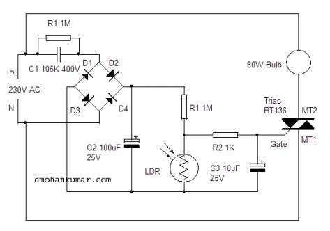
Let's look at the 5k 10 watt resistor.
Here are the facts:
If any device (called a LOAD) is connected in series with a 10 watt resistor, the maximum wattage that can be delivered to the combination is 10 watts.
This is the first fact you have to remember.
The second fact is this: When you connect a LOAD, the wattage delivered to the combination DECREASES.
In other words, if you add a 100watt globe as the load, the wattage delivered to the combination will be less than 10watts TOTAL. The globe will never illuminate.
In fact the total wattage delivered will be 9 watts.
If you add a 1,000 watt radiator as the load, the total wattage will be about 9.9 watts.
The mathematics is very complex but if you add another 5k 10watt resistor, the total wattage will be 5watts delivered to the combination and each will dissipate 2.5watts.
Professor D.Mohankumar's talk about dropping 100 volts depends on the wattage of the load and a 5k 10watt resistor will drop half the supply voltage across it and half across the other 5k 10 watt resistor. But as you can see, the dissipation becomes 2.5watts.
Now you can see how senseless it is to use a 10watt resistor to drop the supply voltage.
The circuit MAY work but it will be very difficult to set the trigger voltage via the 1k and 22k pot.
The circuit is trying to detect 20v increase on 240v and this is 10% change. The 22k pot is wired as a variable resistor and all the adjustment will be at one end of the pot. You will not be able to adjust the pot accurately as the base is tied to the 1k resistor.
The circuit is anther failure of Professor D.Mohankumar.
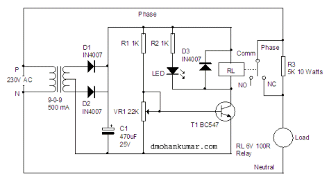
Here's a disastrous circuit from Professor D.Mohankumar
It's an automatic porch light.
The current from the bridge will be about 70mA and
this will appear across the 1M resistor. The voltage from the bridge will be
320v because the 1M will not have any effect in reducing the voltage.
It works like this:
Suppose the 1M is replaced with a 100 ohm resistor placed directly across the
output of the bridge.
The voltage developed across the 100R, (when 70mA is available from the bridge)
will be:
V=IR = 0.07 x 100 = 7 volts.
The load resistor has to be 100 ohms to load a 105 (1u) capacitor-fed power
supply.
If the capacitor is replaced by 100n (104) the load resistor can be increased to
1k and the output voltage will be 7v and the current will be 7mA.
Professor D.Mohankumar has no idea how a capacitor-fed power supply works and he
should not be putting these dangerous circuits on the web. A little knowledge
is a dangerous thing.
![]()
HOW THE CAPACITOR-FED (TRANSFORMERLESS) POWER SUPPLY WORKS
You should also go to our article:
THE POWER SUPPLY Page2, where we cover the capacitor-fed power supply
in more detail.
There have been a number of badly-designed capacitor-fed power supplies on the
web due to a lack of understanding of how they work.
Here is a simple explanation:
Firstly we consider just two components - the feeder capacitor and the bridge.
These will convert the 240v AC to a set of pulses that will have a height (peak)
of about 240 x 1.4 = 330v.
This value is measured from the
The value of the capacitor is not important. The
output will always be the same (330v). The only difference is the current
capability of the output. It will be 7mA for each 100n of the feeder capacitor.
We now add the STORAGE CAPACITOR. This capacitor will remove the "dips" in the
output and produce a voltage that will be close to the peak value.
We now add the LOAD. The load is responsible for producing the output voltage.
This is how it works:
Suppose the load is 1k and the feeder capacitor is 100n. The capacitor will
deliver 7mA and the voltage developed across the 1k resistor will be:
V=IR
V= 0.007 x 1,000 = 7 volts
If the capacitor is 1u, the voltage developed across the 1k load will be 0.07 x
1,000 = 70volts.
One point to note is this: If the load is removed, the output of the power
supply will rise to 330v and blow-up the electrolytic.
In the circuit above, the load is 1M and if you use our mathematical reasoning,
the voltage across it will be 0.07 x 1,000,000 = 70,000volts!!!
Clearly the 1M is out of range to provide any voltage-dropping feature.
The biggest mistake with a capacitor-fed power supply is to think the feeder
capacitor "drops" the voltage. This is not true.
One side of the capacitor see the 240v AC of the "mains."
The voltage on the other side is determined by the current flowing through the
LOAD and the resistance of the load.
The feeder capacitor DOES have an effect on the voltage developed across the
load but thinking the feeder capacitor "drops the mains voltage" will get you
into a lot of trouble.
![]()
Professor D.Mohankumar must be the WORST electronics engineer I have ever come across. Here is another of his untested circuits:
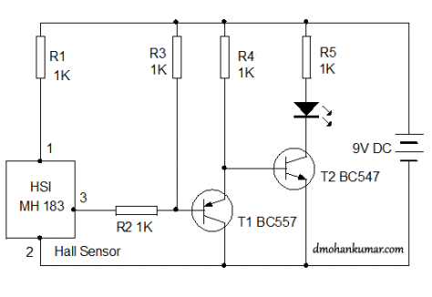
The LED will never go out.
The two 1k resistors on the base of the BC557 will produce half-rail voltage
when the Hall Effect device turns ON.
When it turns ON the output goes LOW and pin 3 will have about 0.2v on it.
If we remove R2, the base of the BC557 will have 0.2v on it when the Hall Effect
device detects a magnetic field.
The emitter will be 0.6v higher than the base and it will have 0.8v on it.
This means the BC547 will see a minimum of 0.8v and the transistor will remain
"active."
This means the circuit will never allow the LED to turn OFF.
Another very badly designed circuit that have never been tested and makes
Professor D.Mohankumar an idiot.
I say this because he has been putting these worthless circuits on the web for
over a year and I have notified him of each and every fault.
Not once has he had the decency to remove the faulty circuit or make any
corrections.
![]()
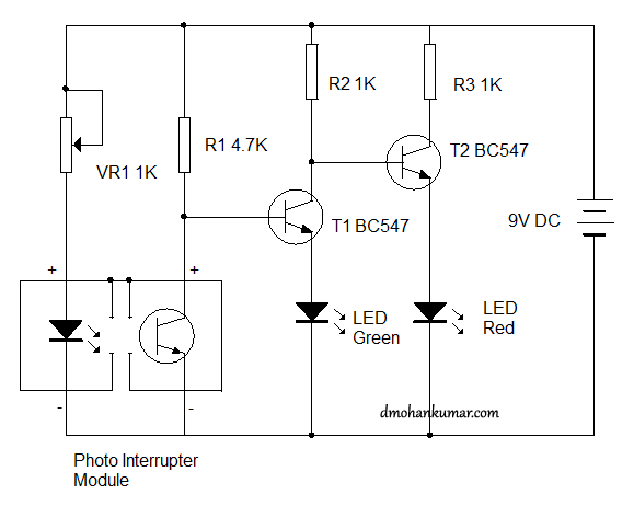
Professor D.Mohankumar is still putting his faulty circuits on the web without
testing them.
This is circuit will not work. The 1k pot will blow up the infrared LED if it is
turned fully clockwise.
And the second fault is the red LED will never go out.
Let's look at why:
When T1 is not conducting, you can consider it is out-of-circuit and T2
illuminates the red LED via R2 pulling the base of the transistor HIGH, turning
on the transistor and the 1k in the collector allows about 7mA to flow and
illuminate the LED.
But when the first transistor turns ON, the green LED will illuminate and it
will produce a characteristic voltage across it of about 2.3v. The voltage
across the collector-emitter junction of T1 will be about 0.2v, making a total
of 2.5v on the base of T2. The emitter of T2 will be 0.6v lower than the base
and it will provide a voltage of 1.9v
The red LED will turn ON when the voltage is above 1.7v and this means the red
LED will always be illuminated.
It's just another badly-designed circuit that should
not be on the web.
![]()
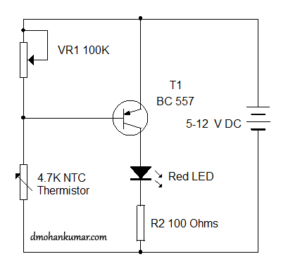
Another untested Professor D.Mohankumar circuit:
The 1M resistor on the base of the transistor will not turn the LED on.
Another untested
Professor D.Mohankumar circuit:
It will be very difficult to adjust the 100k pot to suit the change in
resistance of the NTC thermistor. Just build it and see what I mean.
The 7407 IC is an open-collector device and the outputs will not source any
current. The load must be placed between rail and output. None of the pin
numberings match up with a 7407. The chip-number should be 7408.
Another untested
Professor D.Mohankumar circuit:
This is a GAS sensor circuit. It will not work because the gas
sensor takes 150mA to heat up the sensing chamber. 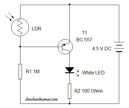
Look at the circuit this way: The 1M resistor will allow 4 microamps to flow
into the base. The transistor will amplify this current 300 times (the gain of
the transistor.) This means the maximum current through the emitter-collector
leads will be 1mA.
It's simple enough to test a circuit before putting it on the web.
Professor D.Mohankumar constantly refuses to test anything before making a fool
of himself.
You can learn a lot from the stupidity of others. ![]()
![]()
Another untested
Professor D.Mohankumar circuit: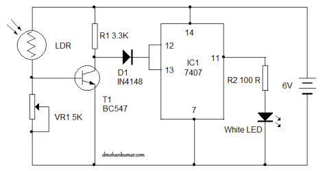
The other problem with the design is the diode on the input to the chip.
This diode will not pull the inputs LOW.
The inputs on this chip float HIGH due to internal resistors on the inputs and
this circuit will not work AT ALL.
It's another failure.
This makes it 100% fail for all the circuits
Professor D.Mohankumar has put on his site in the pasts few months.
It goes to show that you cannot "dream up" a circuit and say it will work. There
are a lot of technical points that must be checked before releasing a circuit.
Simply testing the design is a starting-point.
![]()
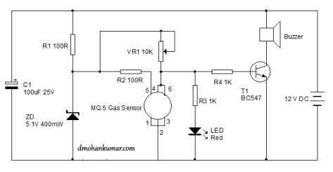
150mA flowing though a 100R resistor will drop V=
The gas sensor will see NO VOLTAGE !!!!!!
This is obviously another untested circuit from a technician who knows nothing
about electronics.
![]()
The faults with this circuit are not obvious until you redraw it using
NAND gates:
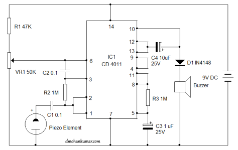
The first problem is the first gate. It produces an oscillator (very similar to
a Schmitt Trigger Oscillator).
(refer to Schmitt Trigger Oscillator section on Talking Electronics website -
see 100 IC projects). The output will always be producing a square-wave waveform
equal to rail voltage and when the piezo is tapped, the waveform will change.
However the circuit is not capable of detecting only a tap on the piezo
diaphragm and thus the circuit will not work.
The 100n in series with the piezo is not needed as the piezo is equivalent to a
capacitor of about 22n.
The next major fault is the lack of a charging-resistor on pins 12/13 to
charge/discharge the 10u. Without this resistor the timing of the circuit is
unknown.
There may be more faults. . . .
The purpose of the 1N4148 diode is unknown.
Build the circuit and prove it DOES NOT WORK.
Another untested circuit from
Professor D.Mohankumar.
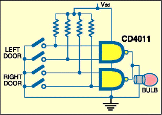
OPEN DOOR ALARM![]()
A little knowledge is dangerous
thing.
![]()
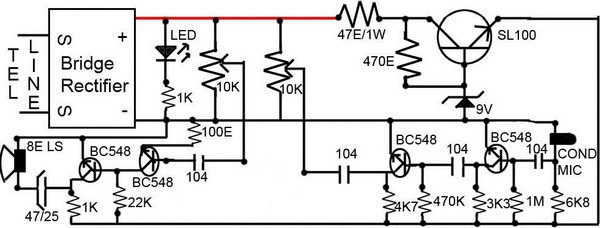
Loudspeaker Circuit For
Telephone
This circuit is a handsfree telephone receiver system. It doesn�t have a dialing
circuit so it�s not a total phone replacement circuit, but it�s a loudspeaker
system (i.e, phone receiver).
Apart from the fact that the circuit drawn up-side-down, some of the components
are not required. The circuit has not been tested but since it comes from India,
you can be sure it will be a very poor performer.
However it is the concept of connecting items to the phone line that I want to
address.
The phone line is not like a normal 50v power supply.
It has very little current capability.
When a 1k resistor is placed on the line, the voltage drops to 22v. With 470R
the voltage drops to 12v.
As you can see, the circuit has a number of resistor across the phone line: 1k
plus LED, 10k, 10k, 6k8, 3k3, 4k7, 22k and 1k.
The combined value of all these is less than 470R and the voltage will drop to
about 10v. This means the the SL100 transistor, 9v zener and accompanying
resistors are not needed.
The base of the first audio stage (the section that drives the speaker) does not have a bias
resistor and this will produce poor results.
Because there is no 100u electrolytic on the power rail of the audio stage, it
is difficult to know how the amplifier will drive a low impedance speaker.
The 1k load on the output transistor will only allow 9mA to flow through the
speaker.
Here is the corrected version with the circuit, drawn so it can be understood.
The circuit has not been tested and may suffer from motor-boating and/or
feedback problems: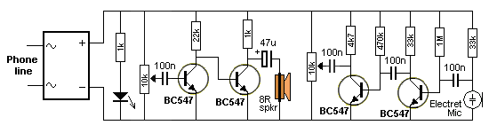
![]()
This circuit beeps if a door is left open for more than a few seconds.
It is one of the worst designs I have seen from India.
The circuit is consuming current when doing nothing and the battery will last
only a few months.
A better design is to place the switch on the supply so the circuit is not
consuming current when it is not activated.
The other change shows how to correctly use the outputs of the chip to activate
the piezo buzzer.
The door pushes the switch open when the door is closed and the circuit consumes
no current.
IMPROVED CIRCUIT FOR DOOR ALARM
![]()
A reader on an electronics forum thought the resistor and capacitor in the following circuit created a TIME CONSTANT.
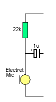
The resistor and capacitor in the circuit above DO NOT act as a TIME CONSTANT. A
time constant arrangement must not have a LOAD connected to the join of the two
components.
At the join of the two components in a time constant CIRCUIT, is a DETECTING
circuit that must not load the circuit AT ALL. The detecting circuit detects
when a certain voltage has been reached and if it puts a load on the circuit,
the timing will be altered.
In the circuit above, the 22k allows the electret mic to take about 0.5mA. This
is the ideal current for the FET inside the microphone. If the current is
increased, the microphone will become more sensitive but some microphones will
start to produce background noise similar to frying bacon and eggs. The 1u
on the output of the circuit allows very low frequencies to the transferred from
the microphone to the next stage of amplification.
![]()
TTL LOGIC PROBE
Apart from the fact that the following circuit will not work until the 15k resistor is replaced with a 1k5, it contains a number of unnecessary components and a difficult to obtain 76k resistor.
The HIGH LED should be red and the LOW LED should be green.
But the biggest mistake is the complexity of the circuit.
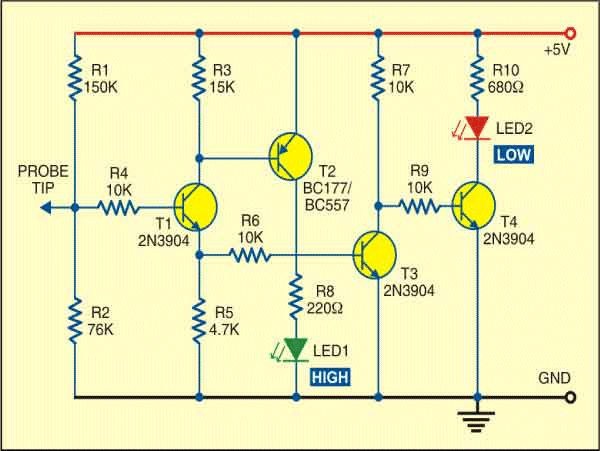
It can be simplified to:
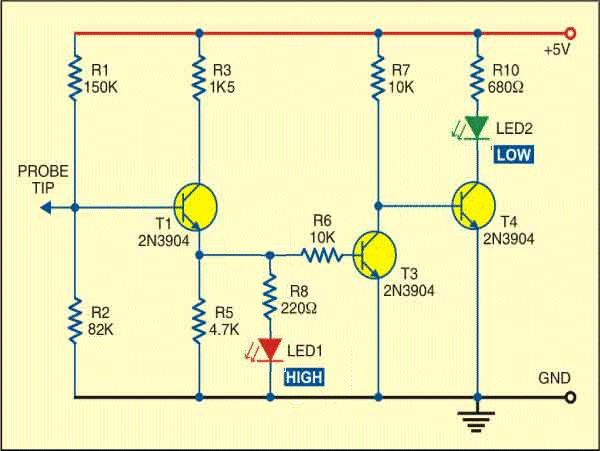
But if you want the simplest circuit, here is the answer:
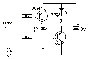
![]()
Here are some glaring mistakes from a recent issue of Electronics For You
magazine, an Indian publication reaching 40,000 or more electronics hobbyists.
The author has used TTL concepts with CMOS technology.
TTL Chips were the first to be developed and the inputs required a small current
to activate the gate. To deliver this current, the associated input resistors
needed to be about 4k7.
CMOS devices were then developed and the input current was less than a microamp.
Input resistors could be as high as 1M to 4M7. The corresponding
capacitor-values for oscillator circuits changed from 470u to 100n to 10u.
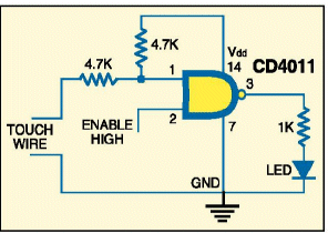
In the circuit above, the resistance of a finger across the touch wires
will NEVER change the state of the gate. The 4k7 resistors must be increased to
470k to 4M7.
The reason is this: Your finger represents a resistance of about 100k. Your
finger and the top 4k7 creates a voltage divider for input pin 1. The gate will
change when the voltage on the input is slightly less than half-rail-voltage.
You will never be able to press hard enough to create a resistance of 4k7.
That's why the resistor must be 100k or higher.
It is not clear what the circuit is trying to do as the enable line
of the gate is floating. The chip will pick up hum from this wire and make the
LED flicker.
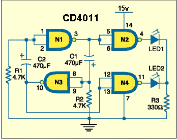
The resistors in the circuit above should be increased to 470k and the
capacitors can be decreased to 100n to 10u. This shows you know what you
are doing and understand CMOS designs.
Another fault is the
connection of the LEDs to a common current-limiting resistor. This allows a
reverse voltage to appear on the non-illuminated LED and the 15v supply may
damage the LEDs. Most LEDs will only tolerate 7v reverse voltage.
The outputs of gates must NEVER be tied together like this as they will be
"fighting each other."
The chip can only deliver 10mA and will not be able to illuminate a globe.
![]()
Look at this PC board from an Indian magazine:
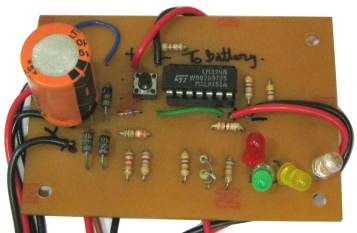
It's a perfect example of how NOT TO DESIGN A PC BOARD.
The LEDs are bent over each other.
The leads are connected to all parts of the board.
The push button is in the centre of the board.
One lead is UNDER the electrolytic.
No overlay. Hand-written words on the board.
Resistors joined together.
This is a kit sold by one of India's leading hobby magazines!
![]()
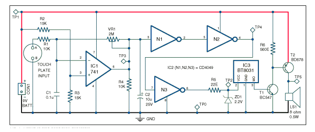
DING DONG DOORBELL
Apart from the fact that the circuit is overly-complex and contains difficult-to-obtain components, it also has a major fault. I am not suggesting you build it, as the Ding Dong chip BT8031-02 is difficult to get.
This is just a study in "HOW NOT TO DESIGN A CIRCUIT."
The CD4049 contains 6 identical gates and one of them could be used in place of the 741 op-amp.
The BT8031 is a melody chip and the exact number for Ding Dong is BT8031-02. This chip will operate from 2v to 5v and the 2.2v zener could be replaced by two red LEDs.
The major fault is the connection of the collector of the BC547 to the base of the BD678 Darlington transistor.
When the BC547 transistor turns ON, the collector is effectively connected to the positive rail via two junctions in the BD678.
If the base receives 0.5mA from the melody chip, the collector-emitter current will be 100mA, if the gain of the transistor is 200. If the gain is higher and the base receives more current, the flow could exceed the rating of the transistor.
It is simply a bad design to connect the two transistors like this.
The base of the BD678 only needs a current of about 0.5mA to drive the speaker and the additional current-flow is WASTED CURRENT.
A BD679 (NPN Darlington) could be used to replace both the BC547 and BD678.
![]()
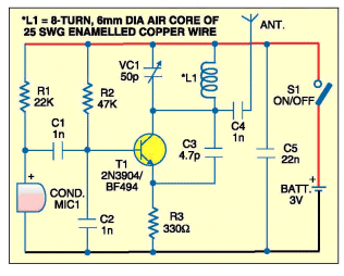
FM BUG
Here is a circuit from a recent Indian
Magazine. It's an FM Bug, and although the circuit looks to be correct, there
are a number of underlying faults.
The major fault is the poor operation of the circuit. A single transistor deign
does not provide enough audio amplification to allow the bug to pick up faint
conversation. It' sonly good for a hand-held microphone where you are talking
directly into the microphone.
But the major fault is the 1n on he output of the microphone. The capacitive
reactance of this at say 500Hz will be about 200k. Very little of the signal
developed by the microphone will be delivered to the oscillator.
The only other problem is the 4p7 feedback capacitor. At 3v, some transistor
will fail to oscillator and the capacitor needs to be 10p.
The 1n on the antenna serves no purpose and the 50p air trimmer should be a
lower value and have a fixed 39p across the coil. An air trimmer drifts a lot
more than a capacitor and that's why it should be kept as small as possible.
See the article:
Spy Circuits for
information on how to correctly design FM transmitters.
![]()
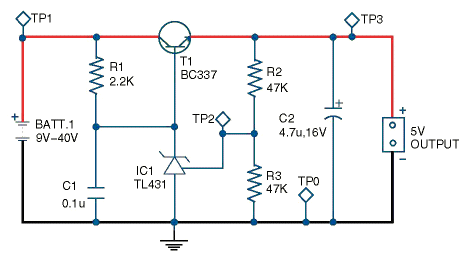
5v Regulator
There is nothing wrong with the
circuit, but the text has faults:
When the reference voltage of IC1 reaches 2.5 volts, its cathode
sinks, (
Working of the circuit is simple. It provides constant 5V output from an unregulated 9-40V DC input. The input power can be from a DC adaptor or a 9V/12V/24V external battery.
The writer obviously does not know what he is talking about. The output of the BC337 never "drops." The voltage simply rises and never increases above 5v. Here is what is call a "slow-motion" description to show how everything works - the "write" has the completely wrong approach:
Suppose the input voltage rises from 0v to 9v.
This will make the discussion easy.
As the voltage rises on the circuit, the transistor passes this voltage to the 4u7 electrolytic. Resistors R2 and R3 form a voltage divider and when the voltage at their join reaches 2.5v, IC1 turns ON and the voltage on the cathode is not allowed to rise any further.
The voltage on the cathode happens to be 5.6v in this circuit and this makes the output of the BC338 5v.
The voltage across R1 will be 9v minus 5.6v = 3.4v The current through the 2k2 resistor will be 1.55mA. This is clearly not microamp current. The author never bothered to test the circuit.
The IC can be replaced with an ordinary 5v6 zener diode. A zener is easier to get and cheaper.
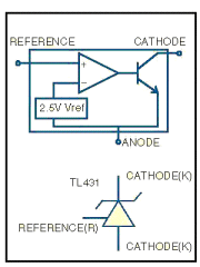
You will notice the pinout of the TL431 shows cathode for both leads. This is obviously a mistake.
The transistor is called a PASS TRANSISTOR. The IC is called a SHUNT REGULATOR.
The theoretical maximum current for this circuit is about 200 times more than the base current. (If we assume the gain of the transistor is 200).
If the base current is 1.5mA, the max output current will be 300mA. The voltage across the transistor will be about 4v and the losses will be 1,200mW. The transistor will have to heatsinked as it can only dissipate about 500mW.
If the input is unregulated, the circuit will reduce the ripple by a factor of 200. You can even use a string of LEDs to create the 5v zener.
![]()
Here's an over-designed circuit.
You don't need a smoothed, regulated circuit to charge a battery. In fact pulsed
current works best as it dislodges the built-up sulphate deposits on the plates.
The output of the regulator is 9.1 - 0.7 = 8.4v The battery will generate
a "floating charge of 7.5v The current through the 33R resistor will be
27mA.
There is NO SKILL in over-designing a circuit. The skill is to produce a simple
circuit. I have already mentioned a number of products that have been simplified
over the years and this represents REAL SKILL. The second circuit does the same
thing with a lot less parts. Generally, when the electricity "goes out" you will
want the emergency light to come on, whether it is day or night as the light
will be placed in a fairly dark location. The LDR feature is not needed.
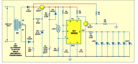
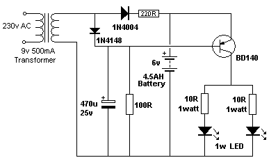
This circuit will illuminate two 1watt High-bright LEDs when the power fails.
The charging current is about 20-30mA. It will take about 7 days to charge the
battery and this will allow illumination for 5 hours, once per week.
A charging current more than 150mA will gradually "dry-out" the battery and
shorten its life.
If the project is used more than 5 hours per week, the charging current can be
increased.
The 220R charging resistor can be reduced to 150R or 100R (1watt). A 4.5AHr
battery can be theoretically constantly charged at 450mA without it generating
excessive gasses via the safety plugs. But any more than 150mA (when the battery
is fully charged) will electrolyise the water (turn it into H2 and O2)
and dry the battery out.
Page 11
Page 2
Page 3
Page 4
Page 5
Page 6
Page 7
Page 8
Page 9
Page 10
Page 11
Page 12
Page 13
Page 15
