SPOT
Page 1
Page 2
Page 3
Page 4
Page 5
Page 6
Page 7
Page 8
Page 9 The whole purpose of Talking Electronics website is to
The capacitor on pin 5 of the 555 is needed to keep the oscillations of the chip
reliable. In this circuit we are requiring unreliability so the 10n capacitor is
not needed.
Here we have a CMOS/TTL LOGIC PROBE from the Laboratories of
Electronics For You Magazine:
We start the discussion with Inverter N3. This is commonly called an Inverter
or NOT-gate.
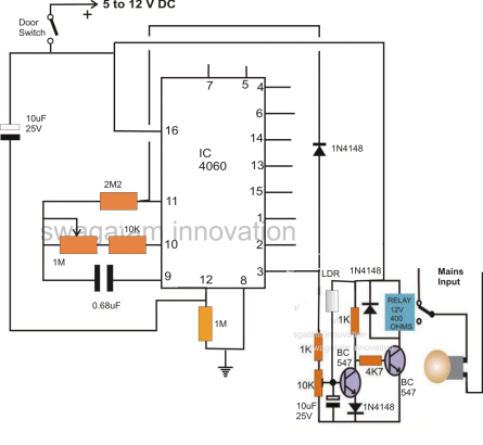
DING DONG DOORBELL
The inputs to the NOT-gates are high impedance and the TOUCH
PLATE could be connected to one of the inverters (NOT-gates) and this would
eliminate the need for the 741 op-amp.
The circuit has been designed to discharge the delay capacitor
when the circuit is turned off. This is a very unusual way to design, however if
the connections to the gates of T1 and T2 are reversed, the discharging
components will turn ON for a brief period and discharge the electro before the
timing begins. A low-value resistor will need to be added in series with the
2,200 to generate the required time-delay.
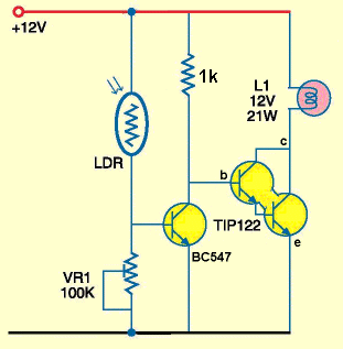
All that is required is two transistors:
The Darlington transistor provides a gain of more than 10,000
and the 1k resistor on the base will turn the TIP122 on hard enough to
illuminate the 21watt globe. Don't forget, the globe will require 5 or
more amps to start glowing as the resistance of the filament is very low when
the lamp is cold and that's why it takes up to 6 times more current.
Here's another over-designed circuit with mistakes:
1. What is the purpose of D3? It is not needed. The
battery cannot feed-back into the power supply as diodes D1 and D2 will block
the voltage.
I put the circuit on an electronics forum and got a number readers detecting
some of the faults. But none saw the circuit as a whole by identifying all the
faults.
You have not identified a single fault.
Using a 1N4007 instead of a 1N4001 is very common - the 1N4007is often the same
price and sometimes cheaper. 1N4001's can be hard to find at times and really
only exists for historical reasons that are now irrelevant.
I pointed out 10 mistakes in the above circuit and got a reply
from D.Mohankumar:
I then said I would analyse circuits before publication in Electronics For You
because so many of the circuits had faults and this was giving faulty
information to newcomers to electronics.
Here's another circuit with a couple of mistakes. You can see who
designed the circuit as it looks just like some of the previous circuits we have
looked at:
If the 10k pot is turned fully clockwise, photo-transistor T1 will
blow up.
Here's another D.Mohankumar circuit. None of his circuits
work. You must not build them.
Transistor T2 will never turn off. The voltage across diode
D1 is 0.7v. The voltage across the collector-emitter of T1 is 0.2v.
This is 0.9v. The voltage on the base of T2 must be less than 0.6v to turn it
OFF.
You cannot get a 7805 to work from the output of a 7806. A 7805 requires 8v
input.
Here's another D.Mohankumar circuit. It is a battery charger:
Connecting a slightly flat battery to the circuit will blow up the LED. When the
circuit is redrawn, you can see why:
There is a direct connection between the 15v supply and the 12v battery, via a
diode-drop of 0.7v which is the base-emitter junction of the transistor. There
is no current-limiting resistor and the LED will blow up.
Here's another D.Mohankumar circuit. It is an emergency lamp:
A 1watt LED takes 300mA. The voltage drop across a 100R when 300mA
flows is 33v!! The 100R can only deliver 25mA.
Here's another D.Mohankumar circuit. It is a battery charger:
The circuit is supposed to turn the current off when the battery reaches 13.5v.
But the "turn-off" circuit consists of an 8v2 zener, the base-emitter junction
of T1 and the voltage drop across a red LED. This is 8v2 + 0.7v + 1.7v =
10.6v The zener needs to be 11v.
This circuit toggles the relay each time the switch is pressed.
Pressing S1 will blow up transistor T1. A 4k7 resistor should be connected in
series with S1.
Here's another circuit from Electronics For You. It has not been
checked by a qualified design-engineer. The circuit possibly works but when you
find out how it operates, you will be HORRIFIED.
It is absolutely essential to draw a circuit so it is instantly
understandable.
You can see the 3v supply goes through the emitter-base junction
of the 3rd transistor and collector-emitter junction of the second transistor,
without any current-limiting resistor.
Here's another disaster from
Electronics For You magazine.
Here's the circuit with corrections and simplified:
A 6v battery must be charged from a supply that is no more than 6.8v.
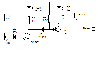
FIRE ALARM
Here's another D.Mohankumar faulty circuit. It is a solar battery charger:
Here is a reply from a reader:
I assembled the Solar Charger circuit as per your design. The solar panel when not connected in circuit shows
22.5VDC. But when I connect it in the circuit the output shows 0.79VDC.
D.Mohankumar could not answer the question.
SOUND SWITCH
There are a couple of technical faults with the circuit:
Remove the transistors and the circuit will work
exactly the same as before:
Here we have a circuit from
Swagatam Majumdar.
It has a number of faults:
I have only identified the resistors as this is where the faults are located.
Here's another untested circuit from
Swagatam Majumdar:
The voltage on the collector of the first transistor will be 0.7v plus 0.2v
= 0.9v when the transistor is conducting and this will not turn off the second
transistor. The diode must be removed. It serves NO purpose. He adds a diode to
the emitter in all his circuits and this is completely unnecessary and creates
faults circuits. He claims to be an "electronics engineer" and yet most of his
circuits have not been tested and DO NOT WORK.
Here's another untested circuit from
Swagatam Majumdar.
The voltage on the collector of the PNP transistor is about 12v. The voltage on
the supply-rail of the 4017 is 5v.
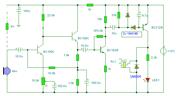
Another circuit from
Swagatam Majumdar with a few minor mistakes. The circuit detects when a car
is hit or bumped and sounds the horn for a short period of time.
The 2k7 load resistor for the microphone is too low. It should be 47k or higher.
You only want to detect a strong hit or bump.
Here we have a capacitor-fed power supply with a slow turn-on feature:
When the voltage is applied, the output of the bridge is effectively 330v with a
current of 70mA. The 330v will be directly across the first 10k resistor and it
will start to charge the 470u. The voltage will then pass through the second 10k
and start to charge the second 470u.
Here's another untested circuit from
Swagatam Majumdar.
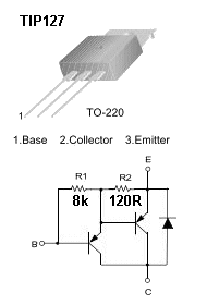
The circuit will not work because the author failed to realise the Darlington TIP127
transistor has inbuilt resistors. To pull the base down by a voltage equal to
0.7v plus 0.7v, resistor R3 must be less than 60k. At 60k, the transistor is
just at the point of turning on.
Page 1
Page 2
Page 3
Page 4
Page 5
Page 6
Page 7
Page 8
THE MISTAKES!
Page 15
Page 10
Page 11
Page 12
Page 13
Page 14
Page 16
Page 17
![]()
I have seen so many faulty designs in an Indian magazine: Electronics For
You, from writers who have a list of qualifications after their name, that
it makes their degree in electronics questionable.
I know no-one likes to be criticized but when you are teaching how to design a
circuit, it is important the circuit not only works, but is designed
correctly.
It is not good enough for a circuit to work, it must be designed correctly so it takes the least current and requires the least number of components.
Every component has a "technically correct" value for each position in a circuit
and that's what we teach. When the component-values are outside this range, it
is obvious the engineer is lacking the skills in circuit-design. However if the
circuit specifically requires a certain value, mention it on the diagram.
That's what a circuit is for. It MUST show all the values of all the components.
It's a stupid idea to have a List Of Materials. Only an IDIOT would draw a
circuit with R1, R2 etc and provide a list of values. He obviously have
absolutely no electronics ability AT ALL. I can work out what a circuit is
doing by looking at the component values. That's why this website is so
important. It is teaching ELECTRONICS UNDERSTANDING.
The traffic to our site is increasing all the time and it has just reached 7,000
visitors per day.
This is spread over hundreds of articles, but the eBooks
are getting most of the readers while those that are really interested in
electronics are reading through the 14 pages of Spot the Mistake.
This type of teaching has never been done before, and I wish it was available
when I stated in electronics.
You learn more from other's mistakes than a whole book of successful circuits.
![]()
DICE
Electronics For You magazine is filled with mistakes and these will keep
us busy for years to come.
Here is a DICE project with a number of mistakes: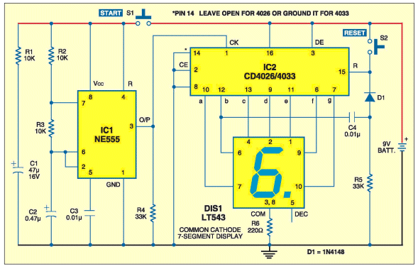
A single resistor on the common line of the display will make the segments fade
when a lot of segments are illuminated. To keep the segments equal-brightness, a
resistor is needed on each drive-line.
The diode on the reset line serves no purpose. In fact it is creating a high
impedance on the line and can cause a reset at any time. It should be removed.
![]()
It has lots of design-faults.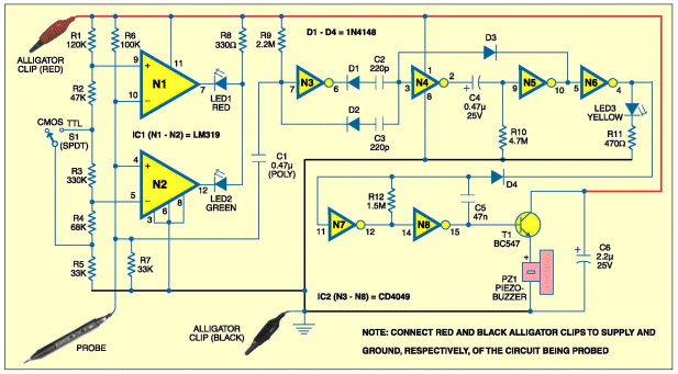
The input is sitting HIGH so the output will be LOW.
Only a HIGH-to-LOW transition on the input will change the state of the gate.
This means the output will go HIGH.
It does not matter what voltage is on the anode of Diode D1, any rise in voltage
on the cathode is not passed through the diode. That's not how a diode works.
The diode is around the wrong way.
Now let's look at Diode D3. The input of N5 is LOW so the output is HIGH. No
current can flow through the diode to the input of N4 and thus this inverter
sits with an unknown voltage on the input.
Now let's look at the yellow LED. To turn on the pulse LED (yellow), the output
of N6 must go HIGH. The input to N6 must go LOW and this means the input to N5
must go HIGH.
For the time-delay circuit (made up of C4 and R10) to work, Pin2 must be HIGH
and C4 must be charged. Pin 2 goes LOW very briefly and the fully charged
capacitor gets instantly discharged via pin 2 and the input protection diode on
the input of N5. Pin 2 then goes HIGH and brings C4 HIGH and puts a HIGH on pin
9. This illuminates the yellow LED.
The capacitor gradually charges via the 4M7 resistor and this creates the delay.
But for this to happen, pin 3 of N4 must be LOW and if D1 is turned around the
other way, pin 3 will be taken HIGH when a pulse is detected. D2 and C3
are not needed. A 4M7 is needed between pin3 and 0v rail and D3 is not needed.
This circuit is certainly a mess.
![]()
This circuit has a number of technical mistakes.
I have received a reply from Electronics For You, and the replies are in 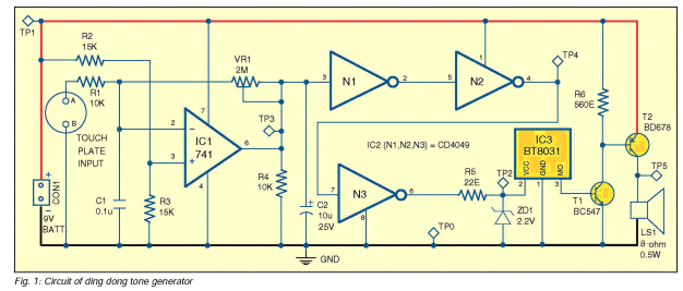
There are many ways to design the circuit to
get the same output. This circuit shows the use of inverter and 741 op-amp
- but a circuit should be as simple as possible
- not as complex as possible.
The need for the 10k resistor (R1) is unknown. It serves NO purpose.
The need for the 10k resistor (R4) is unknown as the op-amp pulls low.
You will not know unless you wire and check
yourself. What sort of answer is this?
Gates N2 and N3 are not needed as they simply produce the same result as the
output of N1.
Not in this case. N2 and N3 gates are needed,
there are reasons behind it.
What sort of answer is this?
The 22E (22R) resistor R5 is far too low. The CD4049 can source 10mA and to
deliver this current to the 2v2 zener requires a 560R resistor.
You have no idea why we use these values. Your
doubt is based on theoretical observations.
The reason why the
The output of the BT8031 requires a buffer resistor on the output of about 1k.
The IC should not be connected directly to the base of a transistor. See the
data sheet.
The output current of BT8031 is less than
2mA.
You don't need a buffer resistor at its output
pin in this design. We have the datasheet of BT8031.
The data sheet clearly shows a 5k to 10k
resistor on the output.
The BT8031 is actually BT8031-02 for the Ding Dong version.
OK you say so. We have
not seen or used BT8031-02
The BD678 is actually a PNP Darlington transistor and should be drawn as a
Darlington.
Normally we used
transistors symbols either npn or pnp irrespective of Darlington or not. This
SAVES time and space. But your point is noted.
The BC547 transistor is not needed as a PNP BD679 transistor could be used as
the buffer transistor.
The BT8031-02 can be supplied with 3v and it may be necessary to deliver 3v to
drive a Darlington transistor.
There is no current limiting resistor on the collector of the BC547. Without
this resistor a very large current will flow through the junctions of the two
transistors when driving the speaker and this is WASTED CURRENT.
The value of R6 is technically too low. It should be 10k.
Your doubt is based on
theoretical observation. The design is working fine and no changes are required.
The circuit may be "working fine" but it has so many technical
faults that it is obvious the designer of the circuit has no technical ability
AT ALL. This would be ok if he just produced the circuit for himself, but it is
being presented in an electronics magazine for thousands of readers to study and
observe and it should be technically correct. ![]()
This is one of the worst-designed Delay circuits: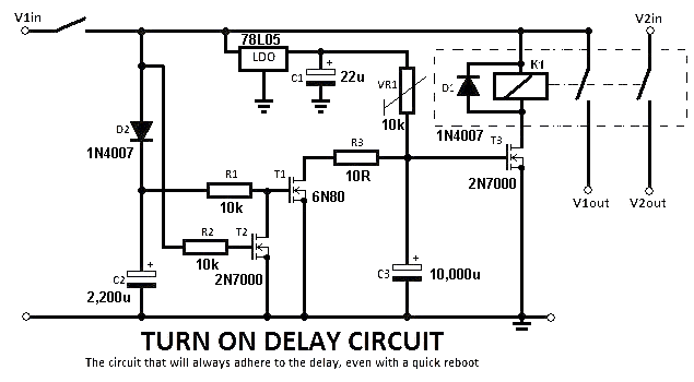
The delay is made up of a 10k multi-turn pot and 10,000u electrolytic. Normally a
delay is made up of a high resistance and low value capacitor. The mid-point of
these two components is then taken to a high impedance detecting circuit. In
this case it is the gate of a FET. The 10k should be increase to 100k or higher
and then the capacitor can be reduced to 100u to 220u.
A muli-turn pot is the worst choice of pot as you don't know where the wiper is
positioned. 10-turn pots are NOT designed to be constantly adjusted.
The 1N4007 diodes can be changed to 1N4004 to show that 1,000v diodes are not
needed.
The value of R1 and R2 should be increased to 47k to show the surrounding
circuit is high impedance.
The 78L05 is not a LDO (Low Drop Out) Regulator.
The designer of the circuit says "resistors of high values are less durable"
What does this mean? If he means they are less reliable, it is not true. A
100k or 470k resistor is just as reliable as 10k.
The designer suggests a 3v3 regulator. The 2N7000 requires up to 3v to turn ON
when 75mA is needed. If the relay needs 100mA or more, the gate may require
slightly more than 3v and the circuit will not work.
The circuit is over-designed and uses expensive components.
![]()
Here is another over-designed circuit: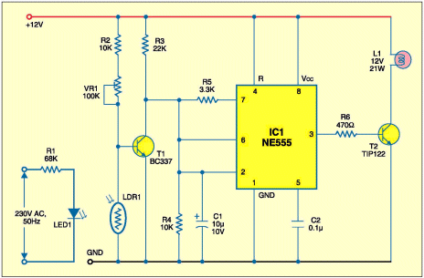
![]()
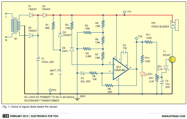
2. D1, D2 and D4 should be identified as 1N4002 to indicate the
reverse-voltage only needs to be 100v. A 1N4007 is a 1,000v diode.
3. The output of a 9v - 0v -9v transformer will be a lot higher than 9v
on NO LOAD due to the poor regulation of these types of transformer. The output
voltage is designed to fall to 9v on full load. This means supply rail will be a
lot higher than 12v and the 9v battery will be overcharged via the 68 ohm
resistor.
4. R3 R4 and R6 can be converted to a single resistor.
5. You cannot drive a diode through a 10M resistor and expect to get a result.
Any voltage-change will be partially or wholly absorbed by the 10M resistor.
6. What does C2 and R8 do? There is nothing at the join of these two components
and they perform no function when connected in series. This type of arrangement
is only used when the circuit is oscillating at a fairly high frequency. When it
oscillates, the 10k and 22k resistors produce a voltage-divider that is detected
by the inverted input of the op-amp. This feature does not apply when the change
is very slow.
7. The value of 10p for C3 will have no effect on the circuit.
8. The maximum output current for a CA3140 is 40mA for a 15v supply. The
supply will possibly be about 15v due to the point mentioned above and the
output will be about 10v due to the arrangement of the 10M resistors and the
fact that the output is connected directly to the inverting input. It is unknown
what current will be delivered to the LED but the 100R on the LED will make the
output very low impedance and the maximum output voltage is unknown.
9. The op-amp will have UNITY GAIN in this arrangement and that is one of the
big mistakes of the circuit.
10. The value of R11 is too low. When the pot is turned fully clockwise, up to 30mA
may flow through the zener and base-emitter of the transistor.
It's just a bad design. Many of the values are far from "design values." Design
Values are those you would find in a properly designed circuit.
That's 10 mistakes in a single circuit.
One reader: "amspire" produced a list of answers that were entirely incorrect. I
will go though his list:
Component values should be shown for a reason. A beginner to electronics may
wonder why a 1,000v diode is needed. That's why the circuit should show 1N4002.
You do need a
compensation cap on that opamp otherwise it is not stable at unity gain - it is
100% guaranteed to oscillate without the 10p cap.
A 10p capacitor will have NO EFFECT on reducing the instability. There is no
mention of the need for a compensation capacitor in the data sheet.
The 10Meg resistor does not
swamp out the diode. At low temperatures, it is the diode that swamps out the
10M resistor.
This is entirely UNTRUE. The 10M resistor in series with the diode will reduce
the voltage-change (from the diode) entering the op-amp by a ratio equal to the
10M to the input-resistance of the op-amp. The input impedance of the op-amp is
less than 5M and thus less than 35% of the voltage-change will be detected.
C2 and R8 increase the sensitivity to a fast rise in temperature.
The voltage-increase from the diode is very slow in terms of op-amp speed and
the capacitor will have no effect.
The maximum that can flow into the transistor base is probably 15mA with the pot
at full (and it will not be at full after adjusting) and 15mA will not damage
the transistor or zener so that is absolutely OK.
The circuit is so badly designed that you cannot find a starting-point to
discuss this section.
However the zener diode is not needed as the voltage-drop across it is NOT 3v1.
It will start to leak at a much lower voltage and the transistor will turn on.
The zener serves NO purpose.
There are no "design values" for a transistor that you
should adhere to - you can do absolutely anything you like with a transistor as
long as you do not exceed limits and blow it up. Even Maximum ratings can be
exceeded if you know what you are doing - eg using a transistor in avalanche
mode for a fast pulse generator. I can go through the whole list, but you
have not identified a single fault.
It is lucky we have websites like Talking Electronics to show you how to design
a circuit. Of course there are "design values" like 470R feeding a LED and 4k7
to 10k feeding the base of a transistor.
This circuit was sent to Electronics For You via their request in the
February issue:
Mr Mitchell is a Critic of all circuits published in EFY and he is
tarnishing the Indian publications and authors. So I am not interested to reply
to his queries.
The reply from the "Technical Editor" was:
Where are these technical personnel????
Why didn't he send my corrections to one of these "technical people"?
Obviously the magazine does not have any technical personnel as it has been
publishing circuits with hideous mistakes for over 10 years. Nearly every one of
their circuits has technical faults and they don't even want anyone to correct
them.
I call this sabotage. They are sabotaging electronics enthusiasts by feeding
them with faulty designs and making their chances of successful employment
almost zero.
It's people like this and magazines like Electronics For You that
should not be in the publishing business. They are just ruining the name of
electronics.
![]()
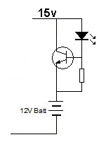
When the voltage on the base of T2 is 0.55v, the transistor is not turned on.
When it is 0.7v, the transistor is turned on. The 470u C2 is only used for this
small voltage range.
By placing a resistor between C2 and T2, (on the base) the voltage-range will be
increased and its effectiveness will be increased.![]()
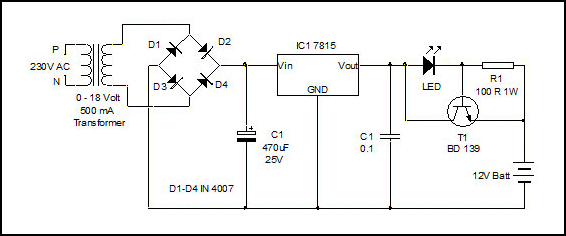
![]() Here's another D.Mohankumar circuit:
Here's another D.Mohankumar circuit:
![]()
![]()
What is pulling the base LOW when the power fails? Another untested circuit.
![]()
![]()
The operation of this circuit is very clever and quite complex. See the full
explanation of how the circuit works in "101-200
Transistor Circuits".
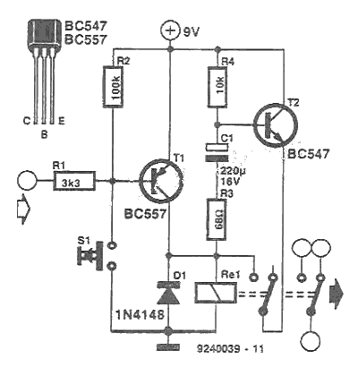
Toggle A Relay![]()
The connection of the first three transistors looks unusual, so the circuit was
drawn in an understandable way. 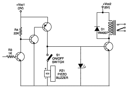
When the first transistor is NOT turned on, the second transistor is turned on
via the 22k resistor and this pulls the base of the third transistor towards the
0v rail. The emitter will have about 0.9v on it and the current through the two
transistors will be very high.
This is an extremely BAD design.
The voltage on the collector will be about 0.7v. The transistor driving the
relay will turn on but the LED on the base will not illuminate and the Piezo
Buzzer will not produce a sound.
When the first transistor is turned ON, the second transistor is turned OFF and
the third transistor is turned OFF.
What a terrible design.
Electronics For You informed me they do not have a technical that
understands electronics technology and simply publish the circuit because "it
works."
Now you can see how damaging this simplistic approach is. 40,000 young
electronics enthusiasts are a getting the wrong idea on circuit design because
the magazine does not know how to test a circuit. ![]()
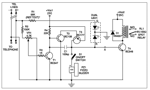
It's an FM Bug that connects across the phone line. All Talking Electronics
Phone Bugs connect to one of the lines by cutting the wire and inserting the
circuit. A bridge on the circuit automatically adjusts to either polarity and
you don't have to worry about the high voltages of the phone line.
The following circuit is a disaster. The output transistor is a 20v device
and it will zener (actually break-down) when connected to the line and that's
why the "laboratory" at
Electronics For You had to add the 22k. Instead of working out why the
circuit engaged the phone when connected to the line, they added the resistor.
But the major faults are:
The 47k resistor is not connected to the top rail and the oscillator transistor
i s not turned ON.
The coil in the collector does not have a capacitor across it to make a TANK
CIRCUIT and the circuit will not work.
C1 should be connected to the base of the transistor.
C2 is not needed.
That's 5 faults in a single circuit.
Another terrible design. 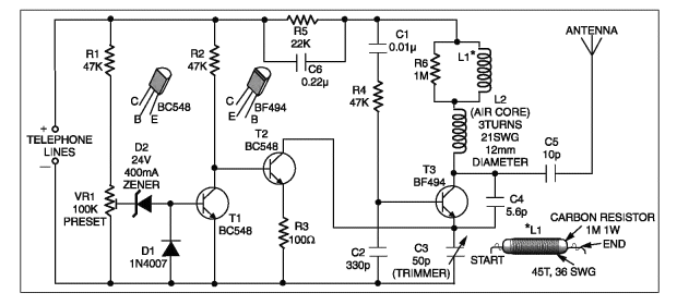
![]()
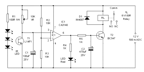
Here's an over-designed circuit, with mistakes. If the 10k is turned clockwise,
pin 7 will be damaged. 
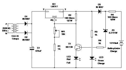
![]()
This circuit delivers 7.5v and the battery will gradually DRY OUT. The circuit
needs to be redesigned with a current-limiting resistor or a power diode on the
emitter of T1 to reduce the output of the regulator to 6.8v. 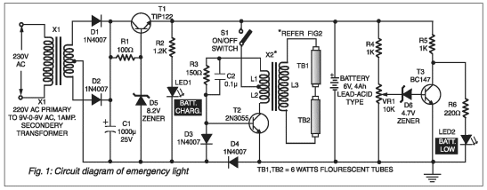
![]()
This circuit detects heat via the thermistor. As it gets to
100�C, its resistance decreases to about 1k.
The diode, R2 and electrolytic are not needed. By adjusting the value of R8, the
voltage on the base of T1 can be sent so the circuit turns on at an elevated
temperature.
As the voltage on the base of T1 increases, the transistor turns on and the
emitter rises. This means the voltage on the base must rise higher to turn the
transistor on more. This is not a problem in this circuit but resistor R3 (470R)
should be in the collector of T1 so that a rise in base voltage will be passed
to the output.
The worst feature of the circuit is the current-drain. The circuit takes 10mA
and most fire alarms take only a few microamps so the battery lasts for a year
or more.
By connecting pin4 and 8 of the 555 to the collector of T2, the chip will not be
powered during the waiting period and the circuit will take much less current. 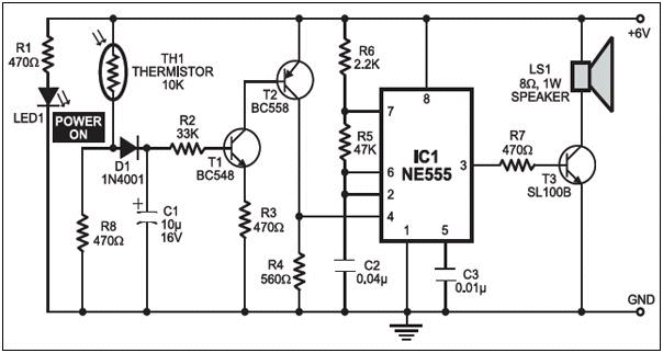
![]()
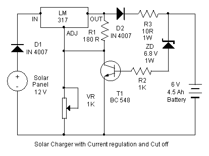
A zener diode is not designed to be used as shown above. A zener diode is very
"leaky" and any voltage on the cathode is transferred to the other lead and it
will appear on the base of the transistor.
That's what is happening in this circuit and the output only has to rise to 0.9v
and the transistor is already turned on and taking the adj terminal of
the regulator to 0v rail.
This circuit does not work. Another untested circuit by D.Mohankumar.
Why use a 12v panel to charge a 6v battery? This makes the circuit less than 50%
efficient.
Why have any electronics AT ALL? A 4.5aHr battery can be constantly supplied
with 300mA and it will not be overcharged. Use a 6v 300mA - 500mA solar panel
with a single diode to prevent current flowing back into the panel when it is
not illuminated. That's all the circuitry you need as the panel will be
supplying energy for no more than 8 hours per day and the battery will not get
overcharged.
You have to think "outside the square" and ask: "Is a complex circuit
necessary?"![]()
The 10k base resistor to the first transistor is far too low. It should be at
least 100k.
A low-value resistor will reduce the incoming waveform from the microphone by
about 50%.
The electret microphone will produce a waveform of about 2mV to 20mV. The first
transistor will have a gain of about 100. The result will be a maximum of
1,000mV
The second transistor is an emitter-follower and will not increase the amplitude
of the waveform.
The third transistor has a fixed gain of 10 due to the ratio of the 10k
collector resistor to the 1k emitter resistor.
The circuit will produce sufficient waveform (about 1,000mV x 10) to turn
on the fourth transistor but the 10u feeding the diodes is around the wrong way
and the 4u7 will have a greater effect if it is away from the base by adding a
4k7 resistor. ![]()
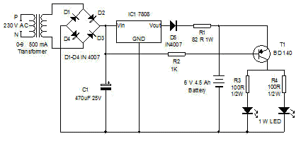
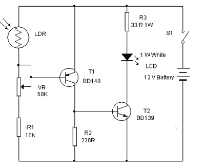
EMERGENCY LIGHT
If the pot is turned fully clockwise, the BD140 will take more current and this
will flow through the base-emitter junction of the BD139. This current will be
more than required by the BD139 and it will be damaged.
The current taken by the 1watt LED will be 12v - 4v = 8v / 33 = 240mA. The
wattage of the 33R should be 8 x .24 = 2 watts.
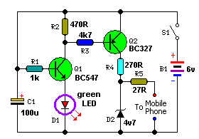
![]()
Transistors are not added to a circuit to make it more complex. These
transistors are NOT NEEDED.
![]()
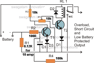
1. The value for R1 is 0.12 ohms for 10 amp load due to the fact that diode D3
has been placed on the emitter of transistor T1. This diode is not needed.
Removing the diode allows R1 to be 0.06 ohms and 6 watts instead of 12 watts.
A huge difference.
2. D1 is not needed. It serves NO purpose.
3. The value of R4 is far too high. It will NEVER keep T1 in conduction. R2
needs to be increased to 10k and the circuit will work.
Obviously the circuit has never been tested. Two unnecessary parts and two
incorrect-value resistors.
![]()
![]()
I have only identified the 7805 and 4017 as this is where the fault lies: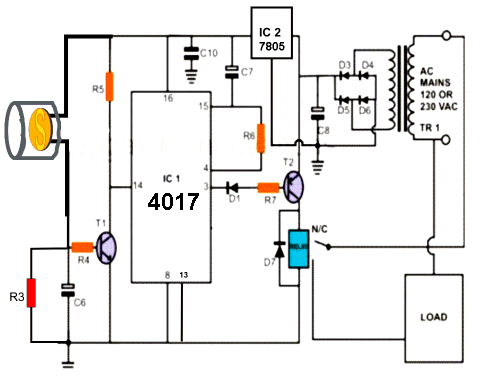
The output of the 4017 cannot rise higher than 4.5v. To turn off the PNP
transistor (T2) the base voltage must rise to about 11.5v
In this circuit the transistor will NEVER TURN OFF.
That's why you use an NPN transistor on the output in this type of circuit. You
can then use different-voltage supplies. ![]()
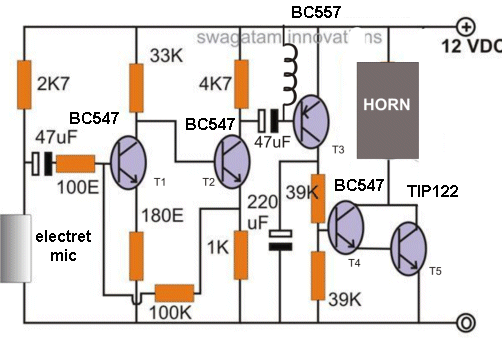
The 100 ohm resistor on the base is not needed. It serves no purpose.
The "coil" on the base of T3 is an unknown component and should be removed.
The two 39k resistors on the input to the "Darlington" arrangement should be
100k so the 220u can be reduced to 100u. ![]()
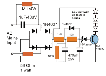
Suppose we remove the LEDs and see what happens.
The result is 330v on the output of the bridge, 172v on the first electro
and 15v on the second electro. The transistor now turns on and the 25 white LEDs
produce a voltage-drop of 75v. The voltage on the first electro drops to 45v,
but it will
blow up. The 100k must be reduced to 10k.
Now we come to the next problem.
The 1u capacitor will deliver 70mA and in this type of circuit the 70mA current
is being delivered to the load and it must be able to accept (dissipate) the
wattage. The wattage will depend on the voltage across the load and in this case
we have two paths. The 10k plus 10k plus 15v zener path takes 3mA because the
supply is 75v.
The remaining 63mA will flow though the white LEDs and BLOW THEM UP it they are
ordinary LEDs. They have to be high-wattage LEDs and although 1watt LEDs require
300mA for bright illumination, 63mA will produce a very good output.
As you can see, the physics behind this simple circuit is much more complex than
you think. ![]()
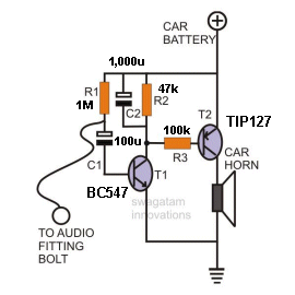
Now we come to the next problem.
A car horn requires about 4 amp to produce an output. But the coil inside the
horn is only being activated for about half the time and this means the starting
current to activate the electromagnet is 8 amps. This point has never been
mentioned before and is one of the hidden problems with driving a horn.
To fully drive the transistor (fully saturate it), the base current must be
increased and the base resistor will have to be reduced to 33k. ![]()
Page 9
Page 10
Page 11
Page 12
Page 13
Page 14
Page 16
Page 17
