SPOT
Page 1
Page 2
Page 3
Page 4
Page 5
Page 6
Page 7
Page 8
Page 9
None of the "panel of experts" explained how the circuit works. None of them
noted the absence of the current limiting resistor for the LED or the reason why
the base resistor is so high.
Diode D1 only needs to be 1N4004.
DANGEROUS POWER SUPPLY
THE MISTAKES!
Page 17
Page 10
Page 11
Page 12
Page 13
Page 14
Page 15
Page 16
Page 18![]()
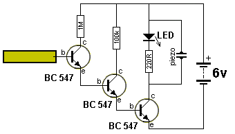
It is surprising how some electronics hobbyists and those working in electronics, can
exist in this field with a faulty or limited knowledge of electronics.
I take the example of an electronics forum where a reader asked a simple
question about a LED and dropper resistor. He provided a circuit and wanted to
know why the base resistor was so high.
Here is the circuit: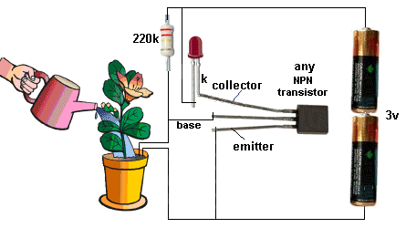
The transistor is turned on very lightly. It will amplify the current though the
220k resistor by a factor of say 200 (the gain of the transistor) and this will
be equal to putting a 1k resistor in the collector circuit. The current will be
only 1mA to 2 mA.
![]()
Here in another of professor D. Mohankumar's circuits:
We are not going into the operation of the circuit because it DOES NOT WORK
However here are some of the faults: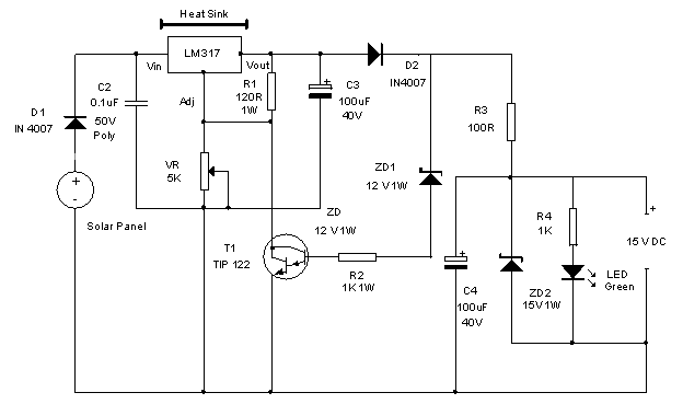
T1 does not need to be a power Darlington transistor. It can be BC547.
The output voltage will never reach 15v. The Darlington will turn on when the
output voltage is 11.5v + 1.2v = 12.7v. Yes a 12v zener starts to "leak"
at 11.5v. No-one has ever told you that a zener starts to turn ON at a lower
voltage. That's why they cannot be used in a circuit as shown above. You
need a resistor between the anode and 0v to remove the leakage at 11.5v and wait
for the major breakdown at 12v.
The output will NEVER rise above 12.7v
Suppose the circuit is supplying 100mA to the battery. The voltage drop across
the 100R resistor will be = 0.1 x 100 = 10v !!
Can you see how absurd this circuit is?
It has never been tried or tested.
![]()
This circuit is the most dangerous Power Supply you can get:
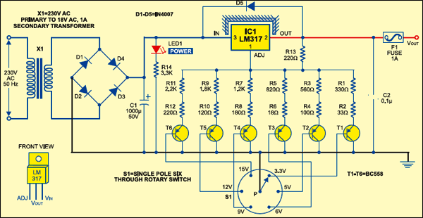
When the switch is changed from one voltage to another, the output instantly
increases to more than 18v and will blow up many circuits.
The BC557 transistors are not needed as the resistors can be connected to the 0v
rail via the switch.
However the 220R resistor (R13) is the resistor that should be changed and the
circuit needs to be totally redesigned.
This circuit comes from Electronics For You. This Indian magazine is
fooling the readers by saying they have electronic engineers and have tested the
circuit.
I have asked for the names of the "electronic engineers." They have NONE.
It's rubbish like this circuit that makes Electronics For You a total
failure as a magazine. They don't have anyone to check the accuracy of a circuit
and "just because it works" they publish it.
Both
Professor Vidyasagar and
Professor D.Mohankumar supply projects to Electronics For You and
we have shown how incompetent they are.
Professor Vidyasagar has now removed his website completely from the
internet, after I sent him over a dozen emails with his faulty reasoning and
circuits that don't work. At least he has woken up to the fact that you can't
fool "ALL THE PEOPLE ALL THE TIME."
D.Mohankumar's website
![]()
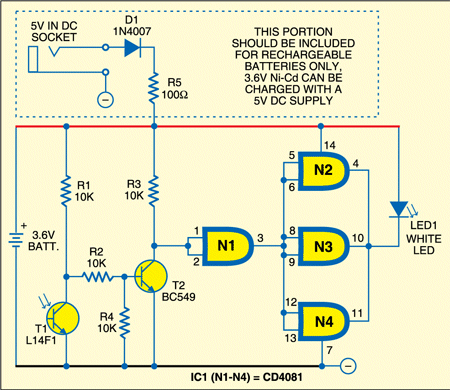
Here's another impractical circuit from
Electronics For You:
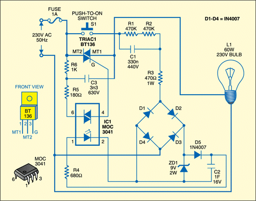
This circuit allows you enough time to reach your bed and lie down before the
bedroom lamp switches off automatically.
Mains power supply is reduced by the capacitive dropper arrangement. A 1F
capacitor (C2) handles the timing part. When switch S1 is pushed to �on�
position for a few minutes, bulk capacitor C2 charges and the stored energy
drives the internal LED of IC MOC3041 through resistor R4.
Who is going to push the switch for "a few minutes"
1F @ 5.5v is $3.00 to $19.00 depending on the supplier. eBay is the cheapest -
it always is.
Where can you get a 1,000,000u (1F) capacitor @16v ??
The circuit only charges the supercap to 8.5v and thus half the possible energy
is wasted. The only 1F @16v supercap on the web is very large and costs about
$100. What an impractical circuit. Doesn't
Electronics For You test anything?
1F capacitor can store one coulomb of energy @ 1v. Thus 1F @ 5.5v supercap
can store 5.5 coulombs of energy.
But it can only be discharged from 5.5v to 2v (as this is the
characteristic voltage across a LED). Thus the cap can supply about
3 coulombs.
1 coulomb is 1 amp x 1 second
If we allow 20mA for the LED, it will be illuminated for (3 x 1,000) / 20 = 150
seconds.
It will take as long to charge the supercap as discharge it. The charging
current is about 20mA and the 9v zener does not come into operation until the
cap sees 8.4v.
![]()
Here's another circuit that doesn't work, from
Electronics For You:
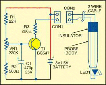
The transistor controls the brightness of the super-bright white LED in the tip
of a pen.
The article states:
The ultra-bright LED requires up to 20 mA for full brightness. So there is no
need for a separate on/off switch. Disconnecting CON1 from CON2 is enough when
not in use.
Two major faults with the circuit:
1. Current will flow through the 22k and 220k pot and 560R resistors when CON1
is removed and the battery will go flat.
2. The maximum current through the 220R resistor will be:
The voltage across the white LED is about 3.2v. The voltage across the
collector-emitter of the transistor is 0.2v so the voltage across the 220R will
be 4.5v - 3.2v - 0.2v = 1.1v
The current through the 220R will be 1.1 / 220 = 5mA !!!!
Another untested circuit from
Electronics For You.
![]()
Here's another stupid circuit from Electronics For You:
The LED illuminates when T1 is not illuminated.
Two major faults:
1. Current will flow through the 10k and T1 when illuminated (about 3mA) and
this will flatten the battery.
2. What is the purpose of the IC ???? It serves NO purpose. Simply connect
the LED to the collector of the transistor via a low value resistor.
Another pointless circuit from
Electronics For You.
![]()
Here's another fault from Electronics For You (April 2013 issue):
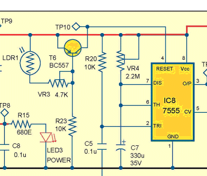
The reset-line of a CMOS 7555 IC is connected to the gate of a FET and it
requires almost no current to provide the reset feature.
The reset line is active LOW and this means any voltage above about 1v DOES NOT
reset the chip.
When the voltage falls below 1v, the chip is reset.
Even though NO CURRENT is required by the line, you MUST pull the line low via a
resistor so that the gate sees a LOW VOLTAGE.
In the circuit above, the transistor pulls the gate HIGH to keep the chip
activated, but when the LDR sees illumination, the voltage between the base and
emitter is less than 0.6v and the transistor "turns off."
This makes the collector lead a HIGH IMPEDANCE LEAD and it is just like removing
the transistor from the circuit. This leaves the reset line "floating" and there
is nothing pulling the line LOW. It requires 100k to 1M from pin 4 to 0v.
This is a major fault in the design of the circuit due to the author not knowing
the internal features of the chip.
Electronics For You also failed to pick this up because they have no
technical staff to diagnose and check a circuit.
This leaves the experimenter in the invidious position (likely to arouse or
incur resentment or anger in others) of finding the circuit does not reset and
thinking he has made a mistake.
![]()
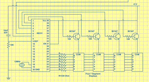
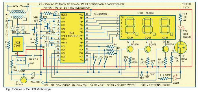
Here's another fault from Electronics For You (April 2013 issue):
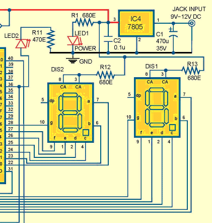
7-segment displays should have a current limiting resistor on each line (a,b,c,d,e,f,g)
so that each number (0,1,2,3,4,5,6,7,8,9) will illuminate with the same
brightness.
In the circuit above, the common line has a 680R resistor and when a single
segment is illuminated, 4mA will flow through the segment. When two segments are
illuminated, each segment will get 2mA. When all 7 segments are illuminated each
will get 0.5mA. The display will get duller and duller.
Obviously the circuit has never been tested.
Each line should have a 220R resistor and the common line is connected directly
to 5v.
This project has been designed by Sani Theo, the Technical Editor for the
magazine.
You can now see why the magazine has so many faults.
![]()
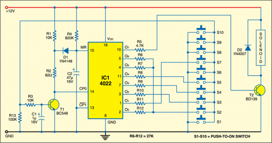
Here's another untried, untested circuit from Electronics For You (April 2013 issue):
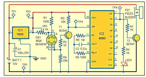
The Gas Sensor is supposed to be connected DIRECTLY to 5v, not via 100 ohm
resistor.
The Gas Sensor has a heater that draws 150mA @ 5v (750mW) and if a 100 ohm
resistor is added, the heater will take 37mA. (the Gas sensor heater has a resistance
of 33 ohms).
This circuit has never been tested and may or may-not work with 37mA heater
current, but it will certainly take longer to make a reading because the idea of
the heater is to burn the air-gas mixture and take a resistance reading from a
ceramic substrate.
This circuit has been supplied by Professor Mohan Kumar and we have already
identified him as being completely inept at designing electronics circuits.
![]()
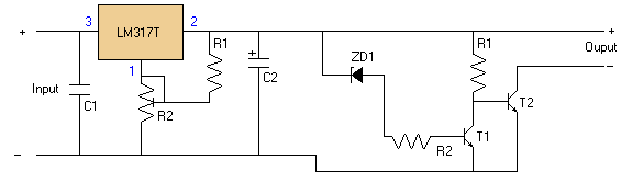
Here's another untried, untested circuit from Electronics For You (April 2013 issue):
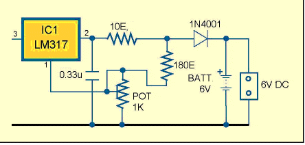
We start the discussion with just the LM317 3-terminal regulator.
It is designed to produce a voltage of 1.25v above the voltage on the adjust pin
(pin 1) and it monitors this voltage accurately.
This means the output voltage will be 1.25v when the adj pin is connected to 0v.
If we add a 180R resistor and 1k pot, we can "jack-up" the output voltage until
the output is about 2v less than the input. (This 2v is needed by the circuit
inside the IC.) If this voltage is delivered to a load, the chip will deliver up
to about 1.5amp.
Now we add the 10 ohm resistor.
This resistor is called the CURRENT LIMITING resistor and normally it is added
as shown but the 180R and 1k pot is removed and the adj pin is connected between
the 10R and diode.
For a 10R resistor, the maximum current is 125mA
When this is done, the output voltage will rise to any voltage (that is about 2v
less than the input voltage) and as the voltage rises, the current through the
load will increase and also through the 10R resistor, (because they are in
series).
As the current through the 10R increases, the voltage across it increases and
when it reaches 1.25v, the circuit inside the IC detects this and the
output voltage stops increasing.
When we add the 180R and 1k pot, we have an unusual situation.
We can increase (jack-up) the voltage on the output to about 8v but when we add
a load, the 180R alters the current limiting to 35mA.
If the circuit requires 35mA charging current, a 33R resistor can be used and
the 180R and 1k pot can be removed.
You cannot add both features at the same time. If you try to set the output
voltage, it will decrease rapidly as current is drawn.
Another untried, untested circuit from
Electronics For You.
![]()
Here's another faulty circuit from Electronics For You website:
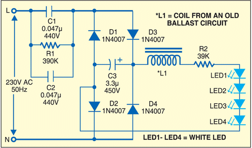
You have to work out the total impedance of the circuit.
This is 31k for the .047u + 0.47u (in parallel) and 39k for R2.
This means the current through the circuit will be 3.4mA
How bright will the LEDs be with 3.4mA !!!!
![]()
Here's another faulty circuit from Electronics For You website:
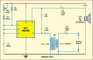
The output of a 555 can only deliver 200mA to a load and this means the
impedance (resistance) of the load must be 60 ohms or more for 12v supply.
However we have another factor that must be taken into account. The chip can
only dissipate 600mW.
This means the output must be derated to 50mA when the supply is 12v.
Neither of these factors have been taken into account with the circuit above.
If we take a frequency of 500Hz, the capacitive reactance of 470u is LESS THAN
ONE OHM !
This makes the output less than 10 ohms !
Another untried, untested circuit from
Electronics For You.
![]()
Here's another terrible circuit from
Electronics For You website.
This circuit has been designed by Sani Theo - one of the Technical people at
Electronics For You. He has absolutely no idea how to design a circuit:
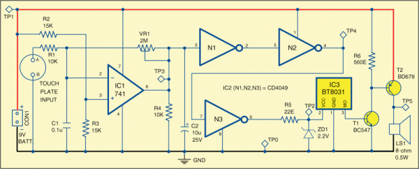
This circuit has lots of mistakes. Apart from the fact that it does not work, here are the technical faults:
1. The output of the 741 sits at half-rail-voltage. This is a very bad voltage
to deliver to a digital gate as it causes the gate to oscillator at high
frequency. The output of the 741 should go to a very low voltage to provide a
genuine LOW to the Inverter gate.
2. The output of pin 6 is low impedance. There is no point in placing a 10k on
pin 6 to 0v rail.
3. C2 serves no function. Pin 6 is low impedance and the electrolytic has no
effect.
4. Gates N2 and N3 have no effect on the circuit and can be removed.
5. R5 22R is far too low to protect the output of the Inverter
gate.
6. IC3 needs a 1k on the output as shown in the specification sheet.
7. R6 is far too low for the position shown. It should be 4k7 to 10k.
8. T2 is a Darlington Transistor and should be shown as a Darlington.
9. There is no current limiting resistor between T1 and T2 and more than 100mA
will flow though the base of T2 as wasted current.
10. There is no delay to allow the music IC to produce the Ding Dong sound.
That's 10 poor designs in a simple circuit from someone who touts himself as a
Technical Editor. What a disaster.
![]()
Here's faulty circuit from Electronics For You from the year 2000:
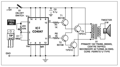
The transistors are directly connected to the power rail via collector-emitter
and base-emitter junctions and when the transistors are turned ON, these
junctions have a very low voltage across them. This means a very high current
will flow.
The actual current will depend on the base current from a previous stage and the
CD4047 can deliver 10mA. If the transistor has a gain of 100, this means a
wasted current of 1AMP will flow through the transistors, and especially the
base-emitter junction, which is not designed to pass this high current.
![]()
Here's a faulty animation from:
http://electronicsgurukulam.blogspot.com.au/2012/07/cathode-ray-tube-animation.html
The animation is entirely wrong.
The beam is deflected in the neck and then it travels in a STRAIGHT LINE to the
screen.
![]()
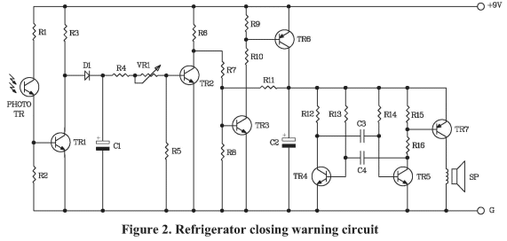
Here is over-designed circuit by D. Mohankumar:
It detects if a cable is carrying the "mains."
All you need is 3 transistors and you can add a piezo diaphragm to hear the
"mains."
MAINS HUM DETECTOR
![]()
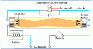
http://electronicsgurukulam.blogspot.com.au/2012/11/tubelight-starter-working.html
Argon gas of this length would normally take thousands of volts to "strike."
The tube is connected as shown in the diagram and when power is applied, the starter starts to glow.
Current will not pass through the tube because the gas inside it is not ionized and it behaves as a open circuit.
The starter contains a tube with neon gas and this gas needs about 70v to 90v for it to glow.
Also inside the starter is a bimetallic switch that is open. The glowing gas heats up the bimetal strip and it closes.
This allows current to flow through the ballast and the filaments at the ends of the fluorescent tube.
The filaments heat up the gas in the tube (at the ends) and the mercury vapour and the electrons are excited.
The gas in the starter ceases to glow (because the bimetal strip has closed) and the bimetal strip cools down and opens.
This allows the current in the ballast to collapse and it produces a higher voltage.
This voltage (together with the mains voltage) is sufficient to "strike" the tube and immediately the voltage across the tube drops to about 90v.
The ballast now takes up the difference between the supply voltage and the tube voltage.
If the tube were placed directly across the supply, it would take a very high current and blow up.
The voltage across the starter is now not enough to re-strike the neon gas and it remains "off."
![]()
Electronics For You and
T. K. Hareendran will never learn.
Here is another JUNK circuit from the April 2103 issue of EFY.
I have emailed both on many occasions to send me any circuit before publication.
They have failed to do this and prefer to show how stupid they are.
1. There is no current-limiting resistor between the two transistors. If
the first transistor is turned on via 2mA into the base, the collector will pass
200mA or more.
2. Each string of LEDs has a characteristic voltage drop of 3.2v x 2 = 6.4v.
The voltage across the 1k resistor will be less than 3v and 3mA will flow
through each LED.
3. Why use a power transistor BD140 to pass 30mA !!
What a useless, badly designed circuit. The current through the transistors is
more than through the LEDs.
Another useless, untried, JUNK circuit to mess-up Indian experimenters.
T. K. Hareendran has emailed me to say his prototype used 150R resistors and
for some reason they were changed to the absurd value of 1k. That's
Electronics For You !!
T. K. Hareendran has added the fact that the circuit takes 130mA through the
transistors as wasted current.
The prototype was re-tested with a 1K5 resistor between base of T2 and collector
of T1, and the efficiency improved considerably.
That's why you have to take a reading of the current taken by the circuit in all
states and conditions, just in case something is faulty.
![]()
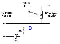
Here's a terrible explanation of how a Diode Pump works from Professor D. Mohankumar.
email:
mohanwordpress@gmail.com
His circuit had the 10u around the wrong way. But his explanation is not only
incorrect, but almost impossible to understand.
When the waveform from the 10u tries to go below 0 volt, the first diode takes the current from the negative rail. Therefore voltage never goes below 0 volt at the junction of the 10u and the diodes. When the waveform from the 10u rises, the rise is from minimum (0 volts) as imposed by the first diode. Since the waveform is not changing, the total voltage between the upper and lower peak of wave is then pumped into the top diode and then into the 22u.
No wonder Indian students don't understand electronics - I cannot understand what he is trying to say.
Here is a clear description of how the circuit works:
Circuit C is a DIODE PUMP (VOLTAGE DOUBLER)
from an AC source (such as the "Mains").
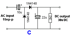
The circuit takes a number of cycles to get up to full
output voltage and this is how it works:
The best way to consider an AC waveform is this: The bottom rail
is 0v (or neutral) and the voltage on the top rail rises from 0v
to 15v (in this case). The voltage then decreases to 0v and then
the top rail jumps to below the bottom rail and it increases in
the negative direction until reaching -15v. It then decreases
until both rails are 0v and then it goes above the negative rail
and increases to +15v.
We start with the input voltage rising and because the 22u is uncharged, the
10u starts to charge as soon as the 0.6v across the top diode is
reached.
The 10u charges to about 10v and puts about 5v on the 22u - this
is how the 15v is divided-up on the first cycle.
When the AC reverses polarity, the top diode does not have any
effect but the lower diode becomes forward biased and it allows
the 10u to charge to about 15v.
When the AC reverses again (so that the top input becomes
positive), the 10u has 15v on it and incoming the AC voltage adds another
15v.
This means the positive lead of the 10u is 30v above the lower
rail and it charges the 22u to about 15v - this is how the
voltage is divided between the two electros in the second cycle.
This happens a few more times and eventually the 22u gets
charged to 30v (minus 2 x 0.6v diode drops).
After 5 or more cycles, the 22u has about 30v across it and the
10u keeps "topping up" the voltage as follows:
Say the 10u has 14v across it, when the top input of the AC
becomes negative, the 10u immediately goes to a position below
the 0v rail and the diode connected to the 10u allows it to be
charged to 15v, (the top diode effectively comes
"out-of-circuit" as shown in diagram D. The circuit only
receives a "charging-pulse" during the time when the top rail of
the AC voltage is NEGATIVE. It delivers this energy to the
circuit when the top rail of the AC is POSITIVE.
![]()
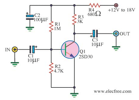
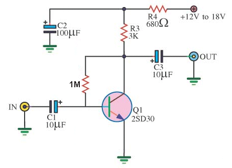
This PRE-AMPLIFIER circuit will not turn ON because the voltage on the
base is 50mV and it should be 650mV.
The voltage-divider resistors on the base are incorrect. The 4k7 should
be at least 47k.
Using the correct ratio of base resistors will turn the transistor ON
but the actual voltage on the collector will depend on the gain of the
transistor. Using 3 resistors in a semi-bridge arrangement is not a good
idea. It should have an emitter resistor bypassed with a 100u
electrolytic.
It is much better to use a self-biasing stage as shown in the second
diagram to produce approx mid-rail voltage on the collector.
![]()
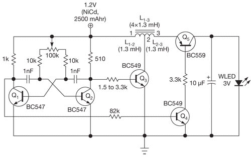
I have never seen a more-ridiculous circuit in all my life. Apart from
being over-designed, it contains a number of technical faults.
A BC549 will not pass more than 100mA at the best of times and in this circuit
the base has a 2k resistor so the current is limited to less than 100mA. It is
not a "power transistor" and has no current-carrying capability. Maybe a BC338
with 1amp capability is a better choice.
The charging-current through the inductor is an indication of the energy that
will be available when the transistor is turned off and in this circuit the
charging-time can be adjusted.
You only need to allow current to flow through the inductor until it is
saturated. Any further current-flow is wasted. It is impossible to determine
this without accurately measuring the flux produced by a totally isolated
secondary winding. And this feature is not available in this circuit.
See our Joule Thief article for correctly-designed driver circuits.
What is the point of transistors Q4 and Q5? They serve NO PURPOSE. They
simply turn ON and allow energy to flow to the 10u and LED. You cannot pass all
the energy from the inductor by simply adjusting the mark-space ratio when you
are using the same adjustment for the "charging operation." It just needs a
high-speed diode to pass the energy.
The inductor is overly complex. If you turn off the transistor quickly, the back
emf (high voltage) produced will be sufficient to drive a white LED. You don't
need and extra winding.
The 510 ohm resistor on the collector of one of the multivibrator transistors
means current is being wasted for part of the cycle.
The driver transistor should be "driven" by a previous stage and not simply
"pulled high." What the designer has done is analogous to turning off a car's
headlight by shorting across the battery.
The characteristic voltage-drop across a white LED is between 3.3v and 3.6v. He
suggests 3v and it indicates he has not driven the LED to its capability.
He has used a 1 watt LED and delivered 30mA.
The 10u across the LED has very little effect as it gets charged to 3.6v and
when the voltage drops to 2.8v, the LED is not illuminated. This small amount of
energy from a 10u will hardly be noticed.
The designer claims the output of the multivibrator is triangular, whereas a
multivibrator is known as producing square waves.
The circuit below turns ON the transistor HARD to produce the highest output.
The circuit above turns on the transistor very feebly and it will have a high
collector-emitter voltage that represents wasted energy.
There is no point in having a tapped inductor. By driving the transistor
correctly, a single inductor will produce sufficient voltage to drive the LED.
The inductor used in the circuit is expensive ($5.00) and a simple hand-wound
coil could be used.
Overall a badly-designed circuit that is overly complex and very inefficient. A
good study in "how NOT to design a circuit."
When you see a simple single transistor circuit that performs the same function, you realise how stupid to try and guess the timing to "charge" the inductor. The following circuit does it automatically and by simply changing the number of turns on the transformer (and its size), you can increase the output. See the Joule Thief article for more details and a circuit using a transformer with an AIR CORE !
![]()
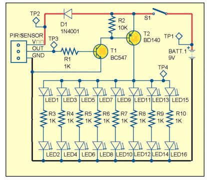
WET NAPPY ALARM
The main reason we included this circuit is due to the layout.
It is impossible to work out what the circuit is doing. The layout is just a
jumble. The circuit is presented in the May issue of Electronics For You
Magazine and is supposed to cater for beginners to show how a circuit
works. I have no idea what the circuit is doing. How do you expect a beginner
to learn from this layout ????
Here is the correct way to layout a circuit so the operation of each "building
block" can be understood:
Each NAND gate is a 2-input Schmitt Trigger with the first gate wired as an
inverter. The second Schmitt inverter is a high-frequency oscillator and the
third gate is a low-frequency oscillator. These two oscillators are gated to the
fourth block to drive a piezo diaphragm as beep-beep-beep.
A 1k on the output is not needed and will only reduce the loudness of the piezo.
![]()
LED LAMP
Here we have the ridiculous situation of providing isolation via a transformer
but producing the dimming feature via a rotary switch on the MAINS SIDE of the
transformer.
The same switch could be placed on the secondary side with smaller wattage
resistors to produce a much-saver circuit.
The purpose of the two 100 ohm resistors, 100n capacitor and 150mA fuse is
unknown. [150mA fuses are very unreliable and when they are a slo-blo type, they
do not burn out until 500mA flows.]
These items are not needed. The power lost in R2 is less than 5mW - why
use a 2 watt resistor ????
The 10 ohms resistors are far too small to have any effect. We have already
discussed using a low-value dropper resistor in series with LEDs in our
30 LED Projects
eBook.
The whole circuit is badly designed and gives the wrong information to newcomers
to electronics.
Sani Theo, the technical editor, doesn't know what he is doing and is just
making a fool of himself and Electronics For You Magazine.
This is another stupid design from Electronics For You Magazine May 2013
issue.
When you are designing a circuit, you need to "THINK OUTSIDE THE BOX." This
involves looking at the circuit and seeing if it can be improved. The circuit
above is a typical example. It would not be accepted in Australia, where the
rules for transformerless power supplies, switching the mains via rotary
switches and, in fact, anything to do with power supplies, dimmers, battery
chargers etc is tightly regulated and prevented from publication in hobbyist
magazines.
The rotary switch should be placed on the secondary side of the transformer
where it will be perfectly safe to handle and the circuitry will be simpler.
![]()
WATER TANK PUMP
Here's another absurdly over-designed circuit:
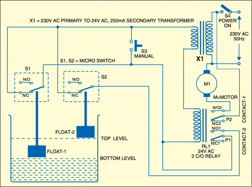
All that is needed is a float with a pin at the top and bottom that moves the
lever of a toggle switch. When the float falls it turns the pump ON and when it
rises, the pump is turned OFF. The float can be a plastic Coca Cola bottle
partly filled with water. A plastic pipe in the top and two pins to touch the
switch. The pipe will need guides to all it to rise and fall.
This is another over-design from Electronics For You Magazine where they
didn't "THINK OUTSIDE THE BOX."
![]()
MINI UPS
The 12v battery will drop 0.6v across D4 and a further 2v across
the emitter-collector of the Darlington transistor T2. The output at "A" will be
less than 9.4v and not 12v.
The 9v regulator will also drop out of regulation as it needs at least 2.5v
across the IC.
This circuit is a failure as a back-up power supply.
What is the purpose of D3 ??? It is not needed.
The FULL CHARGE LED will come on slowly and not give an indication of the
exact point when the battery is charged.
What is the point of ZD1, the 22k? (20k) pot and T2 when the output has
a regulator and 12v zener.
The whole circuit does not make any sense.
![]()
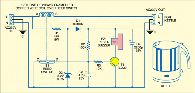
More Junk circuits from Electronics For You website:
This circuit detects when the kettle turns off. But the 47k will only provide
about 2-3mA for the piezo buzzer and they require 10mA to 20mA.
The reed switch will be vibrating at 50Hz during the 5 minutes when the water is
heating and this will eventually break the reed. They do not last very long.
Each heating will create 15,000 vibrations.
Why have 2,200u to collect 3mA !!!
Just another JUNK circuit that has not been tested.
![]()
This is a STUPID CIRCUIT:
If you push the wrong button you are not penalised. Simply push each button (in turn) 7 times and the lock will open.
![]()
ALARM
Here's another circuit from Professor D. Mohankumar
email:
mohanwordpress@gmail.com that does not work.
The output of the op-amp goes LOW to turn on the buzzer. But the LED is around
the wrong way and the transistor is an emitter-follower so that the buzzer will
get less than 6v due to the voltage-drop across the LED, the base-emitter
junction of the transistor, the drop across the 1k and the output of the 741
being slightly above the 0v rail.
He does not test ANYTHING !!!!!
![]()
MULTIPLEXING
Here we have a typical multiplexing arrangement where a microcontroller drives a
4-digit display.
Each display is accessed turn and it only gets turned on for 25% of the time.
However you eyes have a feature called Persistence Of Vision (POV) that retains
a previous image for a fraction of a second after it has been removed, so that
the whole display will appear to be illuminated.
However to get a good brightness from the 4 displays, you have to drive them at
10mA to 15mA. The chip is only capable of delivering 10mA per output and it is
really not suited to directly driving a display like this.
But when dropper resistors are included the drive-current decreases to a point
where the display is almost useless.
That's the case in this example. The LEDs drop 1.7v, the sourcing
transistor drops 0.6v across the base-emitter junction and the micro has 0.3v
between output and 0v rail. This means the dropper resistors have 2.4v across
them.
The 10k base resistor can be divided by 100 (the gain of the transistor) and
included as a 100 ohm resistor. This means the dropper resistors equal 430 ohms.
The maximum current that 2.4v can deliver via 430 ohms is 5mA. The displays will
be very dull.
The emitter-follower used to drive each display should not have a resistor on
the base. This transistor should be turned ON-FULLY so the 330 ohm resistors can
provide the current limiting.
A very poor design with a number of faults.
![]()
FRIDGE ALARM
This circuit comes from Future Kit, a Thailand based kit company. The component values do not matter as you can see the fault in the circuit by following this explanation:
When no light falls on the photo transistor, it resistance is very high, the
voltage on the base of TR1 is less than 0.6v and the transistor is turned OFF.
Capacitor C1 is charged via R3 and D1. This puts a voltage on the base of TR2
and the transistor is turned ON.
Full rail voltage appears across R6 and thus the voltage on the base of TR3 is
less than 0.6v and the transistor is not turned on.
All the rest of the circuit is not active.
But a small current flows through R3, D1, R4, VR1, R5 and R6. This is an absurd
way to turn off a circuit.
It's a bit like putting a short-circuit across a battery to turn of a globe or
motor.
The circuit is effectively putting a short-circuit across the input of the
switching transistor TR3 to keep the circuit OFF.
Here is a simpler circuit that takes NO CURRENT when the LDR does not detect
illumination:
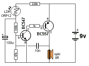
This circuit drives an active piezo buzzer and the circuit takes no current when "sitting around."
It will start to produce a sound about 15 seconds after the Light Dependent Resistor detects light.
The mini piezo buzzer contains a transistor and inductor to produce a high amplitude oscillator to drive the diaphragm and produce a loud squeal from a supply of 3v to 5v. It will not "turn on" from a slowly rising voltage so the circuit must be designed to rise rapidly when light is detected. That's the purpose of the 2nd and 3rd transistors. They form a high-gain amplifier that rises quickly due to the positive feedback provided by the 100n.
As soon as the second transistor starts to turn on, it turns on the 3rd transistor and the collector voltage rises. The right-plate of the 100n rises and since the 100n is uncharged, the left plate (lead) rises and increases the voltage and also the current into the base of the second transistor. This makes it turn on more and the action continues very quickly until both transistors are fully turned on. They stay turned on by the voltage (and current) provided by the first transistor.
Even though we normally see the second two transistors used as an oscillator, we can use the "rapid turn-on" feature to "kick-start" the piezo and if the middle transistor is provided with too-much voltage (current) on the base, the oscillator feature will not occur because the current into the base is too high and the 100n cannot remove this current during the turn-off period of the cycle. The only unusual feature of this circuit is the oscillator section starts to oscillate at very low amplitude when the first transistor turns off (when the LDR ceases to be illuminated) and a 10u has been added to stop this oscillation so it takes no current when at rest.
![]()
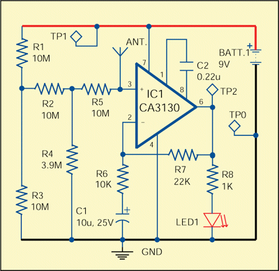
Electronics For You is still publishing circuits that do not work:
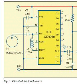
An inverter is contained inside the chip, between pins 11 and 10 with the input
on pin11. When an inductor is placed between these two pins, an oscillation is produced and the frequency is determined by the delaying action of
the inductor. But the inductor has a lot of "strength" in delivering this
signal, (because the inductor has a very small resistance) so that if a finger is placed on pin 11, the amplitude of the signal is
not decreased.
For a TOUCH PLATE to work, the signal must be very weak and only just able to be
detected by the input of a chip. When a finger is placed on the plate, the
signal is absorbed slightly by your body and the input registers "no signal."
This circuit has been tested and DID NOT WORK. Another Electronics For You
failure.
Try 10k to 100k in series with the 100uH inductor. (You need to make the
oscillator-pulses very weak so your finger will reduce the amplitude.)
![]()
Another Electronics For You circuit that does not work:
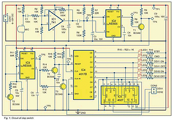
Apart from the circuit being far too complex, the circuit contains a major
fault.
Here is the response to your claps:
Two claps: Turn Device 1 'on'
Three claps: Turn Device 1 'off
Four claps: Turn Device 2 'on'
Five claps: Turn Device 2 'off
The designer of the circuit failed to mention the fact that you cannot keep
device 1 ON and turn ON device 2, because the output sequence of the 4017
controls the flip flops in the 4027 IC and as the pulses pass the flip-flop that
controls device 1, the flip-flop is RESET (as the signal passes to the flip-flop
that controls the second device).
On top of this, you need a lot of claps to perform a simple task.
A really messy design that DOES NOT WORK !!!
You can see a simple design using a microcontroller on our new website:
Electronics Maker
![]()
DOOR ALARM
Here's a Door Alarm circuit that does not work.
The circuit takes 1mA when sitting around
due to the 10k resistor feeding the reed switch and the output of the circuit (pin
11) goes HIGH when the alarm is not producing a tone and this turns on the
transistor and causes a high current to flow in the speaker. The battery
will go flat in an hour.
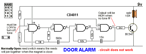
It is impossible to work out the state of the gates when a block diagram is
presented and all circuits should be drawn with gates, so you can see what is
happening. The next circuit is drawn with gates, so you see the mistakes.
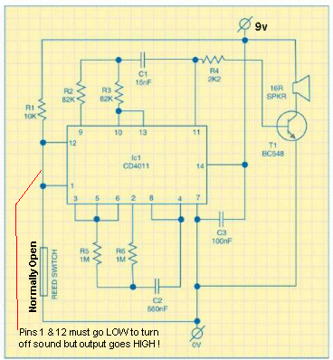
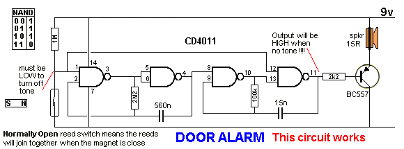
By making a few changes, as shown in the circuit below, it consumes less than 10
microamps when "sitting around."
Two resistors have been removed as they are not needed. The 10k has been
replaced by 1M and the BC547 has been replaced by BC557.
![]()
Another Electronics For You badly-designed circuit, July 2013:
When the 22k mini trim pot is turned fully clockwise, the 9v supply will be
directly across the FET inside the microphone and will possibly blow it up.
![]()
Another Electronics For You badly-designed circuit, July 2013:
Apart from the fact that the layout of the 7805 and driver transistors for the 3
digits on the display are all up-side-down and hard to follow, the PNP
transistors for the display are badly configured. The drive-lines to the display
should contain 220R resistors (7 x 220R) and the BC558 transistors should have
no resistor.
The problem with the circuit above is this: As more segments on a particular
display are illuminated, a higher current will flow though the 220R resistor and
create a larger voltage-drop. This means the segments will get duller as more
segments are illuminated.
The second poor design is the connection of the base of each driver transistor
to an output of the microcontroller.
This arrangement is absurd, as a low on the base of each transistor will fully
turn it on and not allow the current to pass to the segments of the display. I
don't know how they expect the circuit to work. It has obviously never been
tested.
The next problem is the value of R11. The circuit suggests 15R. And the parts
list suggests a 5watt high-power LED.
Let's go through the mathematics. If you have a supply of 16v DC from the
rectification of the 12v - 0v - 12v transformer, the voltage across a
5watt LED will be about 3.6v. This leaves 12.4v across the 15R resistor and thus
825mA will flow. This gives the LED .825 x 3.6 = 3 watts. The wattage lost in
the 15R resistor will be 12 watts!!
If you put two LEDs in series, the result will be: 3.6v + 3.6v = 7.2v The
voltage across the 15R will be 8.8v. The current will be 590mA and the wattage
will be 8.8watts The wattage of the LEDs will be 4.2watts. Obviously the
values provided by the author do not work.
It is not good enough in the text to say: "select your own resistor."
You need to
provide details on how to select the value, especially when a high current is
involved.
![]()
Another Electronics For You badly-designed circuit, July 2013:
This circuit contains 4 separate paths that will create a high current. We have
shown one path consisting of semi-conductor junctions (with NO current-limiting
resistor) and these junctions have a very low resistance when conducting. This
means a very high current will flow and even though two of the three transistors
are fully turned ON to drive the motor, the current-flow will be higher than
required because no CURRENT LIMITING resistor has been included in the circuit.
The current can be high enough to damage the transistors. This is a MAJOR fault.
![]()
Another Electronics For You badly-designed circuit, July 2013:
A protection diode is needed across the 7812 regulator to protect it from
reverse voltage when the 12v battery is connected and the power from the mains
is not present.
The 1,000u capacitor will be uncharged and the voltage on the output of the 12v
regulator will be 12v when the battery is connected and may cause damage to the
regulator. This 12v-difference may damage the regulator but if a 1N4004 diode is
added, the voltage-drop across the diode will be only 0.7v and the regulator
will be protected.
![]()
Another Electronics For You badly-designed circuit, July 2013:
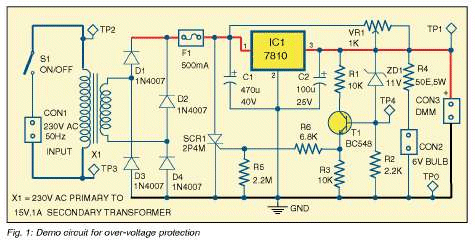
The circuit above detects an over-voltage and trips an SCR to blow the 500mA
fuse. This is a drastic way to save an over-voltage condition and is called
"CROWBAR PROTECTION."
In 40 years I have never heard of a voltage regulator failing and producing an
over-voltage, even though I have sold thousands of power supply kits and
thousands of computer kits using a 7805 regulator.
So I think the circuit is solving a problem that does not exist.
However, apart from this, lets look at the circuit and see the bad design
features.
Firstly, a 7810 regulator is very unusual. If you re going to produce a "general
circuit," the components should be commonly-used values.
Secondly, the 15v transformer will deliver 20v to the regulator and this will
produce 10 extra volts across the regulator. At 500mA this amounts to 5watts.
This could be the cause of the regulator failing.
The 1N4007 diodes should be specified as 1N4002 or 1N4004 as 1N4007 are 1,000
volt diodes and are only specified when voltage spikes can be of this magnitude.
Now we come to the BC548 transistor. What is the function of this transistor? It
is not needed. The zener can be connected directly to the gate of the SCR,
saving 4 components.
The following circuit switches off the output when the voltage from the
regulator rises above a specified value and reconnects when the voltage falls.
The voltage will rise if the bottom terminal of R2 is removed from the 0v rail.
![]()
Another Electronics For You badly-designed circuit, July 2013:

This is a very dangerous circuit. The output voltage will jump to 12v when the
switch is moved from 3v to 5v.
DO NOT BUILD THIS CIRCUIT.
The switching should be between the adjust pin and output.
![]()
Another Electronics For You badly-designed circuit, July 2013:
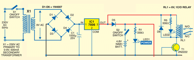
There is no current limiting resistor when charging the NiMH battery from the 6v
regulator and the charging-current will be unknown.
NiMH batteries are very complex to charge and a simple charger like this will
cause damage.
NiMH cells should not be charged above 1.78v per cell (5.25v total) and this
charger will keep charging as the input voltage is 5.4v. Just a very
dangerous circuit. Do NOT build this circuit.
![]()
Here is a technical reply with lots of mistakes:
I have a 1.5 watt solar panel battery charger. In full light it registers
around 14+ volts and at least 1.5 watts. I would like to use this panel to power
a small dc motor that I pulled from a portable CD player to use in a science
fair project for my son. Whenever I hook up anything to this, it seems to drain
all the power from the panel and does not power the motor. How can I figure out
what I need to power a dc motor that typically runs off of 2 1.5vAA batteries
(3v or less power).
I'm guessing the solar cells aren't big enough. -
The motor probably pulls very little power with no load on it. I assume the motor you're trying to use is from the tray mechanism, it is a DC brush motor, not a stepper motor. There is no tray mechanism on a 3v portable CD player. The motor the enquirer is using is a STEPPER MOTOR that spins the disc.
The spindle that spins the CD is usually a brushless synchronous motor, not something you just put DC on and it runs. The motor that runs the tray to eject the disk is probably a simple DC brush motor. There might be a third motor that moves the head back and forth, that is also usually a DC motor. You want to use one of these DC motors. These motors will probably run on 3V but pull right around 1.5W. No 3v motor requires 500mA - 1.5watt. A 3v motor normally requires 70mA to 170mA.
So they might not run unless you have full bright sunlight on the solar cells. Another issue is if you have solar cells that are made to charge batteries, they are probably not made to supply very much current, they are wimpy little things. Still, 1.5W at 14V is around 100mA, that might still be enough to run one of these motors. Try this - if you have a voltmeter that measures current No voltmeter measures current - Shilpo Kapoor should say "Multimeter."
connect it in ammeter mode right up to the two wires from the solar panel. That will put a dead short on the solar cells (an ammeter is always a short), but it will measure the short circuit current of the panel, and won't hurt the panel at all. Try it with indoor light, then sunlight. Put the meter on like a 200mA full scale mode. If you put the ammeter on 20mA full scale you might damage the meter in full sunlight. If you really want to be safe, use the meter's 10A scale first to see what range the current is. If the current reads like 10mA, it will never get the motor moving. If it's 100mA, it will probably try to run the motor, if you spin the motor you will find it wants to go one direction and resists going the other direction. You can also power the motor from 2 batteries and measure the current it is pulling while running.
Shilpo Kapoor, Lotur
You cannot connect a 3v motor to a 14v solar panel. As soon as you get a small amount of sunlight on the panel, the motor will "over RPM" and the armature windings will possibly be damaged.
![]()
Another Electronics For You badly-designed circuit, August 2013:
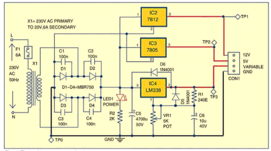
This project has been submitted by ABHISHEK KUMAR a final-year student with
absolutely no electronics experience AT ALL.
The rubbish he is presenting is passed to 50,000 readers of the magazine and
many will experience problems with the power supply.
Let's look at the first problem. When a transformer states 20v AC secondary, the
voltage will be 20v at full load. All transformers have a term called
REGULATION. This means the output voltage will be slightly higher than 20v when
the current is say 1amp, because the as the current increases, the resistance of
the secondary winding will cause a slight voltage-drop. This means the no-load
voltage will be about 23v to 25v.
The author states the output voltage will be 28.2848 volts after the rectifier.
What an absurd thing to say when the AC voltage can be anything from 20v to 25v.
You cannot state an accuracy with more figures than the given data.
If we take the 7805 and try to draw 1 amp, the voltage across the 7805 will be
25 x 1.414 - 1.4v = 34v - 5v = 29v.
Wattage dissipated as heat will be 29 watts.
The regulator is designed to allow a maximum of 15 watts to be generated as heat
and this means the regulator will only allow 500mA load.
The same applies to the 7812, with about 700mA load. I am not going into the
finer details because the circuit is so badly designed that I would not
construct it.
For the LM338, the situation is just as bad. The metal-can version of the regulator can dissipate up to
50 watts, and this is just like the heat of a soldering iron. 50 watts is a LOT
OF HEAT! The plastic version (as shown on the diagram with leads marked 1,2,3)
dissipates a maximum of 25 watts.
Suppose you adjust the LM338 to output 10v at 5 amps. This will produce 20 x
1.414 - 1.4 = 26.8v -10v = 16 x 5 = 80 watts. The chip cannot
deliver more than 3 amps due to the badly-designed power supply.
The output of a regulator should have a 100n and 10u electrolytic to prevent
parasitic oscillations (1MHz oscillations). These capacitors need to be close to
the regulator to have any effect.
None of this has been considered by the author or the Technical Director of the
magazine Sani Theo.
I have repeatedly told Sani Theo to contact me before publishing rubbish
like this, but he doesn't have the intelligence to get these circuits analysed
before publication and continues to deliver this rubbish to the readers of the
magazine.
![]()
This circuit has been produce by Dr D.G. Vyas. The states he is in-charge head, department of Physics and Electronics, Hem. North Gujarat University, Patan
He has no electronics knowledge AT ALL.
You cannot connect a transformer to a battery and expect it to charge the
battery without overcharging.
But most-important, you cannot connect a transformer to a battery as the
transformer will BURN OUT.
The circuit above is one of the worst circuits I have seen. It does not matter
if you are a Doctor, Professor, or student, test and check your circuit before
sending it to a magazine, where lots of intelligent readers will see the
badly-designed circuit.
Here's the point that no-one has mentioned before. A battery is just like
a zener diode. It sits in the circuit just like a 15v zener diode when it is
fully charged.
If you have a transformer capable of delivering more than 15v, current will flow
into the battery. Just because the transformer is rated at 500mA, DOES NOT mean
that 500mA will flow. A lot more than 500mA will flow and the actual
current-flow is unknown, but will depend on the resistance of the secondary
winding. It could be as high as 1 amp or 2 amp and the transformer will
definitely BURN OUT.
No only will the transformer get very hot and eventually burn-out, but the
current into the battery will not reduce when the battery is fully charged and
it will start to "gas" and dry-out very quickly.
You MUST have a voltage regulator to supply the exact voltage when charging a
battery or deliver a trickle charge so the battery will not "dry-out." None of
this was mentioned in the article.
The remainder of the project uses 7-segment displays that are not carried by any
parts-supplier. Obviously the author has dug up some "junk bits" without making
any effort to see where they can be purchased.
I'm glad Dr D.G. Vyas is not my lecturer.
![]()
Another Electronics For You circuit with mistakes, August 2013:
![]()
D4 should be reversed and D1, D2 are not needed:
![]()
When designing a circuit, ask yourself this simple question: Is this component needed? remove the part and see if the circuit works. The combination of D1 and D2 will pass current, no matter if the polarity of the supply is positive or negative. Thus they are not needed. Another untested circuit from Electronics For You magazine.
![]()
Edge FX wanted me to recommend their site and provide a link.
Look at just one of their kits. A voltage multiplier:

Look at the bare connections at the end of the 240v power lead !!!!
Look at the 1,000v diodes soldered on top of each other !!!!
The kit contains 100u electrolytics. Can you imagine the current that can be
supplied by the multiplier circuit !!!
It looks like the electrolytics are connected in series. Why ??? You
can get 100u @ 415v
The kit costs $289 !!!!
Now have a look at where they are reading the output voltage !!! They have
the voltmeter connected to the 2,000v end of the generator !!!!
The voltage divider consists of 10 resistors to divide the 2,000v to produce
200v across a single resistor but they are reading the HIGH END and not the
"EARTHY END" !! The voltmeter will have 2,000v on it !!
Edge FX has NO IDEA how to design a kit and this kit is one of the
worst, MOST DANGEROUS kits on the market.
You can imagine why I didn't recommend their site.
![]()
Here is another absurdly over-deigned, over-priced ($219) design from Edge FX:

The circuit is designed to increase and decrease the brightness of the LEDs. The
LEDs are supposed to be a lamp, but they are next to all the extra circuitry and
the project is not very practical.
The 8051 microcontroller is HUGE. All the project needs is an 8-pin PIC micro.
The LEDs have only a single current-limiting resistor. This is a BIG MISTAKE.
Very poor design.
The current limiting resistor is a very low value and this gives the circuit a
very small supply-voltage HEADROOM. This is something the designer knows nothing
about.
The text does not say if the project is operated via a timer to raise and lower
the brightness of the LEDs according to the time of day or if a photocell is
included to adjust the illumination. Since there is only one input and one
output, a very small micro is needed.
Just another JUNK project with very poor design-features and a price that would
scare almost all electronics engineers.
If you can't produce a project like this for $20.00 or less, you are in the
wrong market. No-one is going to buy a lamp for $219.00
They are trying to sell their projects to desperate final-year
electronics engineers who can't design their own project. They think EVERYONE'S
a FOOL.
![]()
Here's another ($229) design from Edge FX:
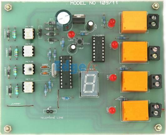
It connects 4 parallel phones to the phone line and only allows one phone to receive the incoming call. The circuit has been copied from a project on the web and the mistakes in the circuit have been copied without any corrections. Note the 220k across the LED on the opto-coupler. It should be 100R
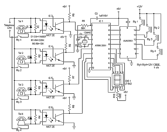
It is not obvious from the diagram, but the relay contacts are normally closed
so that all the phones are on the phone-line when the incoming signal (ring
signal) is received. This is an AC signal and will not have sufficient current
to illuminate the LED in the opto-coupler.
When one phone is lifted, the corresponding LED in the opto-coupler illuminates
because the phone draws the phone line down from 50v to about 12v and takes
about 20mA to 40mA. The resistor across the LED should be about 100R so that
some of this line-current flows through the resistor.
The transistor in the opto-coupler turns on and produces a LOW on the
corresponding input to the microcontroller.
The micro turns on the other three relays so that other phones are removed from
the phone-line.
When the phone is put down, the relays are de-energised.
The project above has LEDs corresponding to each relay and there is no need for
the 7-segment display.
This circuit can be created with gating diodes and a few components. Here is the
circuit:
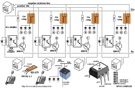
See full details on: http://www.electronicsmaker.info
![]()
Page 1
Page 2
Page 3
Page 4
Page 5
Page 6
Page 7
Page 8
Page 9
Page 10
Page 11
Page 12
Page 13
Page 14
Page 15
Page 16
Page 18