|
FAULT |
I have to tell you, my enormous knowledge of circuit design came from my servicing experience, over 20 years, where I fixed and improved faulty designs and found their limitations and mistakes.
This is called REVERSE ENGINEERING or REVERSE LEARNING and is by far the most accurate, fastest and most intelligent way to learn. Students learn a whole year-course in weeks.
You have got to remember this: Nothing the instructor says, makes any sense. After reading this article, you will agree.
oooooooooooooooooooo00000000000000000000000ooooooooooooooooo
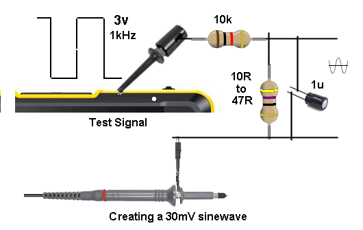
The only way to work on audio equipment is with a CRO. With the cost of these pieces of test equipment falling to less than $60, there is no excuse for not having one "in your pocket,"

This is the one I purchased from Aliexpress and it
arrived in a week.
It will take some time to learn all the features and we are not going
into the lessons for setting up the screen, but to say you need the
probe and make sure the switch on the probe is set to X1.
The DSO has a 3v test point that produces a 1kHz square wave on the top
of the case and you can convert it to an "AC waveform by connecting 100R
to the test point and placing 1u on the other lead of the resistor.
Connect the negative of the 1u to the earth clip of the probe with a
long lead. You can put attenuating resistors on the output such as 10k
and 1k to get 100mV or 100R or 47R to get 10mV. This DSO produces a test signal
of 3V.
This is all you need to work on audio projects.
Voltages don't tell you anything at all. You need to know if the signal
is being distorted or clipped at each stage of the progress through the amplifier. You need to
look at the amplitude of
the signal, as clipping will be due to your test signal having a high
amplitude and changing the shape of the signal will be due to the
selection of the components. The DSO has its own internal battery so there will not be any earthing or power supply conflicts.
The first thing you do is start at the front end and look at the signal.
Clip the test lead to the input and see if the amplifier changes the
amplitude or shape of the signal or any sort of hum introduced into the
signal. That's why it is best to keep everything on batteries.
You can use mini trim pots for attenuation for the attenuation of
signals in place of resistors.
This will give you some idea of the impedance of the input signal.
If the real signal is being generated from a coil or inductor, it will have a
very low resistance, but it will also have a very small current
capability and that's why the input impedance of the circuit must be
high.
Input signals can be as low as 1mV to 10mV so you must match this amplitude
when designing a circuit otherwise it will "over-drive" the amplifier.
As you move along each stage, the signal will get larger and not fit on the screen
and you will have to change the SENSITIVITY.
This is to do with the "input voltage."
The highest sensitivity of the DSO is 10mV/division.
A "division" is the lines across and up and down on the screen.
These are called SCREEN GRATICULES
There are 10 divisions to the height of the screen so that in the most
sensitive mode, the screen will show a signal 100mV high (amplitude).
The wave on the screen is actually a dot and is called the TRACE.
The amount it rises and falls is called the EXCURSION or AMPLITUDE.
The maximum frequency that can be processed by these low-cost DSO's is
about 100kHz to 200kHz. This is way above the frequency you will be
detecting.
Looking at the test wave does not give you any idea of the quality of
the audio you will be passing through the amplifier.
You need to listen to the audio with a Mini Bench Amplifier as the sound
may be "hollow" or only picking up close sounds.
That's why all audio needs to the monitored with head-phones.
The most difficult circuit to analyse is the 4 to 6 transistor DC
coupled arrangement. All transistors are connected to each other
with resistors and no capacitors are used.
There is a feedback line to the front-end that sets the operating-point
for all the other components.|
Since the is no "starting point" for diagnosing this type of circuit, it
is best to replace all the transistors.
There are a number of "hum" and instability problems with amplifiers.
Background 100Hz or 120Hz hum can be due to power supply electrolytics
or even one of the bridge diodes in the power supply.
A slightly different background sound called MOTORBOATING is due to
interstage-decoupling electrolytics.
Electrolytics generally last about 20 years but any amplifier used
outdoors in the heat will give them a limited life.
Forget everything you have seen or been told or viewed at a lecture or on YouTube, about designing an H-Bridge amplifier.
Simply buy a $50 Digital Storage Oscilloscope and build the circuit yourself and see "how and why" it does not perform anything like what you have been told.
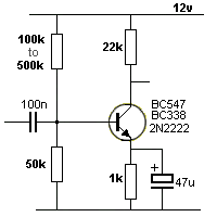
Use the circuit above and the circuit below to create a 30mV sinewave (1kHz) for injecting into the test amplifier above. Some DSO models have an output test signal of 3v or higher and you need to use amplitude-dividing resistors to suit your signal and bring it down to about 20mV to 30mV..
CAUTION
As you select different input "sensitivities," the amplitude of the signal on the screen will change. This is because the DSO is putting a different load on the signal and attenuating it.
For instance, the output was measured as 5v on a 5v setting, but when the input sensitivity was changed to 10mV per division, the peak-to-peat amplitude was only 500mV, so you are not getting a true reading when you are measuring an amplitude in a part of the circuit that is classified as HIGH IMPEDANCE.
This a whole new topic to learn about, and has never been covered, and that's why you need an enormous amount of skill to interpret reading on the screen of a low cost piece of test equipment.
When you build the circuit you will find the amplitude
of the signal on the collector will be about 1v, no matter which
transistor you use.
You will also find the top base biasing resistor can be from 100k to
500k and the output does not change.
On top of this the 50k lower resistor can be reduced to 30k or removed
without any change in the output signal.
We also shorted across the 1k emitter resistor and the output did not
chane.
Three different types of transistors were used with the same results.
They had a measured DC gain of 260 to 300.
We also measured the signal on the base and found 20mV produced the same
amplification as 30mV input.
With 20mV input ad 1,000mV output, the gain of the stage was 50 and this
was about the maximum and did not change by any noticeable amount when
all the other alterations were made.
The conclusion is obvious. It is pointless getting involved in any sort
of mathematics and component values when a whole range of values will
produce the same results.
You are just being hood-winked and fooled into learning about designing
a stage when the transistor does not behave any like you are told. The
transistor have a gain of 150 to 350 and the stage is taking less than
1mA so it is classified as a low current stage. None of the facts,
figures, load-lines or transistor data is supported in the final
operation of the circuit and so you should really be taught what is
happening with the stage.
For a start, the base bias resistor does not need the lower resistor and
the current through the biasing resistors certainly does not have to be
10 times the base current.
I don't know where the instructors get this stupid determination from.
The base bias resistors do not form a VOLTAGE DIVIDER. (the 10 to 1
concept only applies to a Voltage Divider)
All the biasing resistors need to do is deliver a voltage that starts to
turn the transistor ON. The energy coming from the input capacitor does
all the rest of activating the stage.
The same with the emitter resistor. You can short across this resistor
and the output amplitude does not alter.
That means the emitter resistor and electrolytic do nothing.
Finally, when the 250mV square-wave test signal is injected into the
amplifier, the output is a 1v square wave at 1kHz and changing the input
capacitor from 100n to 1u or 10u made no different.
So, what is the secret. The secret is to use a single, very high
-value, base resistor that just turns the transistor ON, so the
quiescent current is between 0.1mA and 1mA.
Because the base resistor is connected to the positive supply rail, the
gain of the transistor in static mode will determine the quiescent
current and this will alter and control the collector voltage
enormously. .
And since the emitter resistor and electrolytic, are not needed, the
circuit becomes very similar to the self-biased stage.
If you want the stage to automatically sit at half-rail voltage, you can
connect the base resistor to the collector and it become a self-biased
stage.
Changing the 22k load resistor to 10k or 1k did alter the output spade
and amplitude considerably buy we will not be covering the change as as
it is a discussion for another time.
None of the instructors have alerted you to the problems and flaws and
mistakes and limitations of the H-Bridge because they have never done
and experimenting, testing designing or research into the validity of
what they are scribbling on the white board.
None of them have ever said the transistor will behave completely
differently to what they are predicting from the data and you don't have
a change of succeeding in this area.
I am not saying that all the things I am stating will apply to all
H-Bridge circuits at all voltages and loads.
What I am saying is the fact that you cannot deign this type of circuit
"on paper" an expect it to work. The reality is completely different and
you need to build the circuit and deliver the input signal from an
actual device and connect the actual load you will be using. All the
data I have provided had NO LOAD connected to the circuit and when you
connect a load, things will change again.
But you have to start in the right direction. Get on the right
"tram" and realise you must do things in a practical way, as this is the
only way to gain success. All the other ways are "speculative" and
"wishful thinking."
You are wasting your time designing a stage with mathematics. You are also wasting your time designing with a DSO.
As you change the value of components you can see the shape of the output change. But you don't know how this is changing the audio. It can make it "harsher" distorted, "tinny" or "clipped."
The only way to design an audio stage is to use an electret microphone to pick up room noise and wear a set of headphones to hear the effect of changing the value of the components.
All the self-biased stages I designed for FM bugs were designed in this way and the audio from the transmitted signal was so accurate that the sound from the radio in the next room made the staff think I was in the next room.
When you boil down all the hype of the H-Bridge and compare it the self-biased stage, you will find the self-biased stage is the best design for a pre-amplifier or a very low current stage.
The H-Bridge arrangement can be used for the next stage in an amplifier where currents from 1mA to say 10mA are involved.
QUESTIONS
Here are some questions for your instructor for an H-Bridge circuit.
Why is the bleed-current for the base resistors 10 times the base current?
The bias resistors are NOT a voltage divider and the principle of voltage division does not apply.
The biasing resistors are attenuating the input signal for no purpose.
Why use two resistors to bias the base of the transistor, when a single resistor of a higher value will achieve the same result, in conjunction with the emitter resistor.
Why do you require the transistor to sit at mid-rail, when the energy from the input capacitor will immediately take over and drive the transistor with much more force than the biasing current and fix any situation where the transistor is at almost "cut-off" or almost "bottoming" due to faulty biasing.
Why be so specific with the value of the input capacitor when almost value will produce the same results and you do not know the results until you compete the design and view the waveform.
Why design a circuit without including the value of the output LOAD as it will alter the signal enormously.
Why not design an H-Bridge circuit and then a self-biased stage with just 2 components and compare the results.
THE COMMON BASE
AMPLIFIER
No-one has described the Common Base amplifier.
It needs a bit of understanding and the following circuit takes the
output of the Common Base stage and increases the current-capability by
about 100 times. It takes two stages to do this.
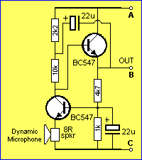
The Common Base stage will
accept a very low impedance device between emitter and 0v rail and
deliver an output on the collector.
The transistor does not produce any amplification.
The way it works has never been described before as no-one has
understood how the circuit works. It is the surrounding components
that "create" or "generate" the "effect" and the effect in this circuit
is to produce a voltage increase of 1,000 and a current increase of
about 300. We know a transistor does not have this much gain and
so we need to see how the circuit works.
We start by turning the circuit ON.
Neither transistor is turned ON and especially the lower transistor as
it has a 22u on the base and this will take time to charge.
The lower transistor, speaker 1k and 22u are "out of circuit" and the
top transistor is an EMITTER FOLLOWER and the base is pulled HIGH by the
10k and 2k2.
This pulls the 4k7 HIGH and the 22u starts to charge.
As soon as the base of the lower transistor sees 0.55v, it starts to
turn ON and reduces the 10k's ability to turn on the top transistor (any
more).
The 1k will have 0.5v (0.55v) across it and that means 0.5mA will be
flowing through it.
This means the 4k7 will have 0.5mA flowing and the voltage across this
resistor will be 2.35v.
This means the collector of the lower transistor will have 0.5v + 2.35v
+ 0.6v = 3.45v
This is where the circuit "sits" in the quiescent or "rest" state
(mode).
When the speaker (called a Dynamic Microphone) receives a sound, it
produces a 2.5mV signal and this means it produces a current =
0.0025/8 = 0.3 microamps.
This means the 10k collector resistor will see 0.3 microamps less
current and the reduction in voltage across this resistor will be 0.0003
x 10,000 = 3v
The transistor has done NO amplification.
All it has done is take the 0.3 microamps produced by the speaker and
delivered 0.3 microamps LESS through the 10k resistor.
When we talk about very small currents like this we are referring to a
very high impedance stage or section of the circuit.
We cannot deliver this 3v rise to an output because the "outside" would
have to have enormously high impedance to allow the 10k to rise by 3v.
So, the top transistor detects this rise and transfers the rise to the
output with about 300 times more current-capability (the gain of the
transistor = 300). The 0.3 microamps will be converted to 90 microamps =
100 microamps = 0.1mA
The top transistor is connected as a BOOTSTRAP ARRANGEMENT in which the
rise in base voltage is passed directly to the emitter. The emitter is
connected to a 22u electrolytic and when the negative lead rises,
the positive lead rises the same amount.
All this is being done so quickly that neither 22u capacitors have time
to charge or discharge.
The 10k is pulled higher and this effect "runs around" the circuit and
the output actually rises up to the supply voltage because the 22u acts
like a battery. But as soon as the output reaches rail voltage the
supply stops providing energy and the electrolytic soon runs out of
energy.
The effect of more current or less current flowing through the 10k
resistor has produced the increase and decrease in voltage and the top
transistor has passed this effect to the output.
The lower transistor has accepted the change in current-flow from the
speaker and delivered this change to the 10k resistor.
This is called IMPEDANCE MATCHING as the speaker is 8 ohms and the 10k
is really a lot higher than 10k.
The lower transistor has not increased or decreased the current or the
voltage from the speaker.
I want to mention that this circuit is sometimes called a CURRENT
BUFFER. A Buffer is a circuit that does not provide gain to that
quantity. The input and output current is the same.
And the transistor does not produce the VOLTAGE GAIN. The output
amplitude depends on the value of the load resistor, so Beta of the
transistor does not come into the situation. As soon as you provide a
load resistor that produces almost full rail voltage across it when the
tiny amount of current (from the transistor) flows in the circuit, the
voltage across the load will change from almost full rail voltage to
zero volts across the load. The higher the supply voltage, the higher
the gain.
FROM YOUTUBE
Teaching is not a matter of
showing how clever you are, but being able to simply a complex problem
so all the students understand.
That skill is rarely shown by instructors.
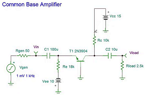
Take the following example of a Common Base arrangement from a
Professor.
The circuit is correct, and the instructor gets the same values, but I
use simple voltage-division understanding. Where are you going to get minus 0.7v for
the emitter?
Secondly, it is much better to let the transistor generate its own set
of conditions, (as we have done in the circuit above), rather than force
it into some unknown state ( I call it an "overloaded state") by feeding the emitter with current from a
10v supply. This puts 0.5mA current through the transistor when in
resting mode. This high current is going to swamp any change and is not
a good way to load a circuit.
1mV signal with 50 ohm impedance will deliver a current of 0.02mA
The collector current will be altered by 0.02mA and this will produce a
voltage swing of 0.02 x 2,000 = 40mV (as the load is actually a
10k resistor and a 2k5 resistor - making 2k load).
I have shown how to solve this circuit with the minimum of mathematics, and you will be able
to do it too, when you realise what is each component is doing and how
the circuit works.
All circuits have to be drawn as shown above so you can see the
positioning of the leads of the transistor, and not how the the
transistor is drawn below. By drawing the transistor correctly you will
be able to see how the voltages are developed and delivered to the
transistor.
You have to do all this in your head so you can work on a circuit and
design it and fix it.
MORE TECHNICAL
I didn't want to get more
technical, but Instructors on YouTube are making such absurd claims
about the circuit that I have to respond.
The output of the circuit (on the collector) has the same current
capability of the device delivering the signal to the circuit.
The transistor provides no current amplification.
In most cases the input device will produce a very small voltage, have a
very small current-capability and have a very low impedance
(resistance). After all, that's the purpose of this circuit.
Since the output current from the collector will be very small, the
output impedance is said to be VERY HIGH. A Very High output impedance
has very little current capability and we do not talk about its voltage
capability. The voltage capability depends on the characteristic
of the transistor.
When we have a High Impedance output, we must connect it to a High
Impedance load.
Let's say the output is 1M. (we will explain how to arrive at this value
later).
If you connect the output to 1M load, the amplitude will drop to 50%.
If it is 10M the output will drop to 90%. You can work out the
in-between values yourself.
HOW DO YOU WORK OUT THE OUTPUT IMPEDANCE?.
If you have a 12v supply and load is 10k, you will need a current of
1.2mA to produce 12v across the resistor.
But you only have 0.5mA available from the collector.
A load of 24k will produce a voltage of 12v across the load when 0.5mA
flows.
Most Common Base circuits have a current capability of 0.1mA and you
will need a 120k load to produce 12v when 0.1mA flows.
This is a HIGH IMPEDANCE output. If the output load is 120k, the
signal will be reduced to 50%.
That's why the circuit above has a bootstrap circuit to take the output
of the common base circuit and deliver it to an output, without loading
the common base arrangement.
The bootstrap circuit is not a load. It is a "detector." It is
detecting the output voltage and "rises" according to the increase in
voltage and delivers this increase to the output with about 100 times
more current than the common base circuit can deliver.
Any other load will severely reduce the output.
Page-1 Common-Emitter stage Go to
Talking Electronics
website
13/9/2023
Page1A. more on the stages
Page-2 emitter-follower - common collector stage
Page-2A common base stage
Page 3 Coupling stages
Page 4 More on Coupling Stages
Page-5 The FLIP FLOP
The REAL
Transistor Amplifier