Here is a toggle circuit that does not work. Pin 2 detects less than 33% of
rail voltage and pin 6 detects more than 66% of rail voltage.
These two pins are being held at 50% of rail voltage via the two10k
resistors. The problem is this: The 100k resistor from the output of the
chip will not raise or lower the two pins by the 15% needed to change the
state of the circuit. If the two 10k's are changed for 100k and the 100k
changed for 10k, the circuit will work.
However we have a time-delay created by the 1u and if the switch is pressed
for too-long, the circuit will change back to it original state.
An improved design places the switch as shown below: The 1u is now charged
to about rail voltage or about 0v via the action of the output of the chip
and this voltage is immediately delivered to pins 2&6 via the switch. If the
switch is kept pressed, the ratio of the resistors will not cause the chip
to change states, as discussed above.
Simply changing the position of the switch turned a faulty circuit into a
success.
One further problem with the 555 is this: Pin 3 does not go below about 0.6v
and the 2N3904 transistor does not fully turn off.
Fit a 2k2 between the base and 0v to reduce the voltage on the base to fix
this problem.
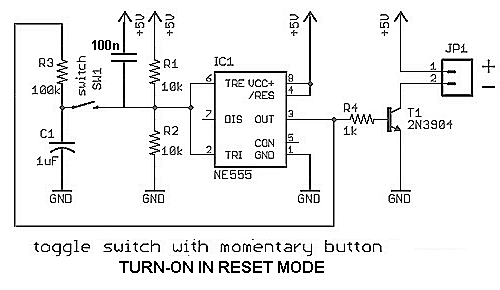
Some readers have asked for the circuit to turn-on in RESET mode.
Pin2 detects a LOW to make the output HIGH. If a 100n capacitor is placed
across the upper 10k, the 555 will turn on in RESET mode.
Here's an example of "clear thinking."
In other words, look at the problem and see if it can be solved very simply.
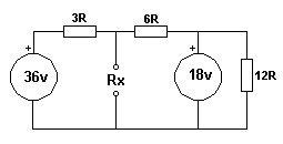
Here is the answer from a reader with "mathematical understanding."
Using the node method, find the voltage across Rx in terms of Rx.
Use E^2/Rx and find the term for power across Rx in terms of Rx
Find the first derivative of the power with respect to Rx and solve for its
zero value.
When Rx = 18 ohms, the maximum power is obtained.
The above reasoning is entirely WRONG.
The circuit is very complex until you realise one thing.
Firstly, remove the 6R, 18v and 12R.
Maximum power in Rx is achieved when Rx is equal to 3R.
To see if this is true, simply change Rx to 2R or 4R and work out the watts
dissipated.
Another way to look at it is this: When Rx is zero, the watts dissipated is
zero, when Rx is very high, the watts dissipated is very small.
Make Rx = 3R and see what happens:
The voltage across Rx will be 18v.
Now put-back the 6R, 18v supply and 12R load resistor.
The voltage across Rx is 18v. This means no current will flow though the 6R
resistor because it has 18v on each end.
Current through Rx = 36v/6R = 6 amp
Wattage dissipated by 3R = V2/3 = 108watts or
2xR = 62
x 3 = 108watts
We have turned a seemingly complex question into a very simple answer.
Here's another disastrous
circuit from
D.Mohan Kumar:
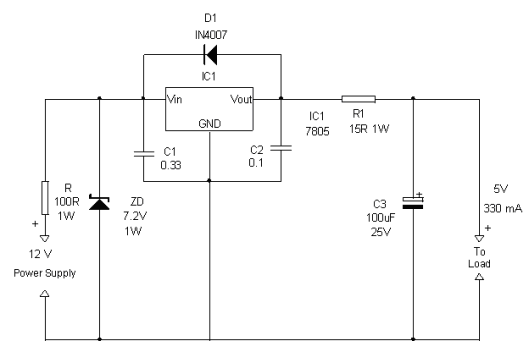
The 100R resistor on the input has 12v - 7.2v = 4.8v across it and 48mA will
flow through the resistor and 7.2v zener.
Suppose the power supply delivers 20mA to a load. The 7805 takes 10mA,
making a total of 48+20+10 = 78mA
The voltage across the 100R will increase to: V = 0.078 x 100 = 7.8v
The input voltage will be: 12v - 7.8v = 4.2v The power
supply cannot even deliver 20mA!!!!!!!!
This is another of Professor D.Mohan Kumar's
disasters. He should stop putting rubbish like this on the web. He doesn't
know a thing about electronics.
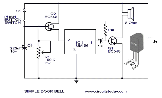
Here's a circuit from D.Mohan Kumar
and other Indian websites, that does not work. They copy each other and
never build the circuit. They obviously think "it'll work" because I am a
Professor!
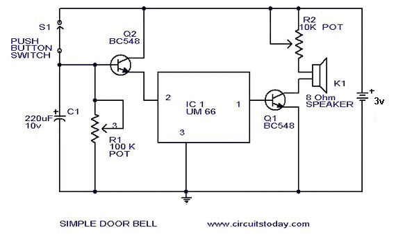
The output of the UM66 is not sufficient to turn on the transistor. It may
work for some transistors and it may work when the load is very high. But it
doesn't work for the circuit above.
The solution is to self-bias the output transistor and couple it to the chip
with a capacitor.
Always build EVERY circuit
before putting it on the web. You never know what fault will come out of
even the simplest circuit.
The UM66 series of chips have a range of tunes. The UM66T19L outputs "For
Elise." The other chips are listed below. When ordering, make sure you ask
for the exact song you require.
Here is the list of different chips and their content:

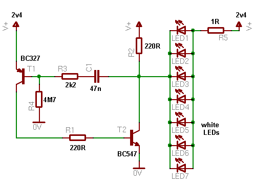
Here's a simple circuit driving 16 white LEDs from the mains.
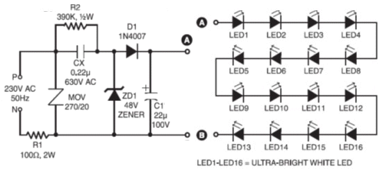
Here's three technical mistakes from a chief electronics editor:
1. He says:
"The 48V zener is there to clamp the supply to the LED chain to +48V
maximum."
Not true.
If it actually did that, the LEDs would not work or be very dull. The REAL
purpose of the zener is to discharge the capacitor.
2. He says:
The current through the LEDs is 25mA.
Not true. The current though the LEDs is about 7mA
3. He says:
"With the 22uF present during the negative half cycle,
the 22uF supplies a lower holding current to the LED's so they do not go
completely off."
See discussion below.
He also falsely thought the LEDs would
flicker at 25Hz on a 50Hz supply.
The current is limited by the 0.22u capacitor and it is a capacitor-fed
power supply that is commonly known as a CONSTANT CURRENT SUPPLY. In this
case the current is limited to 7mA.
At 7mA the voltage across a white LED is 3.3v. At 3mA the voltage is 3v.
Without the electrolytic, the LEDs produce a noticeable flicker.
This is because they are being fed pulses during the positive half-cycle and
turn-off completely during the negative part of the cycle.
The voltage only has to drop from 16 x 3.3 = 53v to 16 x 3 = 48v and the LEDs do not
illuminate.
This means they are only illuminating during the top 10% of the voltage-curve and
when this is analysed on a width-basis, it represents about 50% ON-time.
You can observe this by setting up the circuit and shaking it from
side-to-side and see when the LEDs are illuminated.
When the electrolytic is added, some of the current charges it during the
peak of the waveform and as the waveform reduces, it delivers this energy to
the LEDs to keep them illuminated during the dip in voltage.
The electrolytic would be much more effective if it were connected to the
supply voltage with a 470R connected to the LEDs. This would allow it to be
charged to a higher voltage so it can deliver its energy during the
remainder of the cycle.
In fact the circuit will not work with 16 LEDs as they drop 16 x 3.3v = 53v.
The zener limits the voltage to 48v and the LEDs will be very dull.
The zener should be replaced with a 1N4004 diode.
It's a very poorly designed circuit with at least 3 faults.
See: "30 LED Circuits" eBook for a number of correctly-designed
circuits.
This circuit produces a constant 350mA to illuminate a 1 watt LED. The
circuit is over-designed.

The circuit can be reduced to 2 components:
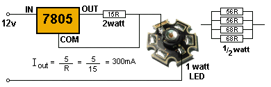
The 7805 can be converted into a content-current device by connecting a
resistor as shown above.
We will take the operation of the circuit in slow-motion to see how it
works.
As the 12v rises from 0v, the 7805 starts to work and when the input voltage
is 4v, the output is 1v as a minimum of 3v is lost across the 7805. The
voltage rises further and when the output is 5v, current flows through the
15R resistor and illuminates the LED. The LED starts to illuminate at 3.4v
and the voltage across the 15R at the moment is 1.6v and the output current
will be 100mA. The input voltage keeps rising and now the output voltage is
7v. The current through the LED increases and now the voltage across the LED
is 3.5v. The voltage across the 15R is 3.5v and the current is 230mA.
The input voltage keeps rising and the output voltage is now 8.6v The
current through the LED increases and the voltage across the LED is now
3.6v. The voltage across the 15R is 5v and the current is 330mA. The input
voltage keeps rising but a detector inside the 7805 detects the output
voltage is exactly 5v above the common and the output voltage does not rise
any more. The input voltage can rise above 13v, 14v . . . . 25v or
more but the output voltage will not rise.
If the output voltage rises, more current will be delivered to the LED and
the voltage across the 15R will increase. The 7805 will not allow this to
happen.
The LED will have 3.6v across it. The 15R will have 5v across it and the
output will be 8.6v. The input voltage will have to be at least 12.6v for
the 7805 to operate.
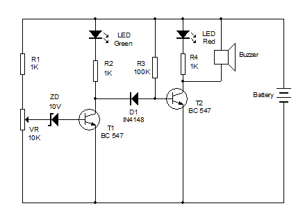
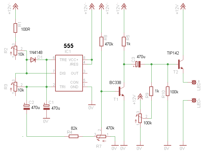
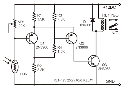
Here's another over-designed circuit by Professor D.Mohan Kumar.
The 555 is consuming 10mA all the time and this is very wasteful when using
a 12v battery.
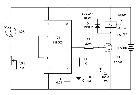
The transistor circuit consumes less than 0.1mA when the relay is not
activated. It is also simpler and cheaper to construct.
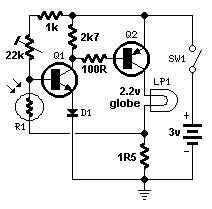
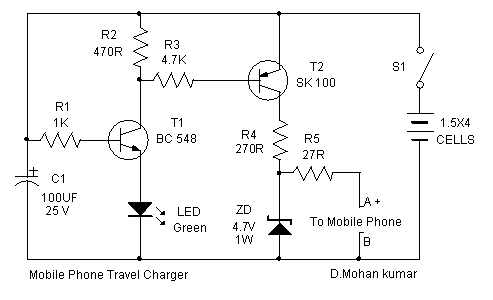
Another over-designed circuit by Professor D.Mohan Kumar.
SOLAR NIGHT LIGHT
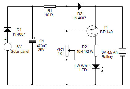
1. What is the purpose of D1? It is not needed.
2. What is the purpose of C1? It is not needed.
3. If the LED is 1w and has about half rail voltage across it, R2 will also
have half rail-voltage across it and it needs to be 1 watt also.
4. Turn VR1 to zero ohms and it will burn out via the emitter-base junction
of T1.
5. A 4.5Ah battery needs to be charged at about 400mA. 400mA flowing
through R1 will produce a voltage drop of 4v. The 6v solar panel
will never charge the 6v battery.
This is just a junk circuit that will never work.
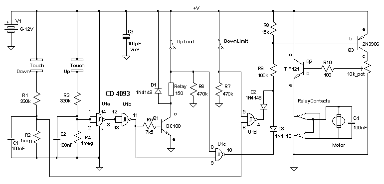
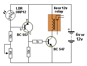
Here's an interesting circuit. Let's look at the design.
The first two transistors are connected to form a PNP Schmitt Trigger.
This give a fast action to the relay. But this is not needed. The action of
the relay turns ON and OFF in the second circuit without any problem and it
does not need a diode across the relay because the transistor is turning OFF
slowly.
Firstly, you don't need 3 transistors to operate a relay from an LDR (Light
Dependent Resistor).
When light falls on the LDR, the relay turns OFF.
Here is a circuit that turns OFF a relay when light fall on the LDR and
requires only 2 transistors:
Let's look at the first transistor in the 3-transistor circuit:
When no light falls on the LDR, the transistor is OFF.
The voltage divider made up of the 7k5, 1k5 and 2k2 puts 4v on the
base of the second transistor. This turns ON the second transistor and the
emitter will be about 4.6v. This will turn ON the third transistor and also
the relay.
As light falls on the sensor, it forms a voltage-divider with the 22k.
The emitter of the first transistor is 4.6v and when the base is 4v due to
the resistance of the LDR, the first transistor starts to turn ON. This
increases the voltage across the 2k2 resistor and has the effect of turning
OFF the second transistor. The voltage across the 1k5 reduces and turns ON
the first transistor slightly more. After a short period of time the first
transistor is turned ON FULLY and the second transistor is fully tuned OFF.
This action occurs without the LDR changing resistance. This is the action
of the Schmitt Trigger.
The circuit does work but is over-complex for the requirement.
Here's a circuit from Electronics Maker, an Indian magazine. It looks
fairly workable at first glance, but let's look into it in more
detail:
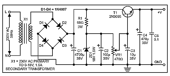
The transformer is not referred to as "Secondary: 0-18v." It is simply
240v:18v. An 18v secondary will normally be 5v higher than the rating to
account for voltage-drop under load. This means the output will be 23v and
when this is rectified, it will produce a voltage of 23 x 1.4 -2v = 30v.
The 68ohm resistor will drop 30v - 18v = 12v. The current though the 68R =
175mA.
This current will also flow through the 18v zener. The wattage
dissipated by the zener will be:
18v x 0.175 = 3.15 watts. The circuit specifies 1.5watt. The
zener will be damaged !!
The 2N3055 has a gain of about 50.
Suppose you turn the pot to produce 9v. It will be at approx
235ohms.
When the transistor is delivering 1A, the base current will be 1,000/50 =
20mA. This current will flow through the 235 ohms of the pot and the voltage
drop will be: .02 x 235 = 4.7v.
The output voltage will DROP 4.7v !!
This is a typical JUNK CIRCUIT. It has not been tested and no-one from the
magazine has picked up the mistakes.
For a 1Amp Power Supply, it would be much better (and cheaper) to use a
3-terminal regulator such as LM317. It is adjustable from 1.2v. It has
almost no drop in output voltage and the ripple is about 5mV.
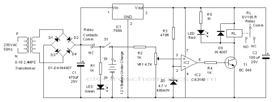
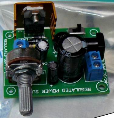
Here is a kit using the LM 317 regulator. You can see the two different inputs
(power plug and flying leads), WO4 bridge rectifier and pot to adjust the
output voltage. The regulator will need a larger heat-fin if you want to deliver
more than 200mA.
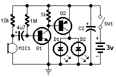
Here's a circuit from someone who knows nothing about designing. It has a
number of mistakes.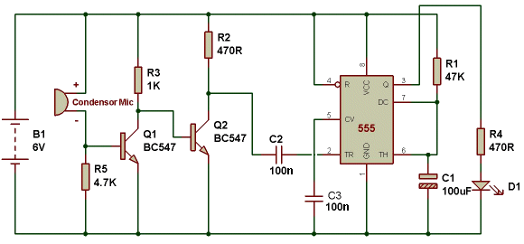
The condenser microphone is actually called an electret microphone and it
will be totally damaged in the circuit above.
It is connected directly across the supply with a base-emitter junction of
the fist transistor. It needs a 10k resistor in series with the microphone.
It is not a good idea to connect the microphone directly to the input of the
transistor, however it can be done. The transistor must be only lightly
turned-on so the signal can be amplified.
This is very hard to judge and if a series resistor is adjusted from
10k to 1M, you will see the change in output signal.
This is a huge range and will depend on the type of microphone. That's why
you cannot present a circuit with such a wide range of values.
The 4k7 resistor is not doing anything and can be removed.
The 1k and 470R resistors are too low. They should be 22k to 47k.
Pin 2 of the 555 is not being held HIGH via a 100k so it can be taken LOW
via the signal from the second transistor.
The whole circuit is a bad design. It is taking 10mA when sitting around and
does not offer an ON-OFF feature but simply a delay when a clap is detected.
The circuit should be avoided.
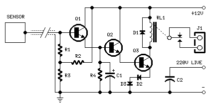
Here is a 2-transistor Switch-Mode Power Supply from
Roman Black. He
has shown the operation of the circuit using 4 diagrams but they do not
actually explain HOW THE CIRCUIT WORKS. In fact the diagrams are hard
to decipher and misleading. He is a correct description of the operation of
the circuit.
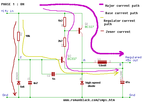
The circuit shows 2 transistors, an inductor L1 and high-speed diode D1.
Here's how the circuit works:
PHASE 1: ON
The circuit does not turn on until the output is slightly less than 5v.
The voltage on the base of Q2 is 5v6 and the emitter is slightly less
than 5v. This produces a slightly higher base-emitter voltage and causes Q2
to turn ON. This turns on Q1 via the 2k7 resistor.
Current flows through inductor L1 and it builds up a magnetic flux. This
magnetic flux produces a voltage across the inductor that is almost equal to
the difference between the 5v output and the supply. This allows Q1 to turn
on. The inductor can keep producing this "back voltage" until the the core
becomes saturated. At this point the back voltage suddenly ceases and the
right plate of the 1n drops a small amount. This is transferred to the base
of Q2 to turn it off slightly.
This action continues between the two transistors until they are both fully
turned off.
The large purple arrow is correct.
The thin purple arrow is vague and the description of the yellow arrow is a
mystery.
PHASE 2: TURN OFF
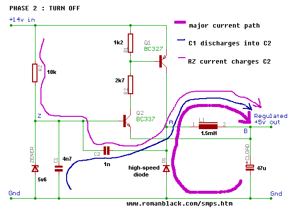
The arrows above are vague and misleading and incorrect. See Phase 2A below
for correct description.
PHASE 2A: TURN OFF
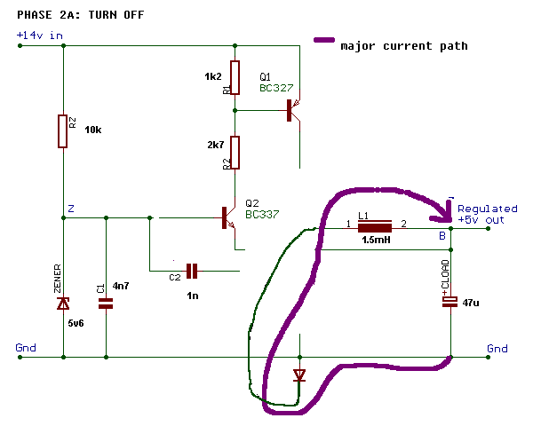
When the two transistors turn off, the magnetic flux in the inductor
collapses and produces a voltage IN THE REVERSE DIRECTION to the applied
voltage. This means the left side of the inductor produces a voltage that is
LESS THAN 5v. This pulls the voltage on the base of Q2 lower and turns
off the transistor even MORE. At the same time it charges the 1n and C1 is
discharged slightly.
If the voltage on the left side of L1 reaches -0.6v, the high-speed diode
"flips-over" and starts to conduct. This stops the left side of the inductor
creating a higher negative voltage and now any energy produced by the
inductor is passed to the 5v regulated output. This is how the energy from
the inductor adds to the output.
PHASE 3: OFF (Delay Period)
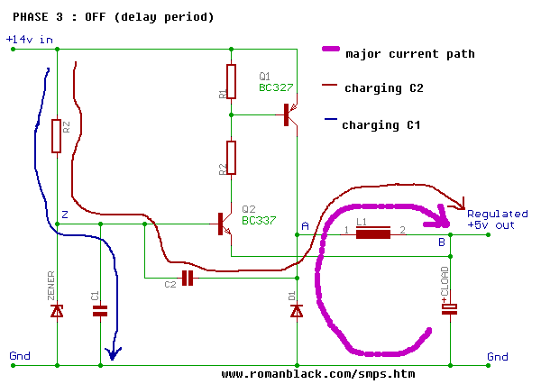
I don't know what is trying to be explained in Phase 3. I don't know what
the author means by "Delay Period" He thinks the delay period is
set by C1, C2. This is not so. The releasing of the energy from the inductor
sets the time for this part of the cycle.
Both C1 and C2 are charged by a very small amount by Rz.
PHASE 4: TURN ON
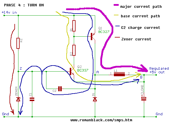
The energy in the inductor is very soon passed to the output and the voltage
across L1 reduces. The voltage on the right-hand side plate of C2 rises from
-0.6v and the energy in C2 charges C1 and turns on Q2.
The yellow base-current path does not pass through R1 but the emitter-base
junction of Q1 passes about 1mA and R1 passes about 0.5mA.
As you can see, arrows on a diagram are misleading and meaningless. The
author did not have an understanding of the operation of the circuit and
this confused me greatly.
I could not follow the operation. That's the purpose of a language. It
explains things clearly and accurately.
I did not receive a reply until a reader posted this discussion on an
electronics website.
Roman replied on the website:
"I had just chosen to ignore it, believing my description was fairly
accurate and easy to understand."
Things cannot be "fairly accurate" They are either accurate or not.
Roman replied to some of my comments and got himself further entwined in
inaccuracies. That reinforced my comment that he did not know how the
circuit worked.
He said: "The turning off phase involves the discharge of caps. As the buck
turns off, the inductor pin point A slams below 0v, this causes C1 to
discharge and the +ve voltage in C1 to cause a current through C2, as shown
by my blue arrow."
The "turn off" phase is a transitory phase where C1 energy is dumped through
C2 causing the voltage on point Z to drop sharply as C1 energy is dumped
through to the load.
This is entirely untrue.
The timing of the "Off Period" is controlled by the energy in the inductor.
Refer to Phase 2A where I have shown the high-speed diode sits below the 0v
rail and will have -0.6v on the cathode.
The right lead of the 1n will drop from about 12v (in one direction) to -0.6v
(in the other direction) and this 13v is called "energy" and it will
discharge the 4n7 by an amount equal to the ratio of the two capacitors.
That's why the 4n7 drops about 3v. The voltage on C1 will go below the zener
voltage and the 10k will provide a small current to "top up" C1 and
C2. This means that the energy in the two capacitors will be slightly more
than at the beginning of this part of the cycle and when the energy from the
inductor has been fully released, the voltage on the cathode of the high
speed diode will start to rise due to the voltage on the electrolytic on the
output and the resistance of the inductor. As the voltage rises, the energy
in C2 will be passed to C1 and the voltage on the base will rise to 5v6. The
energy will do two things. It will pass into the zener diode and also into
the base of Q2 to turn it ON.
This turns on Q1. This raises C2 to turn on Q2 further. The small
amount of energy provided by the 10k Rz resistor provides the energy into
the base of Q2 to start the next cycle.
Roman further states:
It is common in SMPS buck ICs to use a "timed off" period, usually a
monostable. I managed to mimic this effect by the combination of C1 and C2
and the energy dump as explained in Phase2. Once C1 has dumped and is at 3v,
there is a clearly defined "delay period" while C1 charges again (via RZ)
and during this delay period the buck Q1 remains off. This gives a big drop
in frequency and improves efficiency for a number of reasons, and also
greatly increases stability.
Roman is mixing up the defined "timed off" period in a buck IC circuit with
the 2-transistor circuit above. The capacitors C1 and C2 have no effect on
the frequency. The frequency is generated by the time it takes to release
the energy from the inductor during the "turn off" period.
He says: "The "turn off" phase is a transitory phase where C1 energy is
dumped through C2 causing the voltage on point Z to drop sharply as C1
energy is dumped through to the load." This is incorrect. The energy is not
passed to the load as the right hand end of C1 is connected to the cathode
of the high-speed diode and it is CONDUCTING during this part of the cycle
and the energy from C1 is being LOST.
This is a clear factor that he does not understand the operation of the
circuit.
I have been criticised for stating this FACT, but how else can you describe
an article that is COMPLETELY WRONG!
He believed his descriptions were "fairly accurate."
You be the judge.
1. He never once mentions the fact that the inductor produces a reverse
voltage. This is the crux to the operation of the circuit.
2. He never shows the high speed diode "flipping over" and conducting.
3. He concentrates on current through the 10k entering the load. This is
less than 1mA.
4. He thinks the frequency of the circuit is generated by C1 and or C2.
This is not so.
5. He says energy from C2 is dumped into the load. This is not so. It is
LOST.
6. He says the charging of C2 is via Q1, but initially it is via the
electrolytic (at the load).
In simple terms, the operation of the circuit is this:
The high voltage from the supply is passed to the load via the inductor.
The two transistors turn on very quickly and the current flows to charge the
electrolytic on the output. This current passes through the inductor and
produces magnetic flux.
This magnetic flux produces a "back voltage" that allows Q1 to turn on
fully. At a point in time the core of the inductor becomes saturated and the
"back voltage" ceases. At this point the voltage on the collector
reduces and this is passed to the base of Q2 via the 1n capacitor.
The two transistors turn each other OFF and the magnetic flux collapses and
produces a voltage in the opposite direction.
The rest of the cycle has
been covered above.
Page 11
Page 2
Page 3
Page 4
Page 5
Page 6
Page 7
Page 8
Page 9
Page 10
Page 11
Page 12
Page 14