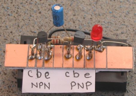
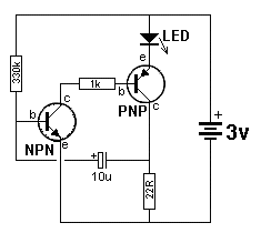
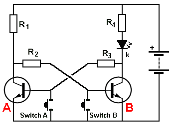
The transistor tester allows you to test a
transistor and find out if it is NPN or PNP and identifies the leads.
Simply connect both transistors to the circuit and the LED will flash.
Replace one of the transistors with an unknown transistor and try all
the leads around every different way. If the circuit does not
work. Try the other 3 pins.
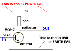
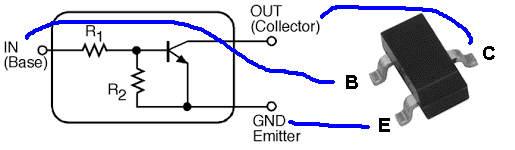
BASE VOLTAGE
You cannot "put" or "connect" a voltage higher
than 0.7v on (or to) the base of a transistor - that is: between the
base and emitter leads. The structure inside a transistor - between the
base and the emitter - is effectively similar to a diode and if you
apply a voltage greater than 0.7v, the transistor will BLOW UP!
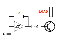
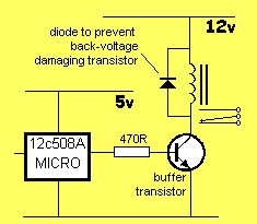
To prevent this, we place a resistor on the base and the resistor drops
the required voltage so the transistor is not damaged. That's why you
will see a base resistor (a resistor in the base - on the base)
in the circuits below.
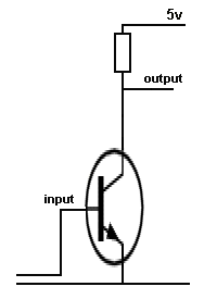
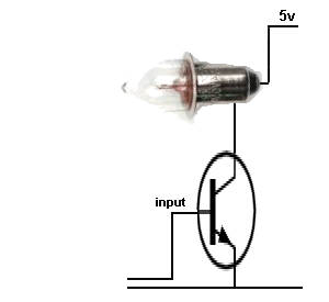
THE DIGITAL TRANSISTOR
There is no such thing as a DIGITAL TRANSISTOR or ANALOGUE
TRANSISTOR. Transistors are either called "SMALL SIGNAL"
or "POWER." However there is a
surface-mount transistor with 3 leads, called a DIGITAL TRANSISTOR. It
is an ordinary transistor with 2 resistors included inside the "package"
so it can be connected directly to a digital circuit. (so the base lead
can receive 0v to 5v and not damage the transistor) Resistor R1 allows a
voltage of 5v to be connected to the pin called "B." This pin is not the
base of the transistor but an INPUT pin.
The
digital transistor has two resistors included inside the case
R1 is about 10k and R2 is approx 47k
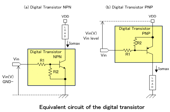
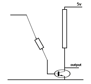
These transistors
can be made to work in analogue circuits
because they are ordinary transistors with a 10k base resistor,
but you will have to know what you are doing.
It is the components in the circuit and the signal entering the
circuit that create a DIGITAL STAGE or ANALOGUE STAGE. The transistor
can also operate at high frequency or only at low frequencies and it can
be a high voltage circuit or only a low voltage circuit.
When we say "Digital Transistor" we mean the circuit is a digital
circuit or digital stage and the input signal changes from one state to
another VERY QUICKLY. A slow rising and falling signal
creates an analogue stage.
A digital transistor will work in an analogue circuit as an ANALOGUE
TRANSISTOR ! |